Five Key Steps to High-Speed NAND Flash Performance and Reliability
|
|
|
- Elfrieda Thomas
- 6 years ago
- Views:
Transcription
1 Five Key Steps to High-Speed Flash Performance and Reliability Presenter Bob Pierce Flash Memory Summit 2010 Santa Clara, CA 1


2 NVM Performance Trend ONFi 2 PCM Toggle ONFi 2 DDR SLC Toggle Performance DDR MLC Async MLC Corrected MMC Async SLC Device Cost
3 Five Steps to obtaining Reliability and Performance 1. Utilizing Device commands and parameters 2. Architecture advancements 3. Error correction improvements 4. Maximizing Interface performance 5. Using Software and hardware to maximize objectives Flash Memory Summit 2010 Santa Clara, CA 3
4 Keys to Flash Device Performance Page Size increases 2,4,8 K page size What is the impact to bit growth and addressing? Read, Write Cycles have been pretty stable From 30 to 6 nsec range Key Timing Parameters Trc, Twc, Tprog, Tr, Tbers Flash Memory Summit 2010 Santa Clara, CA 4


5 Critical Timing of Flash In nsec Flash Memory Summit 2010 Santa Clara, CA 5
6 Command and Architecture Improvements Multi Plane Bus turn-around time Ability to transfer data Multi device switch performance LUN Addressing Multiple Access capability LUN addressing Volume Support Cache Read Cache write Pipeline read Pipeline write Enhanced commands Higher Bus Speed (Toggle, ONFi 2)
7 System Performance Benefits Enhanced commands Small Data Move command if supported, allows the host to transfer data to the page register in increments that are less than the page size of the device for both Program and Copy back operations. Bandwidth Ability to utilize the larger page sizes Reducing read and write page access cycles Command pipe lining Improving read modified write operation
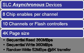
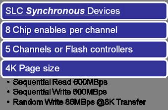
 2K page: 42µs 4K page: 86µs Microseconds For legacy reads, performance is artificially limited to 40 MB/s Today for SLC the I/O time is")

8 Challenges: Latency Increases as Lithography Shrinks component performance is determined by two elements: array access time Data transfer across the bus I/O time for Page (trc=20ns) 2K page: 42µs 4K page: 86µs Microseconds For legacy reads, performance is artificially limited to 40 MB/s Today for SLC the I/O time is 2-4x the array transfer time As page sizes increase, latency becomes large Especially for small reads array read transfer time SLC: tr time is normally 20-25µs MAX MLC: tr time is normally 50µs MAX I/O performance must be less than or equal to array performance for maximum sustained read throughput Data supplied by Micron


9 System Performance
10 Sequential vs. Random Operations Sequential operation typical applications Card Based solutions USB, MMC etc Storage of data, pictures, videos, boot image Random Operations Embedded Systems SSD s Caching Storage of data, active memory access and storage. Flash Memory Summit 2010 Santa Clara, CA 10

 are typically high latency")
11 ECC Trend Typical use more than one type of Error Correction i.e. 8 and 30bits DSP and LDPC (Low Density Parity Check Code) are typically high latency Solutions BCH (Bose and Ray-Chaudhuri) should be close if not at Line rate. Flash Memory Summit 2010 Santa Clara, CA 11
12 Error Correction Code Comparison BCH Long BCH LDPC Latency Low Medium High Decoder Throughput Very High High Medium Gate Counts Small Medium Large Overhead Size Very Small Small Small Error Correction Capability Limited Better Best
13 Cadence Nand w PHY Support Command and data Interrupt AHB/AXI Cmd/ Data Interface Map 00 Buff Access Map 01 Array Access Sequencer/ Status Module Async Buffer Map 10 Control Access Data AHB/AXI Initiator Interface Map 11 Direct Access ECC Register Information AHB/AXI Port Register Interface Internal Registers Interrupt
14 Centralized LDPC Hardware Architecture BUFFER HOST SYSTEM P H Y Host Interface DMA RAM Multi-Port Arbitration Unit CMD & DATA DMA CMD & DATA DMA Channel 1 Channel 2 ECC, CRC Other ECC, CRC Other P H Y P H Y 1 x Devices 1 x Devices 1 x controller channels LDPC Processor CMD & DATA DMA Channel n ECC, CRC Other P H Y 1 x Devices
15 Centralized ECC Hardware Architecture BUFFER HOST SYSTEM P H Y Host Interface DMA RAM Multi-Port Arbitration Unit Channel 1 Channel 2 CRC CRC P H Y P H Y 1 x Devices 1 x Devices CMD & DATA DMA 1 x controller channels LDPC BCH, ECC Processor Channel n CRC P H Y 1 x Devices Buffer
16 Key Aspects to System Performance Improvements Increase the number of commands to the flash device Maximizes the number of transactions that a device can do Toggle is capable of 125% more Read bandwidth over typical asynchronous devices Fast error correction and identification of errors Improves block management throughput Reduces processor overhead Reduce Interrupts to processor Improves the number of transactions, address translation Improves ECC performance Improves background process operation Removes software timer requirements
17 Performance System Architecture Applications DRAM SSD UFS Cache Enterprise Host High Speed ECC Central LDPC 32 Bit Processor WL, Blk. Policy ONFi 2 / Toggle ONFi 2 / Toggle ONFi 2 / Toggle ONFi 2 / Toggle ONFi 2 / Toggle Highest Performance Most flexibility for Block Policy Architectural Flexibility Highest Error Correction Solution Command Q to maximize Bus utilization SSD HS USB 3.0 Cache Module DRAM Host Block Management Wear Leveling 32 But Processor SRAM ECC, DSP Corrected Reduced HOST Resources Known good Data Higher data latency Easier to keep up with shrink Path Less flexible for block policy Card based USB 2/3 MMC Host 16 bit Wear Leveling Min. Block Mgr. SRAM High Latency Poor Random performance Block management slow Hard to keep up with HS Flash Basic ECC operation Low write count
18 Five Trends to watch 1. Nand Device architectures and commands have to continue to improve. Array performance is degrading, command and architecture improvements must continue. 2. ECC Solutions are more complex and have become the corner stone to improved data reliability and Block Policy management. 3. New controller architectures must continue to evolve based on system requirements and complex architectures. (One size not fit all) 4. Interface data rates have to increase to maximize multi chip transfer rates and increase through put. (higher transfer rate) 5. Software complexity utilizing new error correction methods are more complex, management is comprised of multiple solutions all requiring some decision properties. Flash Memory Summit 2010 Santa Clara, CA 18
High-Speed NAND Flash
 High-Speed NAND Flash Design Considerations to Maximize Performance Presented by: Robert Pierce Sr. Director, NAND Flash Denali Software, Inc. History of NAND Bandwidth Trend MB/s 20 60 80 100 200 The
NAND Flash Architecture and Specification Trends
 NAND Flash Architecture and Specification Trends Michael Abraham (mabraham@micron.com) NAND Solutions Group Architect Micron Technology, Inc. August 2011 1 Topics NAND Flash trends SSD/Enterprise application
Error Control Coding for MLC Flash Memories
 Error Control Coding for MLC Flash Memories Ying Y. Tai, Ph.D. Cadence Design Systems, Inc. ytai@cadence.com August 19, 2010 Santa Clara, CA 1 Outline The Challenges on Error Control Coding (ECC) for MLC
Optimize your system designs using Flash memory
 Optimize your system designs using Flash memory Howard Cheng Sr. Segment Applications Manager Embedded Solutions Group, Micron 2012 Micron Technology, Inc. All rights reserved. Products are warranted only
The Evolving NAND Flash Business Model for SSD. Steffen Hellmold VP BD, SandForce
 The Evolving NAND Flash Business Model for SSD Steffen Hellmold VP BD, SandForce Solid State Storage - Vision Solid State Storage in future Enterprise Compute Anything performance sensitive goes solid
Flash Controller Solutions in Programmable Technology
 Flash Controller Solutions in Programmable Technology David McIntyre Senior Business Unit Manager Computer and Storage Business Unit Altera Corp. dmcintyr@altera.com Flash Memory Summit 2012 Santa Clara,
Transitioning from e-mmc to UFS: Controller Design. Kevin Liu ASolid Technology Co., Ltd.
 Transitioning from e-mmc to UFS: Controller Design Kevin Liu ASolid Technology Co., Ltd. Flash Storage Summits 2 Agenda emmc vs. UFS Flash Trend & Challenges Key Requirements for Embedded Controller Design
The Many Flavors of NAND and More to Come
 The Many Flavors of NAND and More to Come Brian Shirley VP Micron Memory Product Group 1 NAND Market Growth Drivers Top 10 Applications by Units Shipped 4000 # of Units per Application 3500 Millions of
How Good Is Your Memory? An Architect s Look Inside SSDs
 How Good Is Your Memory? An Architect s Look Inside SSDs Michael Abraham (mabraham@micron.com) Business Line Manager Micron Technology, Inc. August 2015 1 Early Storage Optimizations µc NAND Camera SmartMedia
Virtual Storage Tier and Beyond
 Virtual Storage Tier and Beyond Manish Agarwal Sr. Product Manager, NetApp Santa Clara, CA 1 Agenda Trends Other Storage Trends and Flash 5 Min Rule Issues for Flash Dedupe and Flash Caching Architectural
An LDPC-Enabled Flash Controller in 40 nm CMOS
 An LDPC-Enabled Flash Controller in 40 nm CMOS Marvell Semiconductor Engling Yeo Santa Clara, CA 1 Outline Error correction requirements LDPC Codes ECC architecture SOC integration Conclusion Santa Clara,
NAND Flash Memory. Jinkyu Jeong Computer Systems Laboratory Sungkyunkwan University
 NAND Flash Memory Jinkyu Jeong (Jinkyu@skku.edu) Computer Systems Laboratory Sungkyunkwan University http://csl.skku.edu ICE3028: Embedded Systems Design, Fall 2018, Jinkyu Jeong (jinkyu@skku.edu) Flash
3D NAND - Data Recovery and Erasure Verification
 3D NAND - Data Recovery and Erasure Verification Robin England Hardware Research & Development Team Lead Santa Clara, CA The Causes of SSD Data Loss What can go wrong? Logical Damage Data accidentally
Memory Device Evolution
 Memory Device Evolution Cassino May 2008 Maurizio Di Zenzo Applications Lab Mgr Agenda Random access memories A quick comparison of technologies Details of external memory technologies Solutions for low
Flash Memory Overview: Technology & Market Trends. Allen Yu Phison Electronics Corp.
 Flash Memory Overview: Technology & Market Trends Allen Yu Phison Electronics Corp. 25,000 20,000 15,000 The NAND Market 40% CAGR 10,000 5,000 ($Million) - 2001 2002 2003 2004 2005 2006 2007 2008 2009
Making Informed Memory Choices FTF-IND-F0378
 Making Informed Memory Choices FTF-IND-F0378 Freescale Technology Forum Jim Cooke JCooke@micron.com Mike Kim MikeKim@micron.com April 10, 2014 2014 Micron Technology, Inc. All rights reserved. Products
Hardware NVMe implementation on cache and storage systems
 Hardware NVMe implementation on cache and storage systems Jerome Gaysse, IP-Maker Santa Clara, CA 1 Agenda Hardware architecture NVMe for storage NVMe for cache/application accelerator NVMe for new NVM
Optimizing Your Memory Sub-System
 Optimizing Your Memory Sub-System AKA Choosing the right memories Design with Freescale Toronto Jim Cooke Ecosystems Enablement JCooke@micron.com Les Marentette FAE Manager LMarentette@tech-trek.com November
Improving NAND Throughput with Two-Plane and Cache Operations
 Improving NAND Throughput with Two-Plane and Cache Operations Introduction SLC NAND Flash memory is quickly being integrated into embedded systems for data and code storage. This technical note introduces
Can Embedded Applications Utilize the Latest Flash Storage Technologies?
 Can Embedded Applications Utilize the Latest Flash Storage Technologies? Grady Lambert Sr. Director, Embedded Engineering Swissbit Santa Clara, CA 1 Agenda Storage Tech Headlines! Embedded Applications
Memory Modem TM FTL Architecture for 1Xnm / 2Xnm MLC and TLC Nand Flash. Hanan Weingarten, CTO, DensBits Technologies
 Memory Modem TM FTL Architecture for 1Xnm / 2Xnm MLC and TLC Nand Flash Hanan Weingarten, CTO, DensBits Technologies August 21, 2012 1 Outline Requirements 1xnm/2xnm TLC NAND Flash Reliability Challenges
Developing Low Latency NVMe Systems for HyperscaleData Centers. Prepared by Engling Yeo Santa Clara, CA Date: 08/04/2017
 Developing Low Latency NVMe Systems for HyperscaleData Centers Prepared by Engling Yeo Santa Clara, CA 95054 Date: 08/04/2017 Quality of Service IOPS, Throughput, Latency Short predictable read latencies
Designing Enterprise SSDs with Low Cost Media
 Designing Enterprise SSDs with Low Cost Media Jeremy Werner Director of Marketing SandForce Flash Memory Summit August 2011 Santa Clara, CA 1 Everyone Knows Flash is migrating: To smaller nodes 2-bit and
From Silicon to Solutions: Getting the Right Memory Mix for the Application
 From Silicon to Solutions: Getting the Right Memory Mix for the Application Ed Doller Numonyx CTO Flash Memory Summit 2008 Legal Notices and Important Information Regarding this Presentation Numonyx may
Next Generation Architecture for NVM Express SSD
 Next Generation Architecture for NVM Express SSD Dan Mahoney CEO Fastor Systems Copyright 2014, PCI-SIG, All Rights Reserved 1 NVMExpress Key Characteristics Highest performance, lowest latency SSD interface
NAND Interleaving & Performance
 NAND Interleaving & Performance What You Need to Know Presented by: Keith Garvin Product Architect, Datalight August 2008 1 Overview What is interleaving, why do it? Bus Level Interleaving Interleaving
Jim Cooke NAND Marketing Micron Technology, Inc.
 An Update Jim Cooke NAND Marketing Micron Technology, Inc. Outline ONFi Overview ONFi Provides Speed Enhancements The Path to Higher Performance August 2009 2 Why ONFi? NAND was the only commodity memory
U9 Flash Memory Controller
 U9 Flash Memory Controller U9 U9 Flash Memory Controller The Hyperstone U9 family of Flash Memory Controllers together with provided firmware offers an easy-to-use turnkey solution for industrial, high
CS311 Lecture 21: SRAM/DRAM/FLASH
 S 14 L21-1 2014 CS311 Lecture 21: SRAM/DRAM/FLASH DARM part based on ISCA 2002 tutorial DRAM: Architectures, Interfaces, and Systems by Bruce Jacob and David Wang Jangwoo Kim (POSTECH) Thomas Wenisch (University
UFS Unified Memory Extension
 UFS Unified Memory Extension Nobuhiro KONDO Toshiba Corporation JEDEC at CES 2014 Copyright 2013-2014 Toshiba Corporation What & Why. UNIFIED MEMORY (UM) What is Unified Memory? Share huge chunk of host
Improving LDPC Performance Via Asymmetric Sensing Level Placement on Flash Memory
 Improving LDPC Performance Via Asymmetric Sensing Level Placement on Flash Memory Qiao Li, Liang Shi, Chun Jason Xue Qingfeng Zhuge, and Edwin H.-M. Sha College of Computer Science, Chongqing University
New Architecture for Code-Shadowing Applications. Anil Gupta Technical Executive, Winbond Electronics
 New Architecture for Code-Shadowing Applications Dual-buffer SPI-NAND Arch providing SPI-NOR compatibility Anil Gupta Technical Executive, Winbond Electronics Santa Clara, CA 1 Key features of New Architecture
FLASH RELIABILITY, BEYOND DATA MANAGEMENT AND ECC. Hooman Parizi, PHD Proton Digital Systems Aug 15, 2013
 FLASH RELIABILITY, BEYOND DATA MANAGEMENT AND ECC Hooman Parizi, PHD Proton Digital Systems Aug 15, 2013 AGENDA Section 1: Flash Reliability Section 2: Components to Improve Flash Reliability Section 3:
NAND Flash Memory. Jin-Soo Kim Computer Systems Laboratory Sungkyunkwan University
 NAND Flash Memory Jin-Soo Kim (jinsookim@skku.edu) Computer Systems Laboratory Sungkyunkwan University http://csl.skku.edu Flash Memory Memory Types EPROM FLASH High-density Low-cost High-speed Low-power
Product Technical Brief S3C2416 May 2008
 Product Technical Brief S3C2416 May 2008 Overview SAMSUNG's S3C2416 is a 32/16-bit RISC cost-effective, low power, high performance micro-processor solution for general applications including the GPS Navigation
Designing with External Flash Memory on Renesas Platforms
 Designing with External Flash Memory on Renesas Platforms Douglas Crane, Segment Manager Micron Technology Class ID: CL23A Renesas Electronics America Inc. Douglas Crane Doug is a 27 year veteran in the
QLC Challenges. QLC SSD s Require Deep FTL Tuning Karl Schuh Micron. Flash Memory Summit 2018 Santa Clara, CA 1
 QLC Challenges QLC SSD s Require Deep FTL Tuning Karl Schuh Micron Santa Clara, CA 1 The Wonders of QLC TLC QLC Cost Capacity Performance Error Rate depends upon compensation for transaction history Endurance
The Evolving NAND Flash Business Model for SSD
 The Evolving NAND Flash Business Model for SSD Steffen Hellmold VP Business Development SandForce, Inc. Santa Clara, CA 1 Agenda SSD Enabling Price Points are key! Reliability Need adaptive ECC Reliability
NAND/MTD support under Linux
 12 July 2012 NAND Features 1 Flash is everywhere NAND Features non-volatile computer storage chip that can be electrically erased and reprogrammed usb flash drives memory cards solid-state drives Flash
F9 Flash Memory Controller
 F9 Flash Memory Controller F9 F9 Flash Memory Controller The Hyperstone F9 family of Flash Memory Controllers together with provided application and Flash specific firmware offers an easy-to-use turnkey
Pseudo SLC. Comparison of SLC, MLC and p-slc structures. pslc
 1 Pseudo SLC In the MLC structures, it contains strong pages and weak pages for 2-bit per cell. Pseudo SLC (pslc) is to store only 1bit per cell data on the strong pages of MLC. With this algorithm, it
High Performance and Highly Reliable SSD
 High Performance and Highly Reliable SSD -Proposal of the Fastest Storage with B4-Flash - Moriyoshi Nakashima GENUSION,Inc http://www.genusion.co.jp/ info@genusion.co.jp Santa Clara, CA 1 Big Data comes
Performance Assessment of an All-RRAM Solid State Drive Through a Cloud-Based Simulation Framework
 Performance Assessment of an All-RRAM Solid State Drive Through a Cloud-Based Simulation Framework Lorenzo Zuolo* Michele Cirella, Cristian Zambelli, Rino Micheloni*, and Piero Olivo Lorenzo Zuolo, Michele
Total IP Solution for Mobile Storage UFS & NAND Controllers
 Total IP Solution for Mobile Storage UFS & NAND Controllers Yuping Chung Arasan Chip Systems San Jose, CA Mobile Forum Taiwan & Korea 2012 Fast Growing NAND Storage Markets GB(M) 15 10 5 Mobile SSD Tablet
Experimental Results of Implementing NV Me-based Open Channel SSDs
 Experimental Results of Implementing NV Me-based Open Channel SSDs Sangjin Lee, Yong Ho Song Hanyang University, Seoul, Korea Santa Clara, CA 1 OpenSSD Project Open source SSD for search and education
INT 1011 TCP Offload Engine (Full Offload)
") INT 1011 TCP Offload Engine (Full Offload) Product brief, features and benefits summary Provides lowest Latency and highest bandwidth. Highly customizable hardware IP block. Easily portable to ASIC flow,
INT 1011 TCP Offload Engine (Full Offload) Product brief, features and benefits summary Provides lowest Latency and highest bandwidth. Highly customizable hardware IP block. Easily portable to ASIC flow,
Replacing the FTL with Cooperative Flash Management
 Replacing the FTL with Cooperative Flash Management Mike Jadon Radian Memory Systems www.radianmemory.com Flash Memory Summit 2015 Santa Clara, CA 1 Data Center Primary Storage WORM General Purpose RDBMS
ECC Approach for Correcting Errors Not Handled by RAID Recovery
 ECC Approach for Correcting Errors Not Handled by RAID Recovery Jeff Yang Siliconmotion Flash Memory Summit 27 Note: All the material are the concept proof and simulation.s It is not the real Siliconmotion
Building a Controller That Can Handle Any Type of Flash
 Building a Controller That Can Handle Any Type of Flash Brent Przybus Sr. Director easic Corporation Santa Clara, CA 1 A Changing Flash Enabled Landscape Flash Is Needed for Enterprise Storage Flash is
A Novel On-the-Fly NAND Flash Read Channel Parameter Estimation and Optimization
 A Novel On-the-Fly NAND Flash Read Channel Parameter Estimation and Optimization Tingjun Xie Staff Engineer VIA Technologies, Inc. TingjunXie@viatech.com Santa Clara, CA 1 Outline Significance of flash
Flash Storage Trends & Ecosystem
 Flash Storage Trends & Ecosystem Hung Vuong Qualcomm Inc. Introduction Trends Agenda Wireless Industry Trends Memory & Storage Trends Opportunities Summary Cellular Products Group (CPG) Wireless Handsets
HLNAND: A New Standard for High Performance Flash Memory
 HLNAND: A New Standard for High Performance Flash Memory Peter Gillingham MOSAID Technologies Inc. gillingham@mosaid.com August 2008 1 Objectives Address performance and density requirements of Solid State
The Long-Term Future of Solid State Storage Jim Handy Objective Analysis
 The Long-Term Future of Solid State Storage Jim Handy Objective Analysis Agenda How did we get here? Why it s suboptimal How we move ahead Why now? DRAM speed scaling Changing role of NVM in computing
Flash File Systems Overview
 Table of contents 1.0 Overview 3 1.1 Flash architecture 3 1.1.1 Partitions 3 1.1.2 Blocks 3 1.2 Programming data 3 1.3 Data integrity 4 2.0 Flash file system functions 4 2.1 Wear leveling 4 2.2 Reclaim
Flash Standards for Embedded Systems
 Flash Standards for Embedded Systems Michael Abraham (mabraham@micron.com) Applications Engineering Manager Micron Technology, Inc. August 2008 1 Abstract OEMs are demanding that Flash-based interfaces
NAND Flash Architecture and Specification Trends
 Architecture and Specification Trends Michael Abraham (mabraham@micron.com) Applications Engineering Manager Micron Technology, Inc. August 2009 1 Abstract As continues to shrink, page sizes, block sizes,
MQSim: A Framework for Enabling Realistic Studies of Modern Multi-Queue SSD Devices
 MQSim: A Framework for Enabling Realistic Studies of Modern Multi-Queue SSD Devices Arash Tavakkol, Juan Gómez-Luna, Mohammad Sadrosadati, Saugata Ghose, Onur Mutlu February 13, 2018 Executive Summary
How does a Client SSD Controller Fit the Bill in Hyperscale Applications?
 How does a Client SSD Controller Fit the Bill in Hyperscale Applications? Phison Electronics Corp. Grace Chen SSD Project Manager grace_cy_chen@phison.com Flash Memory What can happen in 60 seconds? 2013
NVMe : Redefining the Hardware/Software Architecture
 NVMe : Redefining the Hardware/Software Architecture Jérôme Gaysse, IP-Maker Santa Clara, CA 1 NVMe Protocol How to implement the NVMe protocol? SW, HW/SW or HW? 2- NVMe command ready CPU 1-Host driver
Alternative Non-Volatile Memory Adoption Timeline
 Alternative Non-Volatile Memory Adoption Timeline Mark Webb MKW Ventures, LLC Flash Memory Summit 2015 Santa Clara, CA 1 Technologies Many NVM technologies exist today. NOR: low density, low growth, incredibly
Design Considerations for Using Flash Memory for Caching
 Design Considerations for Using Flash Memory for Caching Edi Shmueli, IBM XIV Storage Systems edi@il.ibm.com Santa Clara, CA August 2010 1 Solid-State Storage In a few decades solid-state storage will
Storage Systems : Disks and SSDs. Manu Awasthi July 6 th 2018 Computer Architecture Summer School 2018
 Storage Systems : Disks and SSDs Manu Awasthi July 6 th 2018 Computer Architecture Summer School 2018 Why study storage? Scalable High Performance Main Memory System Using Phase-Change Memory Technology,
Controller Concepts for 1y/1z nm and 3D NAND Flash
 Controller Concepts for 1y/1z nm and 3D NAND Flash Erich F. Haratsch Santa Clara, CA 1 NAND Evolution Planar NAND scaling is coming to an end in the sub- 20nm process 15nm and 16nm NAND are the latest
NEXT-GENERATION SSD VERIFICATION PLATFORM WITH TERA-SCALE NAND CAPACITY AND STORAGE SIGNAL PROCESSING SUPPORT
 NEXT-GENERATION SSD VERIFICATION PLATFORM WITH TERA-SCALE CAPACITY AND STORAGE SIGNAL PROCESSING SUPPORT NVRAMOS 2012-10-16 Seil Lee, Myunghyun Rhee, and Sungroh Yoon Advanced Computing Laboratory, Seoul
Raising QLC Reliability in All-Flash Arrays
 Raising QLC Reliability in All-Flash Arrays Jeff Yang Principal Engineer Storage Research Dept. Silicon Motion, Inc. Santa Clara, CA 1 QLC Characteristics (Estimation) QLC Endurance: 1~3K P/E.(limited
Error Recovery Flows in NAND Flash SSDs
 Error Recovery Flows in NAND Flash SSDs Viet-Dzung Nguyen Marvell Semiconductor, Inc. Flash Memory Summit 2018 Santa Clara, CA 1 Outline Data Reliability in NAND Flash Memories Concept of an Error Recovery
Why Next-Generation NAND Flash Requires a Dedicated Test Solution
 1 Why Next-Generation NAND Flash Requires a Dedicated Test Solution By Ken Hanh Lai, Advantest America, Inc., Product Marketing Manager Introduction During the next four years, the NAND Flash market will
Silicon Media Limited. C4 2.5 SATA Solid State Drive Specification (7mm & 9mm height compatible) SMSS325MxxxG-C4-x
 SMSS325MxxxG-C4-x") Silicon Media Limited C4 2.5 SATA Specification (7mm & 9mm height compatible) SMSS325MxxxG-C4-x Version 1.2 Document Number: S-12157 ALL RIGHTS ARE STRICTLY RESERVED. ANY PORTION OF THIS PAPER SHALL NOT
Silicon Media Limited C4 2.5 SATA Specification (7mm & 9mm height compatible) SMSS325MxxxG-C4-x Version 1.2 Document Number: S-12157 ALL RIGHTS ARE STRICTLY RESERVED. ANY PORTION OF THIS PAPER SHALL NOT
OSSD: A Case for Object-based Solid State Drives
 MSST 2013 2013/5/10 OSSD: A Case for Object-based Solid State Drives Young-Sik Lee Sang-Hoon Kim, Seungryoul Maeng, KAIST Jaesoo Lee, Chanik Park, Samsung Jin-Soo Kim, Sungkyunkwan Univ. SSD Desktop Laptop
ONFI 2.0 The Compatible NAND Flash Interface
 ONFI 2.0 The Compatible NAND Flash Interface Michael Abraham (mabraham@micron.com) Applications Engineering Manager Micron Technology, Inc. August 2008 1 Abstract ONFI 1.0 standardized the asynchronous
PCIe Storage Beyond SSDs
 PCIe Storage Beyond SSDs Fabian Trumper NVM Solutions Group PMC-Sierra Santa Clara, CA 1 Classic Memory / Storage Hierarchy FAST, VOLATILE CPU Cache DRAM Performance Gap Performance Tier (SSDs) SLOW, NON-VOLATILE
Storage Technologies and the Memory Hierarchy
 Storage Technologies and the Memory Hierarchy 198:231 Introduction to Computer Organization Lecture 12 Instructor: Nicole Hynes nicole.hynes@rutgers.edu Credits: Slides courtesy of R. Bryant and D. O Hallaron,
An introduction to SDRAM and memory controllers. 5kk73
 An introduction to SDRAM and memory controllers 5kk73 Presentation Outline (part 1) Introduction to SDRAM Basic SDRAM operation Memory efficiency SDRAM controller architecture Conclusions Followed by part
Memory Systems for Embedded Applications. Chapter 4 (Sections )
") Memory Systems for Embedded Applications Chapter 4 (Sections 4.1-4.4) 1 Platform components CPUs. Interconnect buses. Memory. Input/output devices. Implementations: System-on-Chip (SoC) vs. Multi-Chip
Memory Systems for Embedded Applications Chapter 4 (Sections 4.1-4.4) 1 Platform components CPUs. Interconnect buses. Memory. Input/output devices. Implementations: System-on-Chip (SoC) vs. Multi-Chip
3D Xpoint Status and Forecast 2017
 3D Xpoint Status and Forecast 2017 Mark Webb MKW 1 Ventures Consulting, LLC Memory Technologies Latency Density Cost HVM ready DRAM ***** *** *** ***** NAND * ***** ***** ***** MRAM ***** * * *** 3DXP
Embedded Systems: Architecture
 Embedded Systems: Architecture Jinkyu Jeong (Jinkyu@skku.edu) Computer Systems Laboratory Sungkyunkwan University http://csl.skku.edu ICE3028: Embedded Systems Design, Fall 2018, Jinkyu Jeong (jinkyu@skku.edu)
IoT, Wearable, Networking and Automotive Markets Driving External Memory Innovation Jim Cooke, Sr. Ecosystem Enabling Manager, Embedded Business Unit
 IoT, Wearable, Networking and Automotive Markets Driving External Memory Innovation Jim Cooke, Sr. Ecosystem Enabling Manager, Embedded Business Unit JCooke@Micron.com 2016Micron Technology, Inc. All rights
COS 318: Operating Systems. Storage Devices. Vivek Pai Computer Science Department Princeton University
 COS 318: Operating Systems Storage Devices Vivek Pai Computer Science Department Princeton University http://www.cs.princeton.edu/courses/archive/fall11/cos318/ Today s Topics Magnetic disks Magnetic disk
A Prototype Storage Subsystem based on PCM
 PSS A Prototype Storage Subsystem based on IBM Research Zurich Ioannis Koltsidas, Roman Pletka, Peter Mueller, Thomas Weigold, Evangelos Eleftheriou University of Patras Maria Varsamou, Athina Ntalla,
MAS060X. SATA III To Flash Controller. Data Sheet 2015 年 10 月. Document No.: DAT-0151-A01
 MAS060X SATA III To Flash Controller Data Sheet Document No.: DAT-0151-A01 2015 年 10 月 DAT-0151-A01 March 10, 2015, Maxio Technology (Hangzhou) Ltd. All Rights Reserved. No part of this publication may
Cervoz Industrial Embedded Module
 Cervoz Industrial Embedded Module SATA Disk 7pin Vertical Short Momentum Series (MLC) M360 Family Product Datasheet Date: 2017.04.25 Revision: 1.0 File: Revision History Date Revision Description 2017.04.25
A Flash Scheduling Strategy for Current Capping in Multi-Power-Mode SSDs
 A Flash Scheduling Strategy for Current Capping in Multi-Power-Mode SSDs Li-Pin Chang, Chia-Hsiang Cheng, and Kai-Hsiang Lin Department of Computer Science National Chiao-Tung University, Taiwan Presented
CS429: Computer Organization and Architecture
 CS429: Computer Organization and Architecture Dr. Bill Young Department of Computer Sciences University of Texas at Austin Last updated: November 28, 2017 at 14:31 CS429 Slideset 18: 1 Random-Access Memory
UNIVERSITY OF MASSACHUSETTS Dept. of Electrical & Computer Engineering. Computer Architecture ECE 568
 UNIVERSITY OF MASSACHUSETTS Dept. of Electrical & Computer Engineering Computer Architecture ECE 568 Part 6 Input/Output Israel Koren ECE568/Koren Part.6. Motivation: Why Care About I/O? CPU Performance:
Self-Adaptive NAND Flash DSP
 Self-Adaptive NAND Flash DSP Wei Xu 2018/8/9 Outline NAND Flash Data Error Recovery Challenges of NAND Flash Data Integrity A Self-Adaptive DSP Technology to Improve NAND Flash Memory Data Integrity 6
Advanced Flash Technology Status, Scaling Trends & Implications to Enterprise SSD Technology Enablement
 Advanced Flash Technology Status, Scaling Trends & Implications to Enterprise SSD Technology Enablement Jung H. Yoon & Gary A. Tressler IBM Corporation Aug 21, 2012 Santa Clara, CA 1 Outline Si Technology
Unblinding the OS to Optimize User-Perceived Flash SSD Latency
 Unblinding the OS to Optimize User-Perceived Flash SSD Latency Woong Shin *, Jaehyun Park **, Heon Y. Yeom * * Seoul National University ** Arizona State University USENIX HotStorage 2016 Jun. 21, 2016
CS429: Computer Organization and Architecture
 CS429: Computer Organization and Architecture Dr. Bill Young Department of Computer Sciences University of Texas at Austin Last updated: April 9, 2018 at 12:16 CS429 Slideset 17: 1 Random-Access Memory
NVM PCIe Networked Flash Storage
 NVM PCIe Networked Flash Storage Peter Onufryk Microsemi Corporation Santa Clara, CA 1 PCI Express (PCIe) Mid-range/High-end Specification defined by PCI-SIG Software compatible with PCI and PCI-X Reliable,
Large and Fast: Exploiting Memory Hierarchy
 CSE 431: Introduction to Operating Systems Large and Fast: Exploiting Memory Hierarchy Gojko Babić 10/5/018 Memory Hierarchy A computer system contains a hierarchy of storage devices with different costs,
Cervoz Industrial Embedded Module
 Cervoz Industrial Embedded Module msata Momentum Series (MLC) M350 Family Product Datasheet Date: 2017.03.27 Revision: 1.1 File: Cervoz_Industrial_Embedded_Module_mSATA_M350_Datasheet_Rev 1.1 Revision
REVOLUTIONIZING THE COMPUTING LANDSCAPE AND BEYOND.
 December 3-6, 2018 Santa Clara Convention Center CA, USA REVOLUTIONIZING THE COMPUTING LANDSCAPE AND BEYOND. https://tmt.knect365.com/risc-v-summit 2018 NETRONOME SYSTEMS, INC. 1 @risc_v MASSIVELY PARALLEL
Solid-State Solutions as a Catalyst for Evolving Data Center Requirements
 Solid-State Solutions as a Catalyst for Evolving Data Center Requirements Raymond Solone Vice President Corporate Marketing STEC, Inc. Santa Clara, CA August 2011 1 Welcome to the World of Big Data 1.8
Don t Forget the Memory. Dean Klein, VP Memory System Development Micron Technology, Inc.
 Don t Forget the Memory Dean Klein, VP Memory System Development Micron Technology, Inc. Memory is Everywhere 2 One size DOES NOT fit all 3 Question: How many different memories does your computer use?
Macrotron Systems, Inc. Flash Media Products. Part Number Family: 2.5 PATA (IDE) SSD (High Performance Series) PA25SMXXXXXMXXMX
 SSD (High Performance Series) PA25SMXXXXXMXXMX") Macrotron Systems, Inc. Flash Media Products Part Number Family: 2.5 PATA (IDE) SSD (High Performance Series) PA25SMXXXXXMXXMX & 1.8 PATA (IDE) SSD (High Performance Series) PA18SMXXXXXMXXMX Revision Description
Macrotron Systems, Inc. Flash Media Products Part Number Family: 2.5 PATA (IDE) SSD (High Performance Series) PA25SMXXXXXMXXMX & 1.8 PATA (IDE) SSD (High Performance Series) PA18SMXXXXXMXXMX Revision Description
ECE7995 (4) Basics of Memory Hierarchy. [Adapted from Mary Jane Irwin s slides (PSU)]
![ECE7995 (4) Basics of Memory Hierarchy. [Adapted from Mary Jane Irwin s slides (PSU)]](/thumbs/75/72807926.jpg "ECE7995 (4) Basics of Memory Hierarchy. [Adapted from Mary Jane Irwin s slides (PSU)]") ECE7995 (4) Basics of Memory Hierarchy [Adapted from Mary Jane Irwin s slides (PSU)] Major Components of a Computer Processor Devices Control Memory Input Datapath Output Performance Processor-Memory Performance
ECE7995 (4) Basics of Memory Hierarchy [Adapted from Mary Jane Irwin s slides (PSU)] Major Components of a Computer Processor Devices Control Memory Input Datapath Output Performance Processor-Memory Performance
Design of Embedded DSP Processors Unit 5: Data access. 9/11/2017 Unit 5 of TSEA H1 1
 Design of Embedded DSP Processors Unit 5: Data access 9/11/2017 Unit 5 of TSEA26-2017 H1 1 Data memory in a Processor Store Data FIFO supporting DSP executions Computing buffer Parameter storage Access
CBM: A Cooperative Buffer Management for SSD
 3 th International Conference on Massive Storage Systems and Technology (MSST 4) : A Cooperative Buffer Management for SSD Qingsong Wei, Cheng Chen, Jun Yang Data Storage Institute, A-STAR, Singapore June
Memory technology and optimizations ( 2.3) Main Memory
 Main Memory") Memory technology and optimizations ( 2.3) 47 Main Memory Performance of Main Memory: Latency: affects Cache Miss Penalty» Access Time: time between request and word arrival» Cycle Time: minimum time between
Memory technology and optimizations ( 2.3) 47 Main Memory Performance of Main Memory: Latency: affects Cache Miss Penalty» Access Time: time between request and word arrival» Cycle Time: minimum time between
Middleware and Flash Translation Layer Co-Design for the Performance Boost of Solid-State Drives
 Middleware and Flash Translation Layer Co-Design for the Performance Boost of Solid-State Drives Chao Sun 1, Asuka Arakawa 1, Ayumi Soga 1, Chihiro Matsui 1 and Ken Takeuchi 1 1 Chuo University Santa Clara,