ALL-100 /P/G/G4 Universal & Gang Programmer User s Manual
|
|
|
- Cameron Little
- 6 years ago
- Views:
Transcription
1 ALL-100 /P/G/G4 Universal & Gang Programmer User s Manual Aug. 2005
2 Caution : USB Interface Compatibility For USB 2.0 compatibility, the revision of your computer operation system should be no earlier than following editions : Windows 98 SE / Me / 2000 SP4 / XP SP1 / Server 2003 Software incompatible may happen if your computer use any one USB Host Controller from following : Compaq PCI to USB Open Host Controller VIA Tech PCI Universal Serial Bus Host Controller VIA Tech 3038 PCI to USB Open Host Controller SiS 7001 PCI to USB Open Host Controller OPTi 82C861 PCI to USB Open Host Controller How to check the PCI to USB Controller your computer used : Please go to [Start] [Settings] [Control Panel] to click on [System] Then select [Device Manager], Click on [Universal Serial Bus Controller] Check the Universal Serial Bus Controller shown is within above list or not In case your USB interfact card is incompatible with ALL-100, suggest you to use the USB interface card we approved and recommended.please refer to optional accessory in ALL-100 data sheet or contact HI-LO distributors for further information.
3
4
5 2005 HI-LO SYSTEM RESEARCH CO., LTD. Information provided in this document is proprietary to HI-LO System Research Co., Ltd. ( The information in this publication is believed to be accurate in all respects at the time of publication, but is subjejct to be changed without notice. HI-LO Systems assumes no responsibility for any errors or omissions, and disclaims responsibility for any consequence resulting from the use of the information included herein. Trademarks: HI-LO is a trademark of HI-LO System Research Co., Ltd. Windows 98/Me/2000/XP/Server 2003 are trademarks of Microsoft Corporation. IBM is a trademark of IBM Corporation. AMD is a trademark of Advanced Micro Devices Inc. All other trademarks are the property of their respective owners.
6 Contents 1. Intruduction Programmer and Accessories PC System Requirements ALL-100/P/G Specification ALL-100G4 Specification Single ALL-100/P/G/G4 Installation Hardware Installation ALL-100/P/G Hardware Installation ALL-100G4 Hardware Installation USB Driver Installation Software Installation ALL-100/P/G/G4 Basic Operation Getting Started Start with XACCESS Select IC Manufacturer Select IC Protect Group and Product Type Load file to Programmer buffer Read contents from Master IC to buffer Program buffer contents to IC ADAPTERs and CONVERTERs ADAPTER and CONVERTER installation...30
7 4. Multiple ALL-100/P/G/G4 Installation Multiple ALL-100/P/G/G4 Operation Read/Compare on Multiple ALL-100/P/G/G ALL-100G/G4 Gang Option Installation ALL-100G/G4 Gang Operation Read/Compare on Multiple ALL-100G/G4 Gangs ALL-100/P/G/G4 Software Description XACCESS User Interface Utilities Hex to Bin Converter Bin to Hex Converter way splitter way splitter way shuffler way shuffler Version List Cross Reference Device List Programming Data /Function Description File Edit... 56
8 6.3.3 Operation USB Info About ALL-100/P/G/G4 Troubleshooting Glossary EPROM, EEPROM, BPROM, and MPU PLD, PAL, GAL, PEEL, CPLD, EPLD, and FPGA... 84
9 1. Intruduction This manual describes how to install and operate ALL-100/P/G/G4 Programmer under environment of PC Windows 98/Me/2000/XP/Server ALL-100/P/G/G4 Programmer works with PC through USB 1.1 /2.0 (Universal Serial Bus) to perform high speed data transmission. The high speed processor in programmer precisely controls programming timing and flow, this ensures accurate programming waveforms always generated on ALL-100/P/G/G4. ALL-100/P/G/G4 is embeded with 4Mbit memory to support the programming capacity for most E(E)PROM, MCU/MPU, and PLD. The software automatically uses PC memory as buffer to support high density memory ICs. 1.1 Programmer and Accessories Each ALL-100/P/G/G4 package contains following standard accessories: Base Unit and single socket Programming Module (M1-UN-DP48). An AC power cable, 1.8 M in length. A USB cable (Type A to Type B), 1.0 M in length. A CD-ROM for Driver Files. User s Manual. 1
10 Option 99 Price deduction for requesting another Programming Module to substitute M1-UN-DP48 as standard accessary. Optional Accessories: M8-FLASH-TS48 ADAPTER CONVERTER 8 sockets Programming Module dedicated for TSOP 48 PINs FLASH. Support high pincount devices from 48 to over 300 pins. See ADAPTER LIST on HI-LO Web site. Convert signals from DIP to different package types such as PLCC, QFP, SOP, TSOP, BGA,... etc. See CONVERTER LIST on HI-LO Web site. 2
11 1.2 PC System Requirements PC/Pentium above. Microsoft compatible mouse. A hard disk with at least 20 Mbyte free space. A CD-ROM drive with speed x2 or above. At least one USB port (Version 1.1/2.0) Equip 64MB memory space or above. Operating System: Windows 98/Me/2000/XP/Server
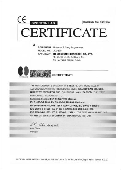
12 1.3 ALL-100/P/G Specification Device Support Pin Count : from 8 pins up to over 300 pins Device Type: EPROM,EEPROM,Serial PROM, FLASH, PLD/CPLD/FPGA, MPU/MCU, etc. Device Contact Default : DIP48,Textool Others: SOP,TSOP,PLCC,QFP,MLF,SDIP etc. through optional CONVERTERs or ADAPTERs Max Sockets in parallel 8 sockets on optional GANG Programming Module Controller 16 bits high-speed controller with big sized FPGA & CPLD Interface Port 1 x USB port Data Transfer Rate USB 1.1 : 12 Mb/s USB 2.0 : 480 Mb/s Max Sites in parallel up to 8 via tiered star USB Functions Load file,read Master,Program,Verify,Auto,ID Check, Checksum,Blank Check,Erase,Protect/Unprotect, Secure,Edit,Function Configuration,Self Test Host Computer Requirements An Intel Pentium or compatible processor with 64MB of RAM At least one USB port available ( V 1.1/ 2.0 ) 20 MB free hard disk space with Windows 98/Me/ 2000/XP/Server 2003 operating system CD-ROM Drive Power AC voltage : VAC Frequency : Hz Power consumption : 50W Dimension L x W x H : 260mm x 150mm x 100mm Weight 4 kg Operating Temperature 0-40 ( ) Safety Standards CE Approved 4
13 1.4 ALL-100G4 Specification Device Support Pin Count : from 8 pins up to over 300 pins Device Type: EPROM,EEPROM,Serial PROM, FLASH, PLD/CPLD/FPGA, MPU/MCU, etc. Device Contact Default : DIP48,Textool Others: SOP,TSOP,PLCC,QFP,MLF,SDIP etc. through optional CONVERTERs or ADAPTERs Max Sockets in parallel 8 sockets on optional GANG Programming Module Controller 16 bits high-speed controller with big sized FPGA & CPLD Interface Port 1 x USB port Data Transfer Rate USB 1.1 : 12 Mb/s USB 2.0 : 480 Mb/s Max Sites in parallel up to 2 via tiered star USB Functions Load file,read Master,Program,Verify,Auto,ID Check, Checksum,Blank Check,Erase,Protect/Unprotect, Secure,Edit,Function Configuration,Self Test Host Computer Requirements An Intel Pentium or compatible processor with 64MB of RAM At least one USB port available ( V 1.1/ 2.0 ) 20 MB free hard disk space with Windows 98/Me/ 2000/XP/Server 2003 operating system CD-ROM Drive Power AC voltage : VAC Frequency : Hz Power consumption : 200W Dimension L x W x H : 300mm x 680mm x 120mm Weight 10.5kg Operating Temperature 0-40 ( ) Safety Standards CE Approved 5
14 2. Single ALL-100/P/G/G4 Installation 2.1 Hardware Installation Before installation, make sure your PC has USB 1.1/2.0 port which can be connected to ALL-100/P/G/G4 Programmer through USB cable. Suggest to use USB 2.0 for fast data transmission with ALL-100/P/ G/G4 Programmer. USB 1.1 (Full Speed) USB 2.0 (High Speed) : Transmission rate 12 Mb/s : Transmission rate 480 Mb/s 6


15 2.1.1 ALL-100/P/G Hardware Installation Step 1: Make sure power of Base Unit is in OFF state and then positioning and connecting Programming Module onto Base Unit. See figures below: 7

16 Step 2: Connect programmer and PC as figures below. Connect the Type B end of USB cable to the USB Type B connector at rear panel of programmer, connect the Type A end of USB cable to the USB Type A connector on the PC. USB type-b connector ALL-100/P/G rear panel 8
17 Step 3: Connect power cable to AC power socket of ALL-100/P/G Programmer and plug in the other end to the outlet of power source ( VAC / Hz). Power on the ALL-100/P/G from the switch above the AC power socket on the rear panel. AC power switch AC power socket 9
18 2.1.2 ALL-100G4 Hardware Installation Step 1: Make sure power of Base Unit is in OFF state and then positioning and connecting Programming Module onto Base Unit. See figures below: 10
19 Step 2: Connect the Type B end of USB cable to the USB Type B connector at rear panel of programmer, connect the Type A end of USB cable to the USB Type A connector on the PC. USB type-b connector ALL-100G4 rear panel 11
20 Step 3: Connect power cable to AC power socket of ALL-100G4 Programmer and plug in the other end to the outlet of power source ( VAC / Hz). Power on the ALL-100G4 from the switch above the AC power socket on the rear panel. AC power switch AC power socket ALL-100G4 rear panel 12
21 2.2 USB Driver Installation Insert the Driver Files CD into CD drive, connect USB cable between PC and ALL-100/P/G/G4, power on ALL-100/P/G/G4 Programmer, the PC will detect the new hardware and a window will open showing Add New Hardware Wizard with information... USB 2.0 Device.... Click Next to continue. To do installation under Windows 2000/XP/Server 2003, user needs to change Log-in authority to Administrator or Power-User in order to install new software/hardware driver. 13
22 Select Search for the best driver for your device Click Next to continue. 14
. Click Next to continue.")
23 Select CD-ROM drive (Insert Driver Files CD into CD drive). Click Next to continue. 15

24 PC will allocate files named ALL100.INF and ALL100.SYS for installation. Click Next to continue. 16

25 Windows has finished the USB driver installation for ALL-100/P/G/ G4 Programmer. Click Finish to complete USB driver installation. 17

26 2.3 Software Installation Insert Driver Files CD to CD-ROM drive, go to directory of ALL-100 under File Manager to execute the SETUP.EXE file, or run the SETUP.EXE from START menu of WINDOWS and follow all steps accordingly as follows: 18

27 Check of installed software: (1) Check if software is installed properly with File Manager, see if XACCESS.EXE, individual IC programming driver, and Utility files exist under C:\Program Files\ALL-100 directory. XACCESS.EXE is a system file which provides an easy way to select IC Manufacturer, Product Type, and the corresponding programming driver. All the programming drivers can also be executed without running XACCESS. EXE file. Each programming driver usually supports a series of relevant ICs. For instance, driver file W28F.EXE is able to program 27C128 ~ 27C512 EPROMs. (2) When executing programming driver, software will automatically check if ALL-100/P/G/G4 Programmer is properly connected. If software can not recognize the existence of ALL-100/P/G/G4, the connection and/or installation might have problem and ALL-100/P/ G/G4 Programmer might not be able to be accessed. (3) Methods to check if ALL-100/P/G/G4 Programmer is properly connected/existed: 1. Run USB Info. option under XACCESS menu. 2. Run programming driver file under XACCESS menu. 19

28 XACCESS.EXE Utility Dialog Box XACCESS.EXE Information Box 20
29 3. ALL-100/P/G/G4 Basic Operation 3.1 Getting Started We will have a brief description of ALL-100 basic operation, introduce how to access the desired IC programming driver through XACCESS, the main system program. We will also introduce functions of Device, Load, Blank check, and Program by taking AMD AM29F200B as example. For best view of ALL-100 information displayed, user s screen should have resolution 800x600 pixels or above Start with XACCESS Click the icon of XACCESS to activate XACCESS.EXE and get following display on the window. 21

30 3.1.2 Select IC Manufacturer Click Device to display IC Manufacturer options. Select AMD and click OK to display Type List of the selected manufacturer. 22
31 3.1.3 Select IC Product Group and Product Type Select EEPROM in Product Group at left side and select AH29F200B in Product Type at right side of Type List Dialogue Box and then click Run. Main Menu of the Driver File Main Menu of the Driver File contains three major parts, the first row for menu of main fuctions, the second row for quick function keys, and the rest provides space for dialogue boxes of IC information like IC Manufacturer, Product Type, Adapter needed... etc. 23

32 The driver file can be executed without going through XACCESS. In main menu of the driver file, user can reselect IC Manufacturer and Product Type. For example, execute driver file XA28F.EXE directly and click Device to select IC Manufacturer and Product Type to be programmed. See dialogue boxes below. Remark: When reselecting IC manufacturer and Product Type, information in dialog box will be updated accordingly and the driver file will be downloaded to ALL-100 Programmer. If message File not found appears, it means the driver file is not available in PC, check the attached Driver File CD or visit HI-LO web site at for S/W download. If a specific ADAPTER is needed, File not found might be due to the absence of the required ADAPTER S/W. Try to install the S/W again. 24

33 3.2 Load file to Programmer buffer It is ready for IC programming after selecting IC Manufacturer and Product Type. In general, programming code is saved in a file in Bin/Hex format. This code needs to be loaded to programmer buffer and then programmed into Blank IC devices. To load file to programmer buffer, click File menu, select Load file to Programmer buffer option, following dialogue box will appear: Function of file loading is similar to that under Windows environment. Enter the file name to be downloaded and click Open, the named file will be loaded to programmer buffer. Note: Disk drive and file path must be correct. Select and click the correct drive and folder that the file located to. If it can not be operated by mouse, apply <TAB>, <UP>, <DOWN>, and <ENTER> keys for selecting and confirming. 25

34 3.3 Read contents from Master IC to buffer When programming code is stored in a Master IC, insert the Master IC onto socket, click Read button on screen or press R key on keyboard to read programming code from Master IC to programmer buffer. When insert Master IC onto socket, make sure Pin 1 orientation and Pin count positioning is correct as diagram indicated. 26

35 pin 1 Caution! Incorrect IC positioning might cause IC damage or be programmed to an unknown state. 27
36 3.4 Program buffer contents to IC Insert IC to be programmed onto socket, click Auto button on screen or press A key on keyboard, following dialogue box will appear. Click Run button on screen or Y key on keyboard or YES on programmer to start programming buffer contents to blank IC. After programming, system will automatically verify data read from programmed IC with data in programmer buffer. If both data match then the GOOD LED will be lit to show a successful programming. For next IC programming, the BUSY LED needs to be off and then insert blank IC onto socket, click Run button on screen or Y on keyboard or YES on programmer to continue programming. Click Close button on screen or <ESC> key on keyboard to go back to main menu. 28
37 3.5 ADAPTERs and CONVERTERs Adequate ADAPTERs and CONVERTERs are available to support various IC types and packages in market such as PLCC, SOP, TSOP, QFP, PGA,... etc. ADAPTER: Each ADAPTER has 40/48 gold plated pins in DIP layout which can be inserted onto 48 pins ZIF socket on the Programming Module.Each ADAPTER has one (or more) programming file(s) that needs to be loaded to the same directory as XACCESS. CONVERTER: CONVERTER is used to convert signals from DIP package to others like PLCC, SOP, TSOP,...etc. No extra programming file is needed to work with CONVERTER. 29

38 3.5.1 ADAPTER and CONVERTER installation S/W Installation: Copy the ADAPTER file(s) attached to the same directory as that for XACCESS file(s). H/W Installation: Insert the DIP-layout 40/48 pins of ADAPTER or CONVERTER onto the 48 PIN DIP ZIF socket on the Programming Module and lock it.see diagram below: 30

39 4. Multiple ALL-100/P/G/G4 Installation USB interface provides functions like Plug-and-Play, auto detection, high expansibility, and high transmission rate (480 Mb/s for 2.0 version). By using these functions, ALL-100/P/G/G4 can be installed up to 8 sets and running simultaneously. After single ALL-100/P/G/G4 installation, more ALL-100/P/G/G4 Programmers can be installed through either extra USB ports of your PC or USB 2.0 Hub like following diagram. Multiple ALL-100 installation through USB 2.0 Hub 31
 are running programming. Site # setting switch is located on the rear panel of ALL-100/P/G/G4 Programmer.")
40 4.1 Multiple ALL-100/P/G/G4 Operation Multiple ALL-100/P/G/G4 operation can increase programming throughput. With Multi-Thread methodology, each programmer can operate independently. The diagram below shows there are two ALL- 100/P Programmers (Site #0 and Site #1) are running programming. Site # setting switch is located on the rear panel of ALL-100/P/G/G4 Programmer. Valid Site # for Multiple ALL-100/P/G/G4 setup is 0~7 and can not have the same Site # in whole system. Site # setting 32
41 When running ALL-100/P/G/G4 programming software, system will automatically detect and load necessary driver S/W and also download programming code to ALL-100/P/G/G4 through USB port. Operation of multiple ALL-100/P/G/G4 is basically the same as that of single ALL-100/P/G/G4. There are two operation modes for multiple ALL-100/P/G/G4 programming, synchronous operation and asynchronous operation. After entering programming mode on screen, user can choose either of following two operation modes depending on production needs: Synchronous operation: Run programming on all the ALL-100/P/G/G4 at the same time. Put ICs onto socket of each ALL-100/P/G/G4, press Y key on PC keyboard. All ALL-100/P/G/G4 will start programming simultaneously. Asynchronous operation: Run programming on each ALL-100/P/G/G4 one after another. Put IC on the 1st ALL-100/P/G/G4, press <YES> on that programmer to start programming, then put another IC on the 2nd ALL-100/P/G/G4, press <YES> on that programmer to start programming, then the 3rd one... and so on. 33
42 4.2 Read/Compare on Multiple ALL-100/P/G/G4 To perform Read/Compare function under Multiple ALL-100/P/G/G4 setup, only Site #0 is valid. This means that only IC on Site #0 can be read/compared under Multiple ALL-100/P/G/G4 setup. Read Dialogue Box 34

43 Compare Dialogue Box 35
44 5. ALL-100G/G4 Gang Option Installation For further speed up programming for volumes of ICs, 8 sockets Programming Module option is available. Contact your local HI-LO agent for ordering information. ALL-100G/G4 Gang Programmer is an ALL-100G/G4 Base Unit with 8 sockets Programming Module put on the top. User can choose either Single ALL-100G/G4 Gang operation or Multiple ALL-100G/G4 Gang operation for mass programming. The S/W attached with 8 sockets Programming Module is used for ALL-100G/G4 Gang as well as Multiple ALL-100G/G4 Gang operation. The installation /operation is similar as what is stated above. Due to more information to be displayed on screen for Gang operation, user s screen resolution needs to be 1024x768 pixels (SVGA mode) or above. 36


45 37
 is running programming.")
46 5.1 ALL-100G/G4 Gang Operation ALL-100G/G4 Gang Programmer ties IC pin count in parallel, drive programming and control signals through FPGA to program ICs on all sockets simultaneously. The diagram below shows there is one ALL- 100G/G4 Gang Programmer (Site #0) is running programming. ALL-100G/G4 Site # ALL-100G/G4 Gang x8 sockets Up to 8 sets of ALL-100G/G4 Gang Programmer can be connected to PC through USB interface, this is so call Multiple ALL-100G/G4 Gang Setup. Each ALL-100G/G4 Gang can program 8 ICs. One PC with 8 sites of ALL-100G/G4 Gang setup can program 8x8= 64 ICs. 38
 of the 1st site (Site #0) Gang Programmer can be read/compared under Multiple ALL-100G/G4 Gang setup.")
47 5.2 Read/Compare on Multiple ALL-100G/G4 Gangs To perform Read/Compare function under Multiple ALL-100G/G4 Gang operation, only IC on MASTER (Socket #1) of Site #0 Gang programmer is valid. This means that only the 1st IC on MASTER (Socket #1) of the 1st site (Site #0) Gang Programmer can be read/compared under Multiple ALL-100G/G4 Gang setup. Put IC to be read/compared onto MASTER (Socket #1) of Site #0 Gang Programmer and click Read/Compare keys on screen. Refer paragraph 4.1 for setting of Site # for Gang Programmer. 39

48 6. ALL-100/P/G/G4 Software Description 6.1 XACCESS User Interface System Software XACCESS is an interface guiding user to locate the driver software for product type to be programmed. XACCESS also provides File Management Utilities as well as Data Base of programmable IC products. Functional memu Fast key Fast open IC Manufacturer 40
49 6.2 Utilities: File Management Utilities includes Hex to Bin Converter, Bin to Hex Converter, 2-way splitter, 4-way splitter, 2-way shffler, and 4-way shuffler,...etc Hex to Bin Converter Convert data from Hex format to Binary format for programmer Read/ Write. Binary file name to convert to Hex file name to be converted Hex to Bin Converter Hex format option Start/end address Contents of Unused Bytes 41

50 6.2.2 Bin to Hex Converter Convert data from Binary format to Hex format. Hex file name after convert Binary file name before convert Bin to Hex Converter Hex format option Binary Input Start Add. Hex output Start Add. 42
 or Double")
51 way splitter Split one file into two output files. One file contains odd-byte data of the original file and the other file contains even-byte data of the original file. Filenames after split Filename to be splitted 2-way splitter Split format options Split Data Format: Normally the split data is in Byte Wide, however, user can choose Word Wide (two bytes) or Double Word Wide (four bytes) as unit of data split. 43

52 way splitter Split one file into four output files. The 1st file contains the 1st byte of every 4-byte data segment of the original file. The 2nd, 3rd, and 4th file contains the 2nd, 3rd, and 4th byte of every 4-byte data segment of the original file. Filenames after split Filename to be splitted 4-way splitter Split format options Split Data Format: Normally the split data is in Byte Wide, however, user can choose Word Wide (two bytes) or Double Word Wide (four bytes) as unit of data split. 44
")
53 way shuffler Combine two files into one. Insert data of Even file into even byte position of the combined file and insert data of Odd file into odd byte position of the combined file. Filenames to be shuffled Filename after shuffle 2-way shuffler Shuffle format options Shuffle Data Format: Normally the shuffled data is in Byte Wide, however, user can choose Word Wide (two bytes) or Double Word Wide (four bytes) as unit of data shuffle. 45

54 way shuffler Combine four files into one. Insert data of 1st file into the 1st byte of every 4-byte data segment of the combined file, insert data of 2nd, 3rd, and 4th file into the 2nd, 3rd, and 4th byte of every 4-byte data segment of the combined file. Filenames to be shuffled Filename after shuffle 4-way shuffler Shuffle format options Shuffle Data Format: Normally the shuffled data is in Byte Wide, however, user can choose Word Wide (two bytes) or Double Word Wide (four bytes) as unit of data shuffle. 46

55 6.2.7 Version List List version number of current programming software. Name of programming software Version Version List 47

56 6.2.8 Cross Reference List the Cross Reference of IC Mfr., Product Type, and the corresponding programming software. IC Mfr. Programming Software IC Product Type Adapter if needed Cross Reference 48

57 6.2.9 Device List List all device types that are programmable at current version. Print out the list Save the list Device List IC Product Type 49
58 6.3 Programming Data/ Function Description Programming software includes loading of programming driver, utilities of data management, and control of programming function/operation. Each programmable IC needs correct functional setup before programming. User needs to refer IC data sheet and/or application software for proper setup of programming function. See description below by taking AMD AM29F200B IC as example. Functional menu Fast key Selected IC Mfr. and Product Type Adapter needed Programming addresses Checksum of programming data Size of programming buffer Location of programming buffer Status indicator Programming progress indicator 50
59 6.3.1 File Load/Save of data file and configuration file. See dialogue boxes below. Functional menu 51

60 (1) Dialogue boxes of load data file: Data file to be loaded File format options File format options Data of Unused Bytes File addresses setting 52

61 (2) Dialogue box of save data file: Data file to be saved File format options (3) Dialogue boxes of load/save Programming Configuration file: The Programming Configuration file contains all programming related data setup by user. It includes programming driver, data file, programming functional setting, and serial number setting. User can save Programming Configuration file for load it back next time for programming without re-setting of programming function and serial number. 53
62 Programming Configuration file to be loaded Programming Configuration file to be saved 54
63 (4) Dialogue box of enable Job Function: Once user enable Job Function and followed by loading Programming Configuration file, system will enter <AUTO> programming mode and is ready for programming. User needs not re-do the programming functional setting and serial number setting. Enable Job Function 55
64 6.3.2 Edit Includes edit and address of programming data. See dialogue box below. Edit programming data option Address programming data option 56
65 (1) Edit data: Provide functions such as Fill, Jump, Swap, Calc, SUM, Search,... etc for user to edit programming data in Hex and ASC II expressions. Edit functional menu Current address Hex data ASCII data 57
66 (2) Fill: Specify start and end addresses and data to be filled in, then click OK, data will be filled into the specified area. 58
67 (3) Jump: Specify the start address to jump to, then click OK, system will jump to the specified address with data displayed. 59

68 (4) Move: Specify start and end addresses in which data to be moved, also specify the destination address to move to, then click OK, system will move data between spcified addresses to the destination area. 60
69 (5) Swap - Byte: Specify start and end addresses in which data to be byte-swaped, then click OK, system will swap byte for data between specified addresses. 61
70 (6) Swap - Nibble: Specify start and end addresses in which data to be nibble-swaped, then click OK, system wil swap Nibble for data between specified addresses. 62
 on")
71 (7) CalcSum: Specify start and end addresses in which data to be calculated for checksum and then click OK, system will calculate and display result (checksum) on screen. 63
72 (8) Search: Two options available, search ASC II data or search Binary data. 64
73 Specify start/end addresses and data to be searched, then click OK, system will search data between specified addresses and list all addresses that match data to be searched. 65
74 (9) Print: Two options available, print to printer or ouput to file. 66

75 Specify start/end addresses and then click OK, system will print/ save data between specified addresses to printer/output file. 67
76 (10) Modify Programmer Buffer Mapping: Set Buffer programming addresses Set Device programming addresses 68
77 Example: Program data from Buffer address $ $0FFFF to Device address $ $1FFFF. Start...End Device : Buffer : FFFF 0FFFF $00000 $00000 $0FFFF $10000 $0FFFF $10000 $1FFFF $1FFFF Programmer Buffer Device 69
78 6.3.3 Operation Different IC product type might have different options of programming functions. Basically, programming functions include options of Erase, Blank, Program, Verify, Lock, Auto,...etc. Functional options for Device AM29F200B User can also click <Fast Key> to excute program functions. See <Fast Key> indicated below: Fast key for Device AM29F200B 70

79 (1) Read: Read contents in IC memory. Read function is only valid for IC on following position. Single ALL-100/P/G/G4 setup: The IC on the socket. Multiple ALL-100/P/G/G4 setup: The IC on socket of Site #0 programmer. Single ALL-100/P/G/G4 Gang setup: The IC on Socket #1 of Gang programmer. Multiple ALL-100/P/G/G4 Gang setup: The IC on the 1st Socket (Socket #1) of the 1st Site (Site #0) Gang programmers. Read options IC ID Check Process status and Message After Read operation, suggest user to double-check to confirm checksum and the data read are all correct. 71
80 (2) Auto: Enter programming mode with all programming functions activated. Sector/Block setting Parameter setting Programming functional options IC Mfr./Protect type Checksum result button Programming result Process status Reset button Different IC product type might have different programming functional setting and parameter setting. User needs to refer IC data sheet for proper settings of programming functions and programming parameters. 72


81 Sector/Block: Specify Sector/Block to be protected if needed. Parameter: Special setting for programming if needed. 73
82 Result button: Button to display programming result and elapsed time. Result button 74
83 (3) Erase : Enter programming mode with Erase function activated. Blank : Enter programming mode with Blank check activated. Program : Enter programming mode with Program function activated. Verify : Enter programming mode with Verify function activated. Protect : Enter programming mode with Protect function activated. Blank Check option ID Check option 75

84 Program & Verify options ID Check option 76

85 6.3.4 USB Info. Display current ALL-100/P/G/G4 connection status through USB interface. ALL-100 connection status 77

86 6.3.5 About Display model number of current programmer and version number of programming driver. Version number of programmer and driver 78
87 7. ALL-100/P/G/G4 Troubleshooting After power on, ALL-100/P/G/G4 will run self diagnostics and USB connection check. Green/Red LED will display test result. Table listed below summarize test result with possible causes/dispositions for troubleshooting. Condition After power on, Green and Red LED off. After power on, Green and Red LED flash. After power on, Green LED off but Red LED flash. After power on or during programming, Green LED flash but Red LED off. During programming, Greend LED on but Red LED flash. During programming, Green LED on but Red LED become orange color. Possible cause/dispositions Poor contact / operation abnormal: 1. Check power cable connection. 2. Need troubleshooting. Contact your local dealer for service. Fail self diagnostic test: 1. Check if there is IC on socket (Should be removed). 2. Need troubleshooting. Contact your local dealer for service. Fail ALL-100 memory diagnostic test: 1. Try to power on again. 2. Need troubleshooting. Contact your local dealer for service. Fail USB connection check: 1. Check USB cable connection. 2. Check PC BIOS setup to see if USB is disabled (Should be enabled). 3. Need troubleshooting. Contact your local dealer for service. USB communication error: 1. Check USB cable connection. 2. Need troubleshooting. Contact your local dealer for service. USB data trasmission interrupted: 1. Check USB cable connection. 2. Check if PC is interrupted. 3. Need troubleshooting. Contact your local dealer for service. 79
88 8. Glossary 8.1 EPROM, EEPROM, BPROM, and MPU Programmable device: An integrated circuit (IC) that can be programmed. Bit, Nibble, Byte, Word, Double Word Bit : A basic unit of binary data. Nibble : A groug of 4-bit binary data. A nibble ranges from 0H to FH. Byte : A group of 8-bit binary data. A byte ranges from 0H to FFH. Word : A group of 16-bit binary data. A word ranges from 0H to FFFFH. Double word : A group of 32-bit binary data. A double word ranges from 0H to FFFFFFFFH. Buffer There is 4 Mbit memory buffer in ALL-100/P/G/G4 Programmer. IC driver file can automatically allocate/arrange these 4Mbit memory space for programming depending on IC memory size and read/write needs. When data needs to be programmed to IC, data needs to be loaded to programmer buffer first and then program to IC. When data is read from Master IC, the data is also stored in programmer buffer, it can then be edited or saved to disk for future use. 80
89 Buffer Start and Buffer End Address It specifies the start and end addresses in programmer buffer in which data is to be programmed to IC in sequence. This is also the area that data is used for Checksum calculation. CheckSum This is the SUM of all data contents between buffer start and buffer end addresses. All data are added and the least significant 16 bits (4 HEX) are displayed as the Checksum. (Some data in some ICs might not be covered in Checksum calculation.) Checksum will be calculated after IC reading, file loading, type changing, or buffer editing. Bit Count of data A NIBBLE contains 4-bit data. A BYTE contains 8-bit data. A WORD contains 16-bit data. MPU is normally in 8 or 16 bit width, but still have some in 12 or 14 bit width. Device Start and Device End address It specifies the start and end addresses inside IC device. During IC programming, data stored in programmer buffer will be written to this specified area. 81
90 USB interface USB, Universal Serial Bus, is a high speed data transmission bus initiated by Intel and then supported by NEC, IBM, MicroSoft, Compaq,...etc. It is now a data transmission standard between PC and peripheral devices. V1.0 / 1.1 USB Low-Speed : 1.5 Mb/s V1.0 / 1.1 USB Full-Speed : 12 Mb/s V2.0 USB High-Speed : 480 Mb/s Security fuse Security fuse is available in most of programmable ICs. Once the Security fuse has been blown, the data stored in IC can not be read out correctly and IC can not be programmed either. However, IC can still operate functionally no matter the Security fuse has been blown or not. Note: Once the Security fuse has been blown. IC data can no longer be read out or programmed correctly, please double-check before programming Security fuse. Lock bits Some MCU/MPU use Lock bits to protect data programmed. Normally user has options to select individual Lock bit to protect different area of memory data. Please refer IC data sheet for definition of Lock bits. 82
91 Encryption Some MCU/MPU use Encryption code for data protection. If an IC has been programmed with Encryption code, then a correct decryption code must be given to read the correct data. Protection Fuse Some FLASH memory use Protection fuse for data protection. It can prevent data change from accident programming. The Protection fuse must be reset to Unprotection state, if the programmed data need to be changed. The default state of Protection fuse is Unprotection. 83
92 8.2 PLD, PAL, GAL, PEEL, CPLD, EPLD, and FPGA Programmable Logic Device (PLD) PLDs are usually grouped into following five categories: PLD : A one time Programmable Logic Device such as PAL. EPLD : A UV Erasable PLD such as EPLD, CPLD, and FPGA. These devices have transparent window on top of package for UV light exposure. EEPLD : An Electrically Erasable PLD such as GAL, PEEL, CPLD, and FPGA. CPLD : A more complex PLD device. FPGA : Field Programmable Gate Array. JEDEC fuse map file of PLD JEDEC fuse map file is a standard format used for PLD programming. It contains fuse information and functional test vectors of PLD to be programmed. Most PLD assemblers or compilers such as PALASM, OPAL, CUPL, ABEL, AMAZE, and PDK-1, can create JEDEC fuse map file. POF fuse map file of PLD POF fuse map file is a format used for ALTERA PLD programming. POF file can store more programming data than JEDEC file. 84
93 Fuse blown and intact Most of unprogrammed (blank) PLD have fuses in intact (connect) state. After programming, PLD fuses are blown to open state. For one time programmable PLD, once fuses are blown (opened), they can not be changed back to intact (connect) state. However, the UV erasable PLD can be erased to change fuses back to intact (connect) state by UV light exposure and the electrically erasable PLD can be electrically erased to change fuses back to intact (connect) state by using Erase function on this Programmer. Array fuse, Configuration fuse Array fuses are the main logic fuses in a PLD. Different types of PLD have different logic function arrangement. Configuration fuses define the I/O architecture of a PLD such as Combinatorial/Registered, Output feedback/output enable, and so on. Generally, user do not have to understand the details of these fuses because logic compiler will automatically translate logic statements and equations into JEDEC format file. Security fuse Most of PLD have Security fuse. Once Security fuse is blown, data in PLD can no longer be read out correctly. Generally, the PLD will be read as blank if Security fuse is blown. 85
94 Note: 86
95 87
ALL-200G. Universal Gang Programmer. User s Manual
 ALL-200G Universal Gang Programmer User s Manual Apr. 2014 Caution : USB Interface Compatibility For USB 2.0 compatibility, your computer should work with the following operation system or later revision
Pin-Master 48. Everything you need from a development programmer
 Pin-Master 48 Everything you need from a development programmer Device Types Over 8750 device types Includes 3V parts EPROMs, EEPROMs, FLASH EPROMs and Emulators up to 48 pins PLDs and FPGAs including
Dataman-S6 - User's Manual. Dataman-S6 Compact USB Programmer User's Manual
 Dataman-S6 Compact USB Programmer User's Manual Contents Chapter 1 Product Description 1-1 Introduction 1-2 Safety Information 1-3 Precautions 1-4 Operating System, Hardware Requirements 1-5 Accessories
MP8011A. Gang Programming System
 MP8011A Gang Programming System User s Manual Copyright 2000 SofTec Microsystems DC00242 SofTec Microsystems via Roma, 1 33082 Azzano Decimo (PN) ITALY Tel: (+39) 0434 640 729 Fax: (+39) 0434 632 695 E-mail
XELTEK Superpro E Series
 User s Guide XELTEK Superpro 6000-6000E Series Ultra-Fast, Stand-Alone, 144pin Programmer of the Future XELTEK 1296 Kifer Rd. Unit 605 Sunnyvale, CA 94086 Tel: (408) 530-8080 Fax: (408) 530-0096 www.xeltek.com
 WWW.LOGICALDEVICES.COM Table of Contents Welcome... 6 Feature Highlights... 6 User Manual Organization... 7 Chapter 1 General Description... 8 Introduction to XPRO... 8 Package Contents... 8 Software Features...
Standard Accessories. Install software and driver. Introduction. Caution
 Standard Accessories LEAPER-3D FLASH WRITER main unit x1, USB cable x1, DC 12V/500mA adaptor x1, PC Software, drivers and manual on CD-ROM x1 Introduction Main unit Unit top view IC package diagram Adaptor
XELTEK Superpro 7500 Series
 User's Guide XELTEK Superpro 7500 Series Ultra Fast, Stand Alone, 144pin Programmer of the Future XELTEK 1296 Kifer Rd. Unit 605 Sunnyvale, CA 94086 Tel: (408) 530 8080 Fax: (408) 530 0096 www.xeltek.com
Programmable Logic Devices I. EECE143 Lecture 4. PALs, GALs & CUPL. A lesson on Programmable Logic Devices and programming them using CUPL
 PALs, GALs & CUPL A lesson on Programmable Logic Devices and programming them using CUPL What is Programmable Logic? Digital integrated circuits where the Boolean function can be determined by the user.
XELTEK Superpro 7000 Series
 User s Guide XELTEK Superpro 7000 Series Ultra Fast, Stand Alone, 144pin Programmer of the Future XELTEK 1296 Kifer Rd. Unit 605 Sunnyvale, CA 94086 Tel: (408) 530 8080 Fax: (408) 530 0096 www.xeltek.com
LABTOOL-T400. Turbo Flash Gang Programmer. User's Manual
 LABTOOL-T400 Turbo Flash Gang Programmer User's Manual Copyright Notice This document is copyrighted, 1998-2006 by Advantech Equipment Corp., Ltd. All rights are reserved. Advantech Equipment Corp., Ltd.,
Advin Systems Inc. PILOT DEVICE PROGRAMMERS User's Manual. Legal Notices. Life Support Policy. Warranty Information
 Legal Notices Advin Systems Inc. PILOT DEVICE PROGRAMMERS User's Manual The information contained in this manual has been carefully checked and is believed to be accurate and complete at the time of printing.
Galep-4 Universal Programmer [ Parallel Port ]
![Galep-4 Universal Programmer [ Parallel Port ]](/thumbs/94/119484089.jpg "Galep-4 Universal Programmer [ Parallel Port ]") Galep-4 Universal Programmer [ Parallel Port ] PALMSIZED, 40 PIN PROGRAMMER Device Support: By name: 5,825. By package: 12,330 Dual power (AC adapter plus internal battery w/8 hours continuous operation
Galep-4 Universal Programmer [ Parallel Port ] PALMSIZED, 40 PIN PROGRAMMER Device Support: By name: 5,825. By package: 12,330 Dual power (AC adapter plus internal battery w/8 hours continuous operation
1. INTRODUCTION GETTING STARTED / INSTALLATION... 10
 1. INTRODUCTION... 7 PROGRAMMER MODELS FOR PC USB INTERFACE... 7 PROGRAMMER MODELS FOR PC USB INTERFACE WITH MULTI-SOCKETS... 7 DISCONTINUED PROGRAMMER MODELS... 8 ABOUT THIS MANUAL... 8 GENERAL DESCRIPTION...
PCI to SH-3 AN Hitachi SH3 to PCI bus
 PCI to SH-3 AN Hitachi SH3 to PCI bus Version 1.0 Application Note FEATURES GENERAL DESCRIPTION Complete Application Note for designing a PCI adapter or embedded system based on the Hitachi SH-3 including:
Programmer. User Guide
 Programmer User Guide Trademarks & Copyright Windows and Windows NT are registered trademarks of Microsoft Corporation. MCS-51 and Pentium are registered trademarks of Intel Corporation. AVR is registered
User's Guide COPYRIGHTS. For Windows 95/98/NT/2000. SUPERPRO Series Universal Programmers
 SUPERPRO Series Universal Programmers For Windows 95/98/NT/2000 User's Guide COPYRIGHTS Software Copyrights User's Guide Copyrights 1997-2006 XELTEK 1997-2006 XELTEK This software product is copyrighted.
Microprocessors and Microcontrollers (EE-231)
") Microprocessors and Microcontrollers (EE-231) Main Objectives 8088 and 80188 8-bit Memory Interface 8086 t0 80386SX 16-bit Memory Interface I/O Interfacing I/O Address Decoding More on Address Decoding
Microprocessors and Microcontrollers (EE-231) Main Objectives 8088 and 80188 8-bit Memory Interface 8086 t0 80386SX 16-bit Memory Interface I/O Interfacing I/O Address Decoding More on Address Decoding
Note: In order to connect the programmer easily and quickly, please connect the hardware after installing the software.
 Note: In order to connect the programmer easily and quickly, please connect the hardware after installing the software. Copyrights Software Copyright 2003-2008 XELTEK User's Guide Copyright 2003-2008 XELTEK
FLASH PROGRAMMER FP-8903 VER 2.00 USER S MANUAL
 FLASH PROGRAMMER FP-8903 VER 2.00 USER S MANUAL FP8903 V2.00 DOC R.2.0 1 TABLE OF CONTENTS SECTION CONTENTS PAGE 1 INTRODUCTION 1.1 MANUAL CONTENTS 03 1.2 PROGRAMMER AND ACCESSORIES 03 2 FEATURES 04 3
1. General Description
 Note: In order to connect the programmer easily and quickly, please connect the hardware after installing the software. Copyrights Software 2003-2008 XELTEK User s Guide Copyright Copyrights 2003-2008
XELTEK Superpro 7000 Series
 Userʹs Guide XELTEK Superpro 7000 Series Ultra Fast, Stand Alone, 144pin Programmer of the Future XELTEK Zijin (Jiangning) Technology Incubation Special Park, Jiangning, Nanjing, P.R.China 2111011 +86-25-68161208
User s Manual. Tianjin Weilei Techonlogy Ltd. 天津威磊电子技术有限公司
 User s Manual www.weilei.com Tianjin Weilei Techonlogy Ltd. 天津威磊电子技术有限公司 1. Introduction The WELLON Programmers are affordable, reliable, and fast universal device programmers. They are designed to operate
OVERVIEW ChipMax2 With high throughput and maximum flexibility Maxloader
 OVERVIEW ChipMax2 is a high-speed universal device programmer for USB 2.0 PC-interface. It programs a 64Mbit flash memory in 42 seconds. This is a true low-price production oriented system. The ChipMax2
BIPOLAR PROM ADAPTER READ THIS SHEET FIRST!
 BIPOLAR PROM ADAPTER READ THIS SHEET FIRST! The BIPOLAR PROM ADAPTER (#ABIP) must be used with caution. The addendum which accompanies the adapter describes the precautions which must be followed for the
GANG Programmer for flash micro computers. User s Manual. TESSERA Technology INC. Third Edition September
 GANG Programmer for flash micro computers User s Manual TESSERA Technology INC. Third Edition September 2008-1 - Table of Contents Chapter 1 Summary 3 1.1 System Configuration 4 Chapter 2 Installation
Cover. MATWorX Installation Guide NWA ISSUE 2.1
 Cover MATWorX Installation Guide NWA-008862-001 ISSUE 2.1 LIABILITY DISCLAIMER NEC Corporation reserves the right to change the specifications, functions, or features, at any time, without notice. NEC
ZCRMZNICE01ZEMG Crimzon In-Circuit Emulator
 Quick Start Guide QS006602-0408 Introduction Zilog s ZCRMZNICE01ZEMG Crimzon (ICE), shown in Figure 1, provides Crimzon chip family emulation with a Trace and Event system for program debugging using Zilog
FlashMaxII Operation Guide
 FlashMaxII Operation Guide 2015-07-09 Version 1.0 EE Tools, Inc. 4620 Fortran Drive Suite 102 San Jose, CA 95134, USA www.eetools.com sales@eetools.com Tel : (408)263-2221 Fax : (408)263-2230 1 Table of
Embedded Controller Design. CompE 270 Digital Systems - 5. Objective. Application Specific Chips. User Programmable Logic. Copyright 1998 Ken Arnold 1
 CompE 270 Digital Systems - 5 Programmable Logic Ken Arnold Objective Application Specific ICs Introduce User Programmable Logic Common Architectures Programmable Array Logic Address Decoding Example Development
More Programming with CUPL
 More Programming with CUPL Compiling PLD File Use WinCUPL or use another text editor to create your file Save your file with the extension.pld Compile using WinCUPL make sure you have no errors. Save your.jed
99 Washington Street Melrose, MA Fax TestEquipmentDepot.com 848A
 99 Washington Street Melrose, MA 02176 Fax 781-665-0780 TestEquipmentDepot.com 848A Introduction 848A is next member of Windows 95/98/ME/NT/2000/XP based B+K PRECISION specialized programmers. Programmer
T9600 Universal Programmer User s Manual
 T9600 Universal Programmer User s Manual Release Notes Version 1.0 Feb. 14th, 2002 Content Technical Support 2 1. Introduction 3 1.1 About this manual 1.2 Product description 1.3 Package content 2. Hardware
iup-200aliup-201a UNIVERSAL PROM PROGRAMMERS
 iup-200aliup-201a UNIVERSAL PROM PROGRAMMERS MAJOR iup-200aliup-201a FEATURES: Personality Module Plug-Ins Provide Industry First Support for Intel and Intel Compatible EPROMs, EEPROMs, KEPROM, Microcontrollers,
8051 INTERFACING TO EXTERNAL MEMORY
 8051 INTERFACING TO EXTERNAL MEMORY Memory Capacity The number of bits that a semiconductor memory chip can store Called chip capacity It can be in units of Kbits (kilobits), Mbits (megabits), and so on
Infrared Docking Station
 For uploading voice files to Enterprise Express Infrared Docking Station Operating Instructions Contents Overview...1 What s In The Box...1 System Requirements...1 Where to Go From Here...3 Getting Help...4
USB Read/Write Memory Adapter MAUSB-300 REFERENCE MANUAL
 USB Read/Write Memory Adapter MAUSB-300 REFERENCE MANUAL Introduction Thank you for purchasing our product. The MAUSB-300 USB Read/Write Memory Adapter (hereinafter referred to as the adapter ) is designed
EMP Monitor Operation Guide V4.30
 EMP Monitor Operation Guide V4.30 Meanings of symbols used The following table shows the symbols used in this manual, along with descriptions of what they mean. Attention s Indicates procedures which may
TOPWIN. Universal Programmer. User Manual
 TOPWIN Universal Programmer User Manual 株式会社秋葉原 AKIHABARA INC. www.aitendo.co.jp 2004.10. Content Brief Introduction... 3 Chapter I Software Installation... 4 1.1 Software Installation... 4 1.2 Hardware
SUPERPRO Series Universal Programmers For Windows 95/98/NT/2000. User Guide XELTEK
 SUPERPRO Series Universal Programmers For Windows 95/98/NT/2000 User Guide XELTEK 1 COPYRIGHTS Software Copyrights 1997-2006 XELTEK User's Guide Copyrights 1997-2006 XELTEK This software product is copyrighted.
MW100 CAN Bus Module Configuration Tool (MX118-CAN-M30/S1) User s Manual
 User s Manual") MW100 CAN Bus Module Configuration Tool (MX118-CAN-M30/S1) User s Manual 1 Contents Before Using the Software... 3 Explanation of Functions... 3 MX118 Part Names and Functions... 3 Operation Guide... 4
MW100 CAN Bus Module Configuration Tool (MX118-CAN-M30/S1) User s Manual 1 Contents Before Using the Software... 3 Explanation of Functions... 3 MX118 Part Names and Functions... 3 Operation Guide... 4
LPT-to-I2C SE. Hardware Reference Guide.
 LPT-to-I2C SE Hardware Reference Guide http://www.i2ctools.com/ November 1, 2008 Information provided in this document is solely for use with the LPT-to-I2C SE product from SB Solutions, Inc. SB Solutions,
Menu. word size # of words byte = 8 bits
 Menu LSI Components >Random Access Memory (RAM) Static RAM (SRAM) Dynamic RAM (DRAM) Read-Only Memory (ROM) Look into my... See figures from Lam text on web: RAM_ROM_ch6.pdf 1 It can be thought of as 1
JUNE 2000 IC136C. USB Card
 USB Card JUNE 2000 IC136C CUSTOMER SUPPORT INFORMATION Order toll-free in the U.S. 24 hours, 7 A.M. Monday to midnight Friday: 877-877-BBOX FREE technical support, 24 hours a day, 7 days a week: Call 724-746-5500
Que! USB Floppy Disk Drive Installation Guide
 Que! USB Floppy Disk Drive Installation Guide status indicator: The status indicator LED lights up to indicate that the floppy disk drive is accessing a floppy disk. disk door: The disk door prevents dust
User s Guide QL-720NW
 User s Guide QL-720NW Be sure to read and understand this guide before using the machine. We recommend that you keep this guide nearby for future reference. Not all models are available in all countries.
RTE for WIN32. Installation Manual (Rev.7.0) Midas lab
 Midas lab") Midas lab REVISION HISTORY Date Revision Chapter Explanation of revision March 11,2000 4.0 RTE4W32 Ver.5.0 (First edition) January 10,2002 4.1 Add Windows XP support (RTE4W32 Ver.5.05) October 29,2002
Midas lab REVISION HISTORY Date Revision Chapter Explanation of revision March 11,2000 4.0 RTE4W32 Ver.5.0 (First edition) January 10,2002 4.1 Add Windows XP support (RTE4W32 Ver.5.05) October 29,2002
SUPERPRO Series Universal Programmers For Windows 95/98/NT/2000. User Guide XELTEK
 SUPERPRO Series Universal Programmers For Windows 95/98/NT/2000 User Guide XELTEK 1 COPYRIGHTS Software Copyrights 1997-2006 XELTEK User's Guide Copyrights 1997-2006 XELTEK This software product is copyrighted.
GANGSTAR PRO-848 GANG PROGRAMMER USER MANUAL
 GANGSTAR PRO-848 GANG PROGRAMMER USER MANUAL LOGICAL DEVICES INC. PO BOX 8400 DENVER, CO 80201 TEL: 303-861-8200 FAX: 303-813-9019 WWW.LOGICALDEVICES.COM Copyright Notice This document is copyrighted,
T/H 9600 Help 1 of About System General 3 2. About T T9600 Product Descriptions T9600 Package Contents 4 2.
 T/H 9600 Help 1 of 50 1. About System General 3 2. About 9600 4 2.1 T9600 4 2.1.1 T9600 Product Descriptions 4 2.1.2 T9600 Package Contents 4 2.2 H9600 Product Descriptions 4 3. Understanding The Hardware
DiskOnChip PCI Evaluation Board
 User Manual DiskOnChip PCI Evaluation Board JANUARY 2002 91-SR-010-04-7L REV 1.1 Table of Contents 1 Introduction... 3 1.1 Supported Devices...3 1.2 Features... 4 2 DiskOnChip PCI EVB Package Contents...
 Distributed by: www.jameco.com 1-800-831-4242 The content and copyrights of the attached material are the property of its owner. Programming Adapters The ChipMax pin driver capability lets it program
CIFER Standards Converter
 CIFER Standards Converter Update Instructions Pro-Bel Ltd Issue: 1.0 Date: April 07 Pro-Bel Ltd Hartman House Danehill Lower Earley Reading Berks, RG6 4PB ENGLAND Web: www.pro-bel.com HU-CIFER-UPDATE 1
User's Manual. USB DOCK - Einstein. Omnidirectional Control Technology Inc.
 User's Manual USB DOCK - Einstein Omnidirectional Control Technology Inc. Index INTRODUCTION...3 SYSTEM REQUIREMENTS...3 PACKAGE CONTENTS...3 CONNECTORS...4 USB DOCK FUNCTIONS...4 LED INDICATOR...5 INSTALLING
mini USB ISDN TA128 User s Manual
 mini USB ISDN TA128 User s Manual Billion mini USB ISDN TA128 CE Approval All CE approved ISDN devices may be connected to the Euro- ISDN in all countries of the EU. Billion mini USB ISDN TA128 has been
FireWire 800+Hi-Speed USB Combo Quick Installation Guide
 FireWire 800+Hi-Speed USB Combo Quick Installation Guide Introducing the FireWire 800+Hi-Speed USB Combo The FireWire 800 + Hi-Speed USB Combo features the latest technology in FireWire 800 and USB 2.0.
MaxLoader User s Guide
 1. INTRODUCTION... 7 PROGRAMMER MODELS FOR PC USB INTERFACE 7 PROGRAMMER MODELS FOR PC USB INTERFACE MULTI-SOCKETS 8 PROGRAMMER MODELS FOR PC PARALLEL INTERFACE 8 ABOUT THIS MANUAL 8 GENERAL DESCRIPTION
Spectrometer Visible Light Spectrometer V4.4
 Visible Light Spectrometer V4.4 Table of Contents Package Contents...3 Trademarks...4 Manual Driver and Application installation...5 Manual Application Installation...6 First Start of the Application...8
1 PC Hardware Basics Microprocessors (A) PC Hardware Basics Fal 2004 Hadassah College Dr. Martin Land
 PC Hardware Basics Fal 2004 Hadassah College Dr. Martin Land") 1 2 Basic Computer Ingredients Processor(s) and co-processors RAM main memory ROM initialization/start-up routines Peripherals: keyboard/mouse, display, mass storage, general I/O (printer, network, sound)
1 2 Basic Computer Ingredients Processor(s) and co-processors RAM main memory ROM initialization/start-up routines Peripherals: keyboard/mouse, display, mass storage, general I/O (printer, network, sound)
Intelligent Universal Programmer User s Manual
 M1881UXP Intelligent Universal Programmer User s Manual Copyright Notice This document is copyrighted, 2000, 2001, 2002 by MINATO ELECTRONICS INC. All rights are reserved. MINATO ELECTRONICS INC. reserves
Chapter 1 Introduction
 Contents Contents...1 Chapter 1 Introduction...2 1. Features...2 2. Package checklist...2 Chapter 2 Installation...3 1. ELAN Display writer...3 2. Hardware requirements...6 3. Hardware Installation...7
Ryerson Polytechnic University Department of Electrical and Computer Engineering ELE 328 Digital Systems and Microprocessors
 Ryerson Polytechnic University Department of Electrical and Computer Engineering ELE 328 Digital Systems and Microprocessors Lab 1 CAD Tools 10 marks (2 Weeks) Fall 2002 Due Date: Week 4 Part A PALASM
EXPRESS. Users Guide. Version 3.5
 EXPRESS Users Guide Version 3.5 Table of Contents 1 System Overview... 3 2 System Requirements... 3 3 Contents in ECMTUNE System Box... 3 4 Installation Information... 4 5 Registration Information... 7
User s guide for Xtenda TM
 User s guide for Xtenda TM (X300 Series) Copyright by Ncomputing Co. Ltd. 2004. - Illegal copying of this software, hardware and this documentation is prohibited by law. All other brand- and product names
USB Memory Adapter MAUSB-500 REFERENCE MANUAL
 USB Memory Adapter MAUSB-500 REFERENCE MANUAL MAUSB-200 ReferenceManual Introduction The MAUSB-500 USB Memory Adapter (hereinafter referred to as the adapter ) is designed exclusively for reading and writing
SP8 Programmers. User's Guide. TEL: FAX: WEB: Publication Release Date: August 2011 Revision A1
 SP8 Programmers SHENZHEN SOFI TECHNOLOGY CO.,LTD. TEL: 0755-8486 7757 FAX: 0755-8486 7941 WEB: www.sofi-tech.com Publication Release Date: August 2011 Revision A1 Contents Chapter 1. Introduction into
USER MANUAL for USB 2.0 Card Bus
 Notice: USER MANUAL for USB 2.0 Card Bus This manual is designed to provide information about the USB2.0 Card Bus. Every effort has been made to make this manual as accurate as possible, but no warranty
USB in-1 R/W+FDD Quick Installation Guide
 USB 2.0 9-in-1 R/W+FDD Quick Installation Guide Introducing the Reader/Writer+Floppy The Reader/Writer+Floppy is the perfect choice for computer users who need a flash memory card reader/writer that supports
Silicon Sculptor Software v4.7 for Silicon Sculptor II and Silicon Sculptor 3. Programmers User s Guide
 Silicon Sculptor Software v4.7 for Silicon Sculptor II and Silicon Sculptor 3 Programmers User s Guide Actel Corporation, Mountain View, CA 94043 2008 Actel Corporation. All rights reserved. Printed in
Lecture 13: Memory and Programmable Logic
 Lecture 13: Memory and Programmable Logic Syed M. Mahmud, Ph.D ECE Department Wayne State University Aby K George, ECE Department, Wayne State University Contents Introduction Random Access Memory Memory
Wireless-G. User Guide. PrintServer for USB 2.0. GHz g WPS54GU2. A Division of Cisco Systems, Inc. WIRELESS. Model No.
 A Division of Cisco Systems, Inc. GHz 2.4 802.11g WIRELESS Wireless-G PrintServer for USB 2.0 User Guide Model No. WPS54GU2 Copyright and Trademarks Specifications are subject to change without notice.
Excalibur Solutions Using the Expansion Bus Interface. Introduction. EBI Characteristics
 Excalibur Solutions Using the Expansion Bus Interface October 2002, ver. 1.0 Application Note 143 Introduction In the Excalibur family of devices, an ARM922T processor, memory and peripherals are embedded
NVR-CV. Network Video Recorder Hot-Swappable Tray for 3.5 HDD x 4 or 2.5 HDD x 4 Gigabit Ethernet x 2 COM x 2, USB2.0 x 6. VGA x 1, DVI-D x 1
 Netw ork Video Recorder N V R - CV Network Video Recorder Hot-Swappable Tray for 3.5 HDD x 4 or 2.5 HDD x 4 Gigabit Ethernet x 2 COM x 2, USB2.0 x 6 VGA x 1, DVI-D x 1 Manual 1st Ed. Oct. 2013 Copyright
Programming and Evaluation Tool for Serial EEPROMs
 EasyPro 3.2 Evaluation Board User's Manual EVAL BOARD USER S MANUAL Programming and Evaluation Tool for Serial EEPROMs What is EasyPRO? EasyPRO is an easy-to-use, software-driven device programmer that
Orbit USB Interface Module. User Manual
 Orbit USB Interface Module User Manual Information in this document is subject to change without notice. Companies, names and data used in examples herein are fictitious unless noted otherwise. No part
User s Manual. EXTERNAL 4 BAY USB3.0 & esata ENCLOSURE SY-ENC50104
 User s Manual EXTERNAL 4 BAY USB3.0 & esata ENCLOSURE SY-ENC50104 1 Chapter 1 Read me first 1-1 About this Manual Thank you very much for your purchasing. SY-ENC50104, the EXTERNAL 4 BAY SATA TO USB 3.0
Lecture Objectives. Introduction to Computing Chapter 0. Topics. Numbering Systems 04/09/2017
 Lecture Objectives Introduction to Computing Chapter The AVR microcontroller and embedded systems using assembly and c Students should be able to: Convert between base and. Explain the difference between
USB 3.0 Single/Dual Display Docking Station. User's Manual
 USB 3.0 Single/Dual Display Docking Station User's Manual Table of contents Safety instructions...1 Copyright...1 Trademarks...1 Introduction...2 Features...2 Package contents...2 System requirements...3
TLL5000 Electronic System Design Base Module
 TLL5000 Electronic System Design Base Module The Learning Labs, Inc. Copyright 2007 Manual Revision 2007.12.28 1 Copyright 2007 The Learning Labs, Inc. Copyright Notice The Learning Labs, Inc. ( TLL )
User s Manual. Home CR-H458 4-Bay Portable RAID Tower EXTERNAL 4 BAY SATA RAID USB3.0 & esata ENCLOSURE
 User s Manual Home CR-H458 4-Bay Portable RAID Tower EXTERNAL 4 BAY SATA RAID USB3.0 & esata ENCLOSURE Table of contents Chapter 1 Read Me First... 3 1-1 About this manual... 3 1-2 Notices... 3 1-3 The
SR3_Analog_32. User s Manual
 SR3_Analog_32 User s Manual by with the collaboration of March 2nd 2012 1040, avenue Belvédère, suite 215 Québec (Québec) G1S 3G3 Canada Tél.: (418) 686-0993 Fax: (418) 686-2043 1 INTRODUCTION 4 2 TECHNICAL
Getting Started. Read Me First. series. Photo Printer
 Photo Printer series Getting Started Read Me First Make sure to read this manual before using the printer. Please keep it in hand for future reference. Symbols Used in This Document Instructions including
PCI/PXI Gigabit Ethernet Adapters
 INSTALLATION GUIDE PCI/PXI Gigabit Ethernet Adapters Installing Your PXI Board National Instruments gigabit Ethernet adapters are based on the Intel 82540-compatible Ethernet controller. This document
QUASAR PROJECT KIT # ATMEL AVR PROGRAMMER
 This kit is a simple but powerful programmer for the Atmel AT90Sxxxx ( AVR ) family of microcontrollers. The Atmel AVR devices are a low-power CMOS 8-bit microcontroller using a RISC architecture. By executing
PALs, GALs & CUPL. What is Programmable Logic?
 PALs, GALs & CUPL A lesson on Programmable Logic Devices and programming them using CUPL What is Programmable Logic? Digital integrated circuits where the Boolean function can be determined by the user.
User s Guide A
 PagePro 1250W User s Guide 1800701-001A Trademarks The following are registered trademarks of MINOLTA-QMS, Inc.: QMS and the MINOLTA-QMS logo. Minolta, Fine-ART, and PagePro are trademarks of Minolta Co.,
DIY KIT 123. ATMEL 89xxxx PROGRAMMER
 INTRODUCTION This kit is a powerful programmer for the Atmel 8051 family of microcontrollers. It supports the following devices: 89C1051, 89C2051 and 89C4051 89C51, 89LV51 89C52, 89LV52 89C55, 89LV55 89S8252,
Megawin 8051 OCD ICE
 Megawin User Manual This document information is the intellectual property of Megawin Technology Co., Ltd. 1 Contents 1 Introduction... 3 Features... 3 Description... 3 2 Hardware Setup... 4 3 Software
FireWire Hi-Speed USB Combo Quick Installation Guide
 FireWire 800 + Hi-Speed USB Combo Quick Installation Guide Introducing the FireWire 800 + Hi-Speed USB Combo The FireWire 800 + Hi-Speed USB Combo features the latest technology in FireWire 800 and USB
Operating Instructions
 Table of Contents Installation Overview General Installation Overview... Setting Up Your Machine Network Configuration... 4 Setting up the Network Configuration... 4 Installation Installing the Printer
For ClassPad 300 PLUS. ClassPad Manager. Version 2.2 (PROGRAM-LINK TM ) User s Guide.
 User s Guide.") For ClassPad 300 PLUS E ClassPad Manager Version 2.2 (PROGRAM-LINK TM ) User s Guide RJA510188-4 http://world.casio.com/edu/ http://classpad.net/ Note Display examples shown in this User s Guide are intended
For ClassPad 300 PLUS E ClassPad Manager Version 2.2 (PROGRAM-LINK TM ) User s Guide RJA510188-4 http://world.casio.com/edu/ http://classpad.net/ Note Display examples shown in this User s Guide are intended
Longshine Technologie Europe GmbH LCS-MFP101-2 Multifunction Printserver
 Longshine Technologie Europe GmbH LCS-MFP101-2 Multifunction Printserver www.longshine.de TABLE OF CONTENTS COPYRIGHT...2 1. INTRODUCTION...3 PRODUCT OVERVIEW...3 COMPONENTS AND FEATURES...3 HARDWARE INSTALLATION...3
Operating Instructions
 Operating Instructions For Digital Camera PC Connection QuickTime and the QuickTime logo are trademarks or registered trademarks of Apple Computer, Inc., used under license. Connection with the PC Offers
Annexure I SPECIFICATIONS FOR PROM PROGRAMMER FOR PROMS, EPROMS
 Annexure I SPECIFICATIONS FOR PROM PROGRAMMER FOR PROMS, EPROMS 1 Functional Requirements: 1.1 Should Program all PROMs, EPROMs, Micro-controllers, PALs. 1.2 Should program all process and fuse technologies.
ELCT 912: Advanced Embedded Systems
 Advanced Embedded Systems Lecture 2: Memory and Programmable Logic Dr. Mohamed Abd El Ghany, Memory Random Access Memory (RAM) Can be read and written Static Random Access Memory (SRAM) Data stored so
TLL5000 Electronic System Design Base Module. Getting Started Guide, Ver 3.4
 TLL5000 Electronic System Design Base Module Getting Started Guide, Ver 3.4 COPYRIGHT NOTICE The Learning Labs, Inc. ( TLL ) All rights reserved, 2008 Reproduction in any form without permission is prohibited.
Peerless Drive System User's Manual
 Peerless Drive System User's Manual Copyright 2001 Iomega Corporation Iomega, the stylized "i" logo, Peerless, and the Peerless brand block are either registered trademarks or trademarks of Iomega Corporation
CPU-02 Module (Model: JAPMC - CP2210)
") CPU Module for MP2200 Machine Controller CPU-02 Module (Model: JAPMC - CP2210) Guide for Connections and Operations 1.1 How to Connect the CPU-02 Module - - - - - - - - - - - - - - - - - - - 2 1.1.1 Connecting
CPU Module for MP2200 Machine Controller CPU-02 Module (Model: JAPMC - CP2210) Guide for Connections and Operations 1.1 How to Connect the CPU-02 Module - - - - - - - - - - - - - - - - - - - 2 1.1.1 Connecting
Z8 Encore! XP/Z8 Encore! Development Kits
 Z8 Encore! XP/Z8 Encore! Development Kits QS004311-0111 Introduction This describes how to set up Zilog s Z8 Encore! XP/Z8 Encore! Development Kits and start using them to build designs and applications
ChipProg-G41, ChipProg-48, ChipProg-40,
 User's Guide ChipProg-481, ChipProg-G41, ChipProg-48, ChipProg-40, ChipProg-ISP All rights reserved. No parts of this work may be reproduced in any form or by any means - graphic, electronic, or mechanical,