Programmable Logic Devices I. EECE143 Lecture 4. PALs, GALs & CUPL. A lesson on Programmable Logic Devices and programming them using CUPL
|
|
|
- Melina Fletcher
- 6 years ago
- Views:
Transcription
1 PALs, GALs & CUPL A lesson on Programmable Logic Devices and programming them using CUPL
2 What is Programmable Logic? Digital integrated circuits where the Boolean function can be determined by the user. PLDs can replace several specific purpose ICs in a digital design. A single PLD is functionally equivalent to a specific device containing from 5 to 10,000 gates. Typically PLDs implement Boolean functions using Sum Of Minterms (SOM) or Sum of Products (SOP) form. SOM and SOP use a AND-OR gate structure.
3 Basic Architecture of PLDs PLDs contain a pre-defined general architecture for a user to program a design into the device. Generally consists of one or more arrays of AND and OR terms Also contain flip-flops and latches to be used as storage elements for inputs and outputs Consist of programmable AND terms feeding fixed OR terms. All inputs can be AND-ed together but specific AND terms are dedicated to specific OR terms. Pins can be used as Input, Output, I/O with tri-state enables, also may have output registers.
4 PLD Programming PLDs are manufactured in a "blank" or "erased" form. Programming is performed in concept blowing out fuses between inputs, AND gates, and OR gates in the generic AND-OR structure. An erased PLD has all fuses intact. Actual "fuses" may be implemented as: Type Function Advantages fuses one-time programmable low cost EPROM uv light erasable Reprogrammable CMOS EEPROM electrically erasable fast, easy reprogramming
5 Fuses and Logic Implementation A blown fuse acts like the input does not exist (or a logic 1 at the input). PLD Advantages: reduce IC package count board space power shorten design time allow for future changes (maintainability) improve reliability (fewer packages) generally faster smaller inventory
6 Product Terms F1 3 I1 4 5 F2 6 I2 7 8 F3 9 I3 I F AND gate inputs 10 Bruce Hoeppner Title Generic PAL4H4 Size Document Number REV A PAL4H4.SCH Date: August 20, 1992 Sheet of
7 PAL Example: Given functions w, x, y, and z. Implement with one PAL4H4. Given: Sum of Minterms w(a,b,c,d) = Σ(2,12,13) x(a,b,c,d) = Σ(7,8,9,10,11,12,13,14,15) y(a,b,c,d) = Σ(0,2,3,4,5,6,7,8,10,11,15) z(a,b,c,d) = Σ(1,2,8,12,13)... After Simplification w = ABC' + A'B'CD' x = A + BCD y = A'B + CD + B'D' z = w + AC'D' + A'B'C'D
8 Product Terms F1 w 3 A I1 4 5 F2 x 6 B I F3 y C I F4 z D I Bruce Hoeppner AND gate inputs Title Generic PAL4H4 Size Document Number REV A PAL4H4.SCH Date: August 20, 1992 Sheet of
9 Programmable Array Logic PALXXYZ XX : Number of possible inputs Y : L = Combinational R = Registers Z : Number of possible outputs Examples: PAL16R4 : 16 inputs with 4 registered outputs PAL16L8 : 16 inputs with 8 outputs
10 Generic Array Logic Designed to emulate many common PALs Reduces number of different devices Electronically erasable Such as GAL16V8, GAL22V10
11 GAL16V8 8 output Macrocells Pin 1: Clock Pin 11: Active-low Output Enable Must be tied low to use Registered outputs Must be declared in.pld file Can emulate various PAL devices 8 Product Terms per Output
12 GAL22V10 10 output Macrocells 24 Pin Package Pin 1: Clock Pin 13: Active-low Output Enable Can emulate various PAL devices Pin 14,23 = 8 Product Terms Pins 15,22 = 10 Product Terms Pins 16,21 = 12 Product Terms Pins 17,20 = 14 Product Terms Pins 18,19 = 16 Product Terms
13 WinCUPL Programming Language WinCUPL is a software package that runs on an PC. It performs most of the work in translating a PLD design into a programming file. The programming file can be used to program an IC to implement the desired logic functions. Marquette University (College of Engineering) has a site license for CUPL. Translates PLD Design into programming file. CUPL expressions written in Sum of Products form. Limit of 7 product terms! Invert & AND # OR $ XOR
14 CUPL Programming Combinational Use equations or Truth table Examples1.PLD, Example2.PLD Sequential Use Equations or State Machine Example3.PLD, Example4.PLD
15 Combinational Logic Implementation Problem: CUPL expressions must be written for the function. Sum of Products (SOP) is the form CUPL uses. There is a limit of 7 product terms. Given: A sum of products equation. Find: A complement form of the equation also in sum of products. Example: A = x'y + xy'z In CUPL this becomes: Example: B = x'y'z' + xy' + yz In CUPL this becomes: A =!x&y # x&!y&z; B =!x&!y&!z # x&!y # y&z;
16 Example1.pld Name Example1; Partno none; Date 06/01/98; Revision 01; Designer Bruce Hoeppner; Company EECE143; Assembly none; Location EN365; Device G16V8; /*********************************************************/ /* Example program to implement the following equations */ /* in CUPL Programming language */ /* */ /* A = x'y + xy'z */ /* B = x'y'z' + xy' + yz */ /* */ /*********************************************************/
17 Example1.pld /** Inputs **/ Pin 2 = x; Pin 3 = y; Pin 4 = z; /** Outputs **/ Pin 19 = A; Pin 18 = B; /** Declarations and Intermediate Variable Definitions **/ /** Logic Equations **/ A =!x&y # x&!y&z; B =!x&!y&!z # x&!y # y&z; /** End of example1.pld source code **/
18 Name Example2; Partno example2.pld; Date 06/01/98; Revision 01; Designer Bruce Hoeppner; Company EECE143; Assembly PLD Source Code; Location EN365; Device G16V8; Example2.pld /********************************************************/ /* Example program to implement the following equations*/ /* in CUPL programming language using Truth Tables */ /* */ /* A = x'y + xy'z */ /* B = x'y'z' + xy' + yz */ /* */ /********************************************************/ /* Allowable Target Device Types: */ /********************************************************/
19 Example2.pld /** Inputs **/ Pin 2 = x; Pin 3 = y; Pin 4 = z; /** Outputs **/ Pin 19 = A; Pin 18 = B; /** Declarations and Intermediate Variable Definitions **/ FIELD INPUT = [x,y,z]; FIELD OUTPUT = [A,B]; /** Truth Table **/ TABLE INPUT => OUTPUT { 0=>'b'01; 1=>'b'00; 2=>'b'10; 3=>'b'11; 4=>'b'01; 5=>'b'11; 6=>'b'00; 7=>'b'01; } /** End of example2.pld source code **/
20 Sequential Circuit Implementation of Programmable Logic Given: The state diagram for a sequence recognizer (0110) Problem: Implement using one PAL16R4 or GAL16V8 State Input Next Output B A s B A found /1 1/ / /0 1/ / /0 0/0
21 Insert into K-Maps B As \ 0 B B As \ A DB = s(b'a) + s(ba') DA = s'b' + BA' Let: pin 1 = clock, pin 2 = s, pin 19 = found, pin 17 = B, pin 16 = A, and pin 11 =!enable Written in CUPL form: B.d = s&!b&a # s&b&!a; A.d =!s&!b # B&!A;
22 The output equation is: B As \ found =!s&b&a;
23 Name Example3; Partno example3.pld; Date 06/01/98; Revision 01; Designer Bruce Hoeppner; Company EECE143; Assembly PLD Source Code; Location EN365; Device G16V8; Example3.pld /********************************************************/ /* Example program to implement the following equations*/ /* in CUPL programming language using Equations */ /* */ /* DA = s B + BA */ /* DB = sb A + sba */ /* found = s BA */ /*******************************************************/ /* Allowable Target Device Types: */ /*******************************************************/
24 /** Inputs **/ Pin 1 = clock; Pin 2 = s; /* combinational data input */ Pin 11 =!enable; /** Outputs **/ Pin 19 = found; Pin 17 = B; Pin 16 = A; /** Declarations and Intermediate Variable Definitions **/ /** Equations **/ B.d = s&!b&a # s&b&!a; A.d =!s&!b # B&!A; found =!s&b&a; /** End of example3.pld source code **/
25 Name Example4; Partno example4.pld; Date 06/01/98; Revision 01; Designer Bruce Hoeppner; Company EECE143; Assembly PLD Source Code; Location EN365; Device G16V8; Example4.pld /*******************************************************/ /* Example program to implement the sequential circuit*/ /* in CUPL programming language using State Machines */ /* */ /* */ /*******************************************************/ /* Allowable Target Device Types: */ /*******************************************************/
26 /** Inputs **/ Pin 1 = clock; Pin 2 = s; /* combinational data input */ Pin 11 =!enable; /** Outputs **/ Pin [14..15] =[Q1..0]; Pin 19 = found; /* combinational output */ /** Declarations and Intermediate Variable Definitions **/ field state = [Q1..0]; $define S0 'b'00 $define S1 'b'01 $define S2 'b'10 $define S3 'b'11
27 /** State Machine **/ SEQUENCE state { present S0 if s next S0; default next S1; present S1 if s next S2; default next S1; present S2 if s next S3; default next S1; present S3 if s next S0 out found; default next S0; } /** End of example4.pld source code **/
28 Experiment #5: Programmable Logic Devices 1 Programmable Logic Devices as replacements/improvements to standard logic ICs. Goals: Prelab: Learn to use programmable logic devices as MSI TTL & CMOS replacements. 1. Create PAL source code that implements equations D, E &F from Experiment #1. 2. Create PAL source code that implements the sequential circuit for the circuit of Figure 4.1 (state diagram) of Experiment #4. 3. Compile all PAL source codes. Bring source code listings (on paper) and floppy disk containing the files to lab. The files should be error free at the beginning of the lab period.
29 Compiling PLD File Use WinCUPL or use another text editor to create your file Save your file with the extension.pld Compile using WinCUPL make sure you have no errors. Save your.jed file on diskette

30 Using WinCUPL Located in Engineering Applications\ EECE\ Wincupl folder After creating and editing your PLD file: Open Options Compiler menu item or type Ctrl+W


31 Select Download JEDEC/PDF/PRG Select JEDEC name = PLD name

32 Select Device: Either g16v8 for GAL16V8 Or g22v10 for GAL22V10 DIP Package

33 To compile your program, Select Run Device Dependent Compile menu item If you get errors, check the Messages window for error locations and make corrections to your code.
34 Programming PLD File Use Allpro programmer in EN365 or the ChipMaster 88 Programmers in the digital lab or the EECE Open Lab Be sure to follow instructions for programming for each programmer.

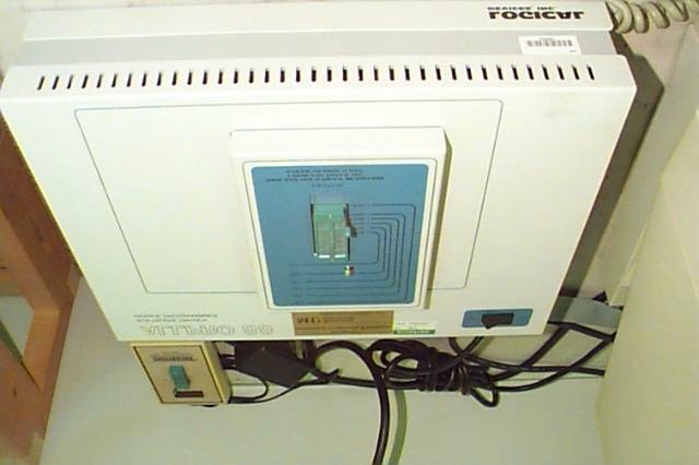
35 ChipMaster 6000 Intelligent Universal Programmer
36 Using the CM6000 Universal Programmer 1. Load the device 2. Select a device 3. Perform Blank Check 4. Erase device 5. Read jedec file 6. Program device 7. Verify

37 Insert Device into the socket 1. Make sure the busy light is off. 2. Lift the lever of the ZIF socket up. 3. Insert the device. Align the device with the bottom of the socket with pin 1 facing the top of the socket. 4. Press the lever of the ZIF socket down.
38 Startup

39 1. Type ALT-C or Select the Device Change Device menu item. 2. Select the device required: Use the mouse: Click on All, EPROM, PROM, PLD, or MPU Use the keyboard: Press TAB until the cursor is flashing in the Type box. Use the up and down arrows to go to the appropriate type. Press the space bar to select the type. 3. Enter the part number in the Search box. Use mouse: Click on Search Use keyboard: Press TAB until the cursor flashes in the Search box. Type in the part number. 4. Use the mouse to select a vendor. 5. Select a device and click OK. Use the TAB key to skip between various screens, use the arrow keys to move around each screen. Press <ENTER> to select the vendor/device. Select Device
40 Load File into Memory 1. Press ALT-L for Load File or select the File Load File menu item. 2. Press <TAB> to move the cursor to the list of files in the default directory 3. Select a file with the up and down arrow keys. 4. Press <ENTER>. 5. Select a file type with the up and down arrow keys. You want to select a jedec (.JED) file 6. Press <ENTER> to load the file.
")
41 Read Jedec (.JED) File
42 Program Device

43 Blank check the device Insert the device in the socket. 1. Select the device algorithm. 2. Press the ALT-B.
44 Erase the device This option is only available for devices that support chip erase. 1. Insert the device in the socket. 2. Select the device algorithm. 3. Press CTRL-F1 4. Click OK at the Are you sure you want to erase the device?
45 Program the device Before you program the device you have to load the file into memory. 1. Insert device into the socket. 2. Select the device algorithm. 3. Press ALT-P. or Click on the Prog. Button.
46 Verify the device 1. If the device is not inserted, insert it into the socket. 2. Select the device algorithm. The CM6000 verifies the device with the contents of the memory buffer. If the correct file is not loaded, load it now. 3. Press ALT-V. After programming, the CM6000 automatically verifies. You are done programming your chip.
47 AllPro 88 Programmer
48 Using the AllPro 88 Programmer Load Device into programmer Choose Library and Device from library Blank Check Device (optional) Read Jed file Program Device

49 Load Device in Programmer Place chip so Pin 1 faces front of programmer.

50 Choose Library and Device from library

51 Choose Library and Device from library

52 Choose Library

53 Choose Device

54 Blank Check Device (optional)
55 Read formatted File Select your.jed file from your floppy diskette
56 Program Device and you are done.
PALs, GALs & CUPL. What is Programmable Logic?
 PALs, GALs & CUPL A lesson on Programmable Logic Devices and programming them using CUPL What is Programmable Logic? Digital integrated circuits where the Boolean function can be determined by the user.
More Programming with CUPL
 More Programming with CUPL Compiling PLD File Use WinCUPL or use another text editor to create your file Save your file with the extension.pld Compile using WinCUPL make sure you have no errors. Save your.jed
Presentation 4: Programmable Combinational Devices
 Presentation 4: Programmable Combinational Devices Asst. Prof Dr. Ahmet ÖZKURT DEUEEE Based on the Presentation by Prof. Kim, Young Ho Dept. of Information Computer Engineering E-mail : yhkim@hyowon.cs.pusan.ac.kr
Lecture (09) Programmable Logic Devices programming using CUPL By: Dr. Ahmed ElShafee
 Programmable Logic Devices programming using CUPL By: Dr. Ahmed ElShafee") Lecture (09) Programmable Logic Devices programming using CUPL By: Dr. Ahmed ElShafee ١ Dr. Ahmed ElShafee, ACU : Spring 2018, CSE303 Logic design II What is Programmable Logic? Digital integrated circuits
Lecture (09) Programmable Logic Devices programming using CUPL By: Dr. Ahmed ElShafee ١ Dr. Ahmed ElShafee, ACU : Spring 2018, CSE303 Logic design II What is Programmable Logic? Digital integrated circuits
Programmable Logic Devices
 Programmable Logic Devices Programmable Logic Devices Fig. (1) General structure of PLDs Programmable Logic Device (PLD): is an integrated circuit with internal logic gates and/or connections that can
Code No: R Set No. 1
 Code No: R059210504 Set No. 1 II B.Tech I Semester Supplementary Examinations, February 2007 DIGITAL LOGIC DESIGN ( Common to Computer Science & Engineering, Information Technology and Computer Science
Unit 6 1.Random Access Memory (RAM) Chapter 3 Combinational Logic Design 2.Programmable Logic
 Chapter 3 Combinational Logic Design 2.Programmable Logic") EE 200: Digital Logic Circuit Design Dr Radwan E Abdel-Aal, COE Unit 6.Random Access Memory (RAM) Chapter 3 Combinational Logic Design 2. Logic Logic and Computer Design Fundamentals Part Implementation
EE 200: Digital Logic Circuit Design Dr Radwan E Abdel-Aal, COE Unit 6.Random Access Memory (RAM) Chapter 3 Combinational Logic Design 2. Logic Logic and Computer Design Fundamentals Part Implementation
MEMORY AND PROGRAMMABLE LOGIC
 MEMORY AND PROGRAMMABLE LOGIC Memory is a device where we can store and retrieve information It can execute a read and a write Programmable Logic is a device where we can store and retrieve information
Review: Chip Design Styles
 MPT-50 Introduction to omputer Design SFU, Harbour entre, Spring 007 Lecture 9: Feb. 6, 007 Programmable Logic Devices (PLDs) - Read Only Memory (ROM) - Programmable Array Logic (PAL) - Programmable Logic
Code No: R Set No. 1
 Code No: R059210504 Set No. 1 II B.Tech I Semester Regular Examinations, November 2007 DIGITAL LOGIC DESIGN ( Common to Computer Science & Engineering, Information Technology and Computer Science & Systems
Experiment 3: Logic Simplification
 Module: Logic Design Name:... University no:.. Group no:. Lab Partner Name: Mr. Mohamed El-Saied Experiment : Logic Simplification Objective: How to implement and verify the operation of the logical functions
PROGRAMMABLE LOGIC DEVICES
 PROGRAMMABLE LOGIC DEVICES Programmable logic devices (PLDs) are used for designing logic circuits. PLDs can be configured by the user to perform specific functions. The different types of PLDs available
Memory and Programmable Logic
 Memory and Programmable Logic Mano & Ciletti Chapter 7 By Suleyman TOSUN Ankara University Outline RAM Memory decoding Error detection and correction ROM Programmable Logic Array (PLA) Programmable Array
Embedded Controller Design. CompE 270 Digital Systems - 5. Objective. Application Specific Chips. User Programmable Logic. Copyright 1998 Ken Arnold 1
 CompE 270 Digital Systems - 5 Programmable Logic Ken Arnold Objective Application Specific ICs Introduce User Programmable Logic Common Architectures Programmable Array Logic Address Decoding Example Development
Memory and Programmable Logic
 Memory and Programmable Logic Memory units allow us to store and/or retrieve information Essentially look-up tables Good for storing data, not for function implementation Programmable logic device (PLD),
Programmable Logic Devices UNIT II DIGITAL SYSTEM DESIGN
 Programmable Logic Devices UNIT II DIGITAL SYSTEM DESIGN 2 3 4 5 6 7 8 9 2 3 4 5 6 7 8 9 2 Implementation in Sequential Logic 2 PAL Logic Implementation Design Example: BCD to Gray Code Converter A B
Code No: R Set No. 1
 Code No: R059210504 Set No. 1 II B.Tech I Semester Regular Examinations, November 2006 DIGITAL LOGIC DESIGN ( Common to Computer Science & Engineering, Information Technology and Computer Science & Systems
Chapter 13 Programmable Logic Device Architectures
 Chapter 13 Programmable Logic Device Architectures Chapter 13 Objectives Selected areas covered in this chapter: Describing different categories of digital system devices. Describing different types of
END-TERM EXAMINATION
 (Please Write your Exam Roll No. immediately) END-TERM EXAMINATION DECEMBER 2006 Exam. Roll No... Exam Series code: 100919DEC06200963 Paper Code: MCA-103 Subject: Digital Electronics Time: 3 Hours Maximum
Literal Cost F = BD + A B C + A C D F = BD + A B C + A BD + AB C F = (A + B)(A + D)(B + C + D )( B + C + D) L = 10
(A + D)(B + C + D )( B + C + D) L = 10") Circuit Optimization Goal: To obtain the simplest implementation for a given function Optimization is a more formal approach to simplification that is performed using a specific procedure or algorithm
Circuit Optimization Goal: To obtain the simplest implementation for a given function Optimization is a more formal approach to simplification that is performed using a specific procedure or algorithm
CPLD Software Tutorial FOR ALTERA MAX+PLUS II
 CPLD Software Tutorial FOR ALTERA MAX+PLUS II Note: This material was developed by William Kleitz for inclusion in his textbook Digital Electronics: A Practical Approach 6 th edition, (Prentice-Hall 2002).
Assignment (3-6) Boolean Algebra and Logic Simplification - General Questions
 Boolean Algebra and Logic Simplification - General Questions") Assignment (3-6) Boolean Algebra and Logic Simplification - General Questions 1. Convert the following SOP expression to an equivalent POS expression. 2. Determine the values of A, B, C, and D that make
Assignment (3-6) Boolean Algebra and Logic Simplification - General Questions 1. Convert the following SOP expression to an equivalent POS expression. 2. Determine the values of A, B, C, and D that make
Programmable Logic Devices (PLDs)
") Programmable Logic Devices (PLDs) 212: Digital Design I, week 13 PLDs basically store binary information in a volatile/nonvolatile device. Data is specified by designer and physically inserted (Programmed)
Programmable Logic Devices (PLDs) 212: Digital Design I, week 13 PLDs basically store binary information in a volatile/nonvolatile device. Data is specified by designer and physically inserted (Programmed)
R10. II B. Tech I Semester, Supplementary Examinations, May
 SET - 1 1. a) Convert the following decimal numbers into an equivalent binary numbers. i) 53.625 ii) 4097.188 iii) 167 iv) 0.4475 b) Add the following numbers using 2 s complement method. i) -48 and +31
Programmable Logic Devices. Programmable Read Only Memory (PROM) Example
 Example") Programmable Logic Devices Programmable Logic Devices (PLDs) are the integrated circuits. They contain an array of AND gates & another array of OR gates. There are three kinds of PLDs based on the type
Programmable Logic Devices Programmable Logic Devices (PLDs) are the integrated circuits. They contain an array of AND gates & another array of OR gates. There are three kinds of PLDs based on the type
Code No: 07A3EC03 Set No. 1
 Code No: 07A3EC03 Set No. 1 II B.Tech I Semester Regular Examinations, November 2008 SWITCHING THEORY AND LOGIC DESIGN ( Common to Electrical & Electronic Engineering, Electronics & Instrumentation Engineering,
Introduction to Programmable Logic Devices (Class 7.2 2/28/2013)
") Introduction to Programmable Logic Devices (Class 7.2 2/28/2013) CSE 2441 Introduction to Digital Logic Spring 2013 Instructor Bill Carroll, Professor of CSE Today s Topics Complexity issues Implementation
Introduction to Programmable Logic Devices (Class 7.2 2/28/2013) CSE 2441 Introduction to Digital Logic Spring 2013 Instructor Bill Carroll, Professor of CSE Today s Topics Complexity issues Implementation
BHARATHIDASAN ENGINEERING COLLEGE Degree / Branch : B.E./ECE Year / Sem : II/ III Sub.Code / Name : EC6302/DIGITAL ELECTRONICS
 BHARATHIDASAN ENGINEERING COLLEGE Degree / Branch : B.E./ECE Year / Sem : II/ III Sub.Code / Name : EC6302/DIGITAL ELECTRONICS FREQUENTLY ASKED QUESTIONS UNIT I MINIMIZATION TECHNIQUES AND LOGIC GATES
LSN 6 Programmable Logic Devices
 LSN 6 Programmable Logic Devices Department of Engineering Technology LSN 6 What Are PLDs? Functionless devices in base form Require programming to operate The logic function of the device is programmed
VALLIAMMAI ENGINEERING COLLEGE. SRM Nagar, Kattankulathur DEPARTMENT OF ELECTRONICS AND COMMUNICATION ENGINEERING EC6302 DIGITAL ELECTRONICS
 VALLIAMMAI ENGINEERING COLLEGE SRM Nagar, Kattankulathur-603 203 DEPARTMENT OF ELECTRONICS AND COMMUNICATION ENGINEERING EC6302 DIGITAL ELECTRONICS YEAR / SEMESTER: II / III ACADEMIC YEAR: 2015-2016 (ODD
QUESTION BANK FOR TEST
 CSCI 2121 Computer Organization and Assembly Language PRACTICE QUESTION BANK FOR TEST 1 Note: This represents a sample set. Please study all the topics from the lecture notes. Question 1. Multiple Choice
DIGITAL SYSTEM FUNDAMENTALS (ECE421) DIGITAL ELECTRONICS FUNDAMENTAL (ECE4220. PROGRAMMABLE LOGIC DEVICES (PLDs)
 DIGITAL ELECTRONICS FUNDAMENTAL (ECE4220. PROGRAMMABLE LOGIC DEVICES (PLDs)") COURSE / CODE DIGITAL SYSTEM FUNDAMENTALS (ECE421) DIGITAL ELECTRONICS FUNDAMENTAL (ECE4220 PROGRAMMABLE LOGIC DEVICES (PLDs) A PLD, or programmable logic device, is an electronic component that is used
COURSE / CODE DIGITAL SYSTEM FUNDAMENTALS (ECE421) DIGITAL ELECTRONICS FUNDAMENTAL (ECE4220 PROGRAMMABLE LOGIC DEVICES (PLDs) A PLD, or programmable logic device, is an electronic component that is used
Purdue IMPACT 2015 Edition by D. G. Meyer. Introduction to Digital System Design. Module 2 Combinational Logic Circuits
 Purdue IMPACT 25 Edition by D. G. Meyer Introduction to Digital System Design Module 2 Combinational Logic Circuits Glossary of Common Terms DISCRETE LOGIC a circuit constructed using small-scale integrated
Using Programmable Logic and the PALCE22V10
 Using Programmable Logic and the PALCE22V10 Programmable logic chips (like the PALCE22V10) provide a convenient solution for glue logic and state machine control required by your design. A single PAL chip
CHAPTER 9 MULTIPLEXERS, DECODERS, AND PROGRAMMABLE LOGIC DEVICES
 CHAPTER 9 MULTIPLEXERS, DECODERS, AND PROGRAMMABLE LOGIC DEVICES This chapter in the book includes: Objectives Study Guide 9.1 Introduction 9.2 Multiplexers 9.3 Three-State Buffers 9.4 Decoders and Encoders
B.Tech II Year I Semester (R13) Regular Examinations December 2014 DIGITAL LOGIC DESIGN
 Regular Examinations December 2014 DIGITAL LOGIC DESIGN") B.Tech II Year I Semester () Regular Examinations December 2014 (Common to IT and CSE) (a) If 1010 2 + 10 2 = X 10, then X is ----- Write the first 9 decimal digits in base 3. (c) What is meant by don
B.Tech II Year I Semester () Regular Examinations December 2014 (Common to IT and CSE) (a) If 1010 2 + 10 2 = X 10, then X is ----- Write the first 9 decimal digits in base 3. (c) What is meant by don
Semiconductor Memories: RAMs and ROMs
 Semiconductor Memories: RAMs and ROMs Lesson Objectives: In this lesson you will be introduced to: Different memory devices like, RAM, ROM, PROM, EPROM, EEPROM, etc. Different terms like: read, write,
Fig. 6-1 Conventional and Array Logic Symbols for OR Gate
 6- (a) Conventional symbol (b) Array logic symbol Fig. 6- Conventional and Array Logic Symbols for OR Gate 2 Prentice Hall, Inc. 6-2 k address lines Read n data input lines emory unit 2 k words n bits
R07
 www..com www..com SET - 1 II B. Tech I Semester Supplementary Examinations May 2013 SWITCHING THEORY AND LOGIC DESIGN (Com. to EEE, EIE, BME, ECC) Time: 3 hours Max. Marks: 80 Answer any FIVE Questions
Evolution of Implementation Technologies. ECE 4211/5211 Rapid Prototyping with FPGAs. Gate Array Technology (IBM s) Programmable Logic
 Programmable Logic") ECE 42/52 Rapid Prototyping with FPGAs Dr. Charlie Wang Department of Electrical and Computer Engineering University of Colorado at Colorado Springs Evolution of Implementation Technologies Discrete devices:
ECE 42/52 Rapid Prototyping with FPGAs Dr. Charlie Wang Department of Electrical and Computer Engineering University of Colorado at Colorado Springs Evolution of Implementation Technologies Discrete devices:
SHRI ANGALAMMAN COLLEGE OF ENGINEERING. (An ISO 9001:2008 Certified Institution) SIRUGANOOR, TIRUCHIRAPPALLI
 SIRUGANOOR, TIRUCHIRAPPALLI") SHRI ANGALAMMAN COLLEGE OF ENGINEERING AND TECHNOLOGY (An ISO 9001:2008 Certified Institution) SIRUGANOOR, TIRUCHIRAPPALLI 621 105 DEPARTMENT OF ELECTRONICS AND COMMUNICATION ENGINEERING EC1201 DIGITAL
SHRI ANGALAMMAN COLLEGE OF ENGINEERING AND TECHNOLOGY (An ISO 9001:2008 Certified Institution) SIRUGANOOR, TIRUCHIRAPPALLI 621 105 DEPARTMENT OF ELECTRONICS AND COMMUNICATION ENGINEERING EC1201 DIGITAL
VALLIAMMAI ENGINEERING COLLEGE
 VALLIAMMAI ENGINEERING COLLEGE SRM Nagar, Kattankulathur 603 203 DEPARTMENT OF INFORMATION TECHNOLOGY QUESTION BANK Academic Year 2018 19 III SEMESTER CS8351-DIGITAL PRINCIPLES AND SYSTEM DESIGN Regulation
VALLIAMMAI ENGINEERING COLLEGE
 VALLIAMMAI ENGINEERING COLLEGE SRM Nagar, Kattankulathur 603 203 DEPARTMENT OF INFORMATION TECHNOLOGY & COMPUTER SCIENCE AND ENGINEERING QUESTION BANK II SEMESTER CS6201- DIGITAL PRINCIPLE AND SYSTEM DESIGN
Question No: 1 ( Marks: 1 ) - Please choose one A SOP expression is equal to 1
 - Please choose one A SOP expression is equal to 1") ASSALAM O ALAIKUM all fellows ALL IN ONE Mega File CS302 Midterm PAPERS, MCQz & subjective Created BY Farhan& Ali BS (cs) 3rd sem Hackers Group Mandi Bahauddin Remember us in your prayers Mindhacker124@gmail.com
ASSALAM O ALAIKUM all fellows ALL IN ONE Mega File CS302 Midterm PAPERS, MCQz & subjective Created BY Farhan& Ali BS (cs) 3rd sem Hackers Group Mandi Bahauddin Remember us in your prayers Mindhacker124@gmail.com
Gate Level Minimization Map Method
 Gate Level Minimization Map Method Complexity of hardware implementation is directly related to the complexity of the algebraic expression Truth table representation of a function is unique Algebraically
 www.vidyarthiplus.com Question Paper Code : 31298 B.E./B.Tech. DEGREE EXAMINATION, NOVEMBER/DECEMBER 2013. Third Semester Computer Science and Engineering CS 2202/CS 34/EC 1206 A/10144 CS 303/080230012--DIGITAL
Memory and Programmable Logic
 Digital Circuit Design and Language Memory and Programmable Logic Chang, Ik Joon Kyunghee University Memory Classification based on functionality ROM : Read-Only Memory RWM : Read-Write Memory RWM NVRWM
Digital Systems Design with PLDs and FPGAs Kuruvilla Varghese Department of Electronic Systems Engineering Indian Institute of Science Bangalore
 Digital Systems Design with PLDs and FPGAs Kuruvilla Varghese Department of Electronic Systems Engineering Indian Institute of Science Bangalore Lecture-32 Simple PLDs So welcome to just lecture on programmable
COLLEGE OF ENGINEERING DEPARTMENT OF ELECTRICAL AND ELECTRONICS ENGINEERING QUESTION BANK SUBJECT CODE & NAME: EC 1312 DIGITAL LOGIC CIRCUITS UNIT I
 KINGS COLLEGE OF ENGINEERING DEPARTMENT OF ELECTRICAL AND ELECTRONICS ENGINEERING QUESTION BANK SUBJECT CODE & NAME: EC 1312 DIGITAL LOGIC CIRCUITS YEAR / SEM: III / V UNIT I NUMBER SYSTEM & BOOLEAN ALGEBRA
ENGINEERS ACADEMY. 7. Given Boolean theorem. (a) A B A C B C A B A C. (b) AB AC BC AB BC. (c) AB AC BC A B A C B C.
 A B A C B C A B A C. (b) AB AC BC AB BC. (c) AB AC BC A B A C B C.") Digital Electronics Boolean Function QUESTION BANK. The Boolean equation Y = C + C + C can be simplified to (a) (c) A (B + C) (b) AC (d) C. The Boolean equation Y = (A + B) (A + B) can be simplified to
Digital Electronics Boolean Function QUESTION BANK. The Boolean equation Y = C + C + C can be simplified to (a) (c) A (B + C) (b) AC (d) C. The Boolean equation Y = (A + B) (A + B) can be simplified to
Injntu.com Injntu.com Injntu.com R16
 1. a) What are the three methods of obtaining the 2 s complement of a given binary (3M) number? b) What do you mean by K-map? Name it advantages and disadvantages. (3M) c) Distinguish between a half-adder
Gate-Level Minimization
 MEC520 디지털공학 Gate-Level Minimization Jee-Hwan Ryu School of Mechanical Engineering Gate-Level Minimization-The Map Method Truth table is unique Many different algebraic expression Boolean expressions may
DHANALAKSHMI SRINIVASAN COLLEGE OF ENGINEERING AND TECHNOLOGY
 DHANALAKSHMI SRINIVASAN COLLEGE OF ENGINEERING AND TECHNOLOGY Dept/Sem: II CSE/03 DEPARTMENT OF ECE CS8351 DIGITAL PRINCIPLES AND SYSTEM DESIGN UNIT I BOOLEAN ALGEBRA AND LOGIC GATES PART A 1. How many
CSCI 220: Computer Architecture I Instructor: Pranava K. Jha. Simplification of Boolean Functions using a Karnaugh Map
 CSCI 22: Computer Architecture I Instructor: Pranava K. Jha Simplification of Boolean Functions using a Karnaugh Map Q.. Plot the following Boolean function on a Karnaugh map: f(a, b, c, d) = m(, 2, 4,
PLAs & PALs. Programmable Logic Devices (PLDs) PLAs and PALs
 PLAs and PALs") PLAs & PALs Programmable Logic Devices (PLDs) PLAs and PALs PLAs&PALs By the late 1970s, standard logic devices were all the rage, and printed circuit boards were loaded with them. To offer the ultimate
PLAs & PALs Programmable Logic Devices (PLDs) PLAs and PALs PLAs&PALs By the late 1970s, standard logic devices were all the rage, and printed circuit boards were loaded with them. To offer the ultimate
Ryerson Polytechnic University Department of Electrical and Computer Engineering ELE 328 Digital Systems and Microprocessors
 Ryerson Polytechnic University Department of Electrical and Computer Engineering ELE 328 Digital Systems and Microprocessors Lab 1 CAD Tools 10 marks (2 Weeks) Fall 2002 Due Date: Week 4 Part A PALASM
DIGITAL CIRCUIT LOGIC UNIT 9: MULTIPLEXERS, DECODERS, AND PROGRAMMABLE LOGIC DEVICES
 DIGITAL CIRCUIT LOGIC UNIT 9: MULTIPLEXERS, DECODERS, AND PROGRAMMABLE LOGIC DEVICES 1 Learning Objectives 1. Explain the function of a multiplexer. Implement a multiplexer using gates. 2. Explain the
Introduction to GAL Device Architectures
 ntroduction to GAL evice Architectures Overview n 195, Lattice Semiconductor introduced a new type of programmable logic device (PL) that transformed the PL market: the Generic Array Logic (GAL) device.
HANSABA COLLEGE OF ENGINEERING & TECHNOLOGY (098) SUBJECT: DIGITAL ELECTRONICS ( ) Assignment
 SUBJECT: DIGITAL ELECTRONICS ( ) Assignment") Assignment 1. What is multiplexer? With logic circuit and function table explain the working of 4 to 1 line multiplexer. 2. Implement following Boolean function using 8: 1 multiplexer. F(A,B,C,D) = (2,3,5,7,8,9,12,13,14,15)
Assignment 1. What is multiplexer? With logic circuit and function table explain the working of 4 to 1 line multiplexer. 2. Implement following Boolean function using 8: 1 multiplexer. F(A,B,C,D) = (2,3,5,7,8,9,12,13,14,15)
2008 The McGraw-Hill Companies, Inc. All rights reserved.
 28 The McGraw-Hill Companies, Inc. All rights reserved. 28 The McGraw-Hill Companies, Inc. All rights reserved. All or Nothing Gate Boolean Expression: A B = Y Truth Table (ee next slide) or AB = Y 28
PEEL 16V8-15/-25 CMOS Programmable Electrically Erasable Logic
 -5/-25 CMOS Programmable Electrically Erasable Logic Compatible with Popular 6V8 Devices 6V8 socket and function compatible Programs with standard 6V8 JEDEC file 20-pin DP and PLCC packages CMOS Electrically
Chapter 2 Combinational Logic Circuits
 Logic and Computer Design Fundamentals Chapter 2 Combinational Logic Circuits Part 2 Circuit Optimization Overview Part Gate Circuits and Boolean Equations Binary Logic and Gates Boolean Algebra Standard
Date Performed: Marks Obtained: /10. Group Members (ID):. Experiment # 04. Boolean Expression Simplification and Implementation
:. Experiment # 04. Boolean Expression Simplification and Implementation") Name: Instructor: Engr. Date Performed: Marks Obtained: /10 Group Members (ID):. Checked By: Date: Experiment # 04 Boolean Expression Simplification and Implementation OBJECTIVES: To understand the utilization
Name: Instructor: Engr. Date Performed: Marks Obtained: /10 Group Members (ID):. Checked By: Date: Experiment # 04 Boolean Expression Simplification and Implementation OBJECTIVES: To understand the utilization
APPENDIX A SHORT QUESTIONS AND ANSWERS
 APPENDIX A SHORT QUESTIONS AND ANSWERS Unit I Boolean Algebra and Logic Gates Part - A 1. Define binary logic? Binary logic consists of binary variables and logical operations. The variables are designated
Combinational Digital Design. Laboratory Manual. Experiment #3. Boolean Algebra Continued
 The Islamic University of Gaza Engineering Faculty Department of Computer Engineering Fall 2017 ECOM 2013 Khaleel I. Shaheen Combinational Digital Design Laboratory Manual Experiment #3 Boolean Algebra
CONTENTS CHAPTER 1: NUMBER SYSTEM. Foreword...(vii) Preface... (ix) Acknowledgement... (xi) About the Author...(xxiii)
 Preface... (ix) Acknowledgement... (xi) About the Author...(xxiii)") CONTENTS Foreword...(vii) Preface... (ix) Acknowledgement... (xi) About the Author...(xxiii) CHAPTER 1: NUMBER SYSTEM 1.1 Digital Electronics... 1 1.1.1 Introduction... 1 1.1.2 Advantages of Digital Systems...
CONTENTS Foreword...(vii) Preface... (ix) Acknowledgement... (xi) About the Author...(xxiii) CHAPTER 1: NUMBER SYSTEM 1.1 Digital Electronics... 1 1.1.1 Introduction... 1 1.1.2 Advantages of Digital Systems...
Chapter 6 Selected Design Topics
 Logic and Computer Design Fundamentals Chapter 6 Selected Design Topics Part 4 Programmable Implementation Technologies Charles Kime & Thomas Kaminski 2008 Pearson Education, Inc. (Hyperlinks are active
2.1 Binary Logic and Gates
 1 EED2003 Digital Design Presentation 2: Boolean Algebra Asst. Prof.Dr. Ahmet ÖZKURT Asst. Prof.Dr Hakkı T. YALAZAN Based on the Lecture Notes by Jaeyoung Choi choi@comp.ssu.ac.kr Fall 2000 2.1 Binary
UNIT V (PROGRAMMABLE LOGIC DEVICES)
") UNIT V (PROGRAMMABLE LOGIC DEVICES) Introduction There are two types of memories that are used in digital systems: Random-access memory(ram): perform both the write and read operations. Read-only memory(rom):
UNIT V (PROGRAMMABLE LOGIC DEVICES) Introduction There are two types of memories that are used in digital systems: Random-access memory(ram): perform both the write and read operations. Read-only memory(rom):
FYSE420 DIGITAL ELECTRONICS. Lecture 7
 FYSE420 DIGITAL ELECTRONICS Lecture 7 1 [1] [2] [3] DIGITAL LOGIC CIRCUIT ANALYSIS & DESIGN Nelson, Nagle, Irvin, Carrol ISBN 0-13-463894-8 DIGITAL DESIGN Morris Mano Fourth edition ISBN 0-13-198924-3
Chapter 2 Combinational
 Computer Engineering 1 (ECE290) Chapter 2 Combinational Logic Circuits Part 2 Circuit Optimization HOANG Trang 2008 Pearson Education, Inc. Overview Part 1 Gate Circuits and Boolean Equations Binary Logic
Lecture 4: Implementation AND, OR, NOT Gates and Complement
 EE210: Switching Systems Lecture 4: Implementation AND, OR, NOT Gates and Complement Prof. YingLi Tian Feb. 13, 2018 Department of Electrical Engineering The City College of New York The City University
Ch. 5 : Boolean Algebra &
 Ch. 5 : Boolean Algebra & Reduction elektronik@fisika.ui.ac.id Objectives Should able to: Write Boolean equations for combinational logic applications. Utilize Boolean algebra laws and rules for simplifying
SIR C.R.REDDY COLLEGE OF ENGINEERING, ELURU DEPARTMENT OF INFORMATION TECHNOLOGY LESSON PLAN
 SIR C.R.REDDY COLLEGE OF ENGINEERING, ELURU DEPARTMENT OF INFORMATION TECHNOLOGY LESSON PLAN SUBJECT: CSE 2.1.6 DIGITAL LOGIC DESIGN CLASS: 2/4 B.Tech., I SEMESTER, A.Y.2017-18 INSTRUCTOR: Sri A.M.K.KANNA
PEEL 18CV8-5/-7/-10/-15/-25 CMOS Programmable Electrically Erasable Logic Device Features
 PEEL 18CV8-5/-7/-10/-15/-25 CMOS Programmable Electrically Erasable Logic Device Features Multiple Speed Power, Temperature Options - VCC = 5 Volts ±10% - Speeds ranging from 5ns to 25 ns - Power as low
R.M.D. ENGINEERING COLLEGE R.S.M. Nagar, Kavaraipettai
 L T P C R.M.D. ENGINEERING COLLEGE R.S.M. Nagar, Kavaraipettai- 601206 DEPARTMENT OF ELECTRONICS AND COMMUNICATION ENGINEERING EC8392 UNIT - I 3 0 0 3 OBJECTIVES: To present the Digital fundamentals, Boolean
SIDDHARTH GROUP OF INSTITUTIONS :: PUTTUR Siddharth Nagar, Narayanavanam Road QUESTION BANK (DESCRIPTIVE)
") SIDDHARTH GROUP OF INSTITUTIONS :: PUTTUR Siddharth Nagar, Narayanavanam Road 517583 QUESTION BANK (DESCRIPTIVE) Subject with Code : STLD(16EC402) Year & Sem: II-B.Tech & I-Sem Course & Branch: B.Tech
SIDDHARTH GROUP OF INSTITUTIONS :: PUTTUR Siddharth Nagar, Narayanavanam Road 517583 QUESTION BANK (DESCRIPTIVE) Subject with Code : STLD(16EC402) Year & Sem: II-B.Tech & I-Sem Course & Branch: B.Tech
Chapter 3. Gate-Level Minimization. Outlines
 Chapter 3 Gate-Level Minimization Introduction The Map Method Four-Variable Map Five-Variable Map Outlines Product of Sums Simplification Don t-care Conditions NAND and NOR Implementation Other Two-Level
Programmable Logic Devices. PAL & Jedec Programming
 Programmable Logic Devices PAL & Jedec Programming PAL Devices: PAL = Programmable Array Logic The PAL naming is trademark of the AMD Firm, but Lattice also use these circuits. The PAL device is a PLD
Philadelphia University Student Name: Student Number:
 Philadelphia University Student Name: Student Number: Faculty of Engineering Serial Number: Final Exam, First Semester: 2018/2019 Dept. of Computer Engineering Course Title: Logic Circuits Date: 03/01/2019
Hours / 100 Marks Seat No.
 17333 13141 3 Hours / 100 Seat No. Instructions (1) All Questions are Compulsory. (2) Answer each next main Question on a new page. (3) Illustrate your answers with neat sketches wherever necessary. (4)
Combinational Logic Use the Boolean Algebra and the minimization techniques to design useful circuits No feedback, no memory Just n inputs, m outputs
 Combinational Logic Use the Boolean Algebra and the minimization techniques to design useful circuits No feedback, no memory Just n inputs, m outputs and an arbitrary truth table Analysis Procedure We
PEEL 20V8-15/-25 CMOS Programmable Electrically Erasable Logic Device
 Preliminary Commercial -15/-25 CMOS Programmable Electrically Erasable Logic Device Compatible with Popular 20V8 Devices 20V8 socket and function compatible Programs with standard 20V8 JEDEC file 24-pin
MULTIMEDIA COLLEGE JALAN GURNEY KIRI KUALA LUMPUR
 STUDENT IDENTIFICATION NO MULTIMEDIA COLLEGE JALAN GURNEY KIRI 54100 KUALA LUMPUR SECOND SEMESTER FINAL EXAMINATION, 2013/2014 SESSION ITC2223 COMPUTER ORGANIZATION & ARCHITECTURE DSEW-E-F 1/13 18 FEBRUARY
Copyright 2011 R.S.R. Electronics, Inc. All rights reserved. 04/11. Ver. 1.0web
 For XILINX WebPack Copyright 2011 R.S.R. Electronics, Inc. All rights reserved. 04/11 Ver. 1.0web 1 Table of Contents 1.0 INTRODUCTION...3 2.0 GENERAL DESCRIPTION...5 3.0 BRIEF DESCRIPTION Of PLDT-3 BOARD...6
ELCT201: DIGITAL LOGIC DESIGN
 ELCT201: DIGITAL LOGIC DESIGN Dr. Eng. Haitham Omran, haitham.omran@guc.edu.eg Dr. Eng. Wassim Alexan, wassim.joseph@guc.edu.eg Lecture 3 Following the slides of Dr. Ahmed H. Madian محرم 1439 ه Winter
EE4380 Microprocessor Design Project
 EE4380 Microprocessor Design Project Fall 2002 Class 1 Pari vallal Kannan Center for Integrated Circuits and Systems University of Texas at Dallas Introduction What is a Microcontroller? Microcontroller
UNIT - V MEMORY P.VIDYA SAGAR ( ASSOCIATE PROFESSOR) Department of Electronics and Communication Engineering, VBIT
 Department of Electronics and Communication Engineering, VBIT") UNIT - V MEMORY P.VIDYA SAGAR ( ASSOCIATE PROFESSOR) contents Memory: Introduction, Random-Access memory, Memory decoding, ROM, Programmable Logic Array, Programmable Array Logic, Sequential programmable
UNIT - V MEMORY P.VIDYA SAGAR ( ASSOCIATE PROFESSOR) contents Memory: Introduction, Random-Access memory, Memory decoding, ROM, Programmable Logic Array, Programmable Array Logic, Sequential programmable
Simplification of Boolean Functions
 COM111 Introduction to Computer Engineering (Fall 2006-2007) NOTES 5 -- page 1 of 5 Introduction Simplification of Boolean Functions You already know one method for simplifying Boolean expressions: Boolean
ELCT201: DIGITAL LOGIC DESIGN
 ELCT201: DIGITAL LOGIC DESIGN Dr. Eng. Haitham Omran, haitham.omran@guc.edu.eg Dr. Eng. Wassim Alexan, wassim.joseph@guc.edu.eg Lecture 3 Following the slides of Dr. Ahmed H. Madian ذو الحجة 1438 ه Winter
Lecture 13: Memory and Programmable Logic
 Lecture 13: Memory and Programmable Logic Syed M. Mahmud, Ph.D ECE Department Wayne State University Aby K George, ECE Department, Wayne State University Contents Introduction Random Access Memory Memory
(ii) Simplify and implement the following SOP function using NOR gates:
 Simplify and implement the following SOP function using NOR gates:") DHANALAKSHMI COLLEGE OF ENGINEERING DEPARTMENT OF ELECTRONICS AND COMMUNICATION ENGINEERING EE6301 DIGITAL LOGIC CIRCUITS UNIT I NUMBER SYSTEMS AND DIGITAL LOGIC FAMILIES PART A 1. How can an OR gate be
DHANALAKSHMI COLLEGE OF ENGINEERING DEPARTMENT OF ELECTRONICS AND COMMUNICATION ENGINEERING EE6301 DIGITAL LOGIC CIRCUITS UNIT I NUMBER SYSTEMS AND DIGITAL LOGIC FAMILIES PART A 1. How can an OR gate be
Programmable Logic Devices
 Programmable Logic Devices INTRODUCTION A programmable logic device or PLD is an electronic component used to build reconfigurable digital circuits. Unlike a logic gate, which has a fixed function, a PLD
Programmable Logic. Module: EE2C2 Digital Design. Lecturer: James Grimbleby. j.b.grimbleby reading.ac.uk. Number of Lectures: 6
 Programmable Logic Module: EE2C2 Digital Design Lecturer: URL: http://www.personal.rdg.ac.uk/~stsgrimb/ personal rdg ac stsgrimb/ email: j.b.grimbleby reading.ac.uk Number of Lectures: 6 Recommended course
DKT 122/3 DIGITAL SYSTEM 1
 Company LOGO DKT 122/3 DIGITAL SYSTEM 1 BOOLEAN ALGEBRA (PART 2) Boolean Algebra Contents Boolean Operations & Expression Laws & Rules of Boolean algebra DeMorgan s Theorems Boolean analysis of logic circuits
Principles of Digital Techniques PDT (17320) Assignment No State advantages of digital system over analog system.
 Assignment No State advantages of digital system over analog system.") Assignment No. 1 1. State advantages of digital system over analog system. 2. Convert following numbers a. (138.56) 10 = (?) 2 = (?) 8 = (?) 16 b. (1110011.011) 2 = (?) 10 = (?) 8 = (?) 16 c. (3004.06)
Assignment No. 1 1. State advantages of digital system over analog system. 2. Convert following numbers a. (138.56) 10 = (?) 2 = (?) 8 = (?) 16 b. (1110011.011) 2 = (?) 10 = (?) 8 = (?) 16 c. (3004.06)
ECE/Comp Sci 352 Digital Systems Fundamentals Kewal K. Saluja and Yu Hen Hu Spring Logic and Computer Design Fundamentals.
 University of Wisconsin - Madison ECE/Comp Sci 352 Digital Systems Fundamentals Kewal K. Saluja and Yu Hen Hu Spring 2002 Chapter 6 Part 2 Memories & Programmable Logic Devices Originals by: Charles R.
Announcements. Chapter 2 - Part 1 1
 Announcements If you haven t shown the grader your proof of prerequisite, please do so by 11:59 pm on 09/05/2018 (Wednesday). I will drop students that do not show us the prerequisite proof after this
User's Guide COPYRIGHTS. For Windows 95/98/NT/2000. SUPERPRO Series Universal Programmers
 SUPERPRO Series Universal Programmers For Windows 95/98/NT/2000 User's Guide COPYRIGHTS Software Copyrights User's Guide Copyrights 1997-2006 XELTEK 1997-2006 XELTEK This software product is copyrighted.
Digital Systems Design with PLDs and FPGAs Kuruvilla Varghese Department of Electronic Systems Engineering Indian Institute of Science Bangalore
 Digital Systems Design with PLDs and FPGAs Kuruvilla Varghese Department of Electronic Systems Engineering Indian Institute of Science Bangalore Lecture-31 Evolution of PLDs So welcome to this lecture