User Manual for HMX1-AS2
|
|
|
- Jennifer Carson
- 6 years ago
- Views:
Transcription


1 User Manual for HMX1-AS2
2 Disclaimer. The information in this document is provided in connection with Gleichmann Electronics Research (GE Research) products. GE Research makes no representations or warranties with respect to the accuracy or completeness of the document and reserves the right to make changes to specification and product description at any time without notice. GE Research does not accept any liability to the accuracy of the design completed by the developer, whether original design, copied from schematics and/or application notes, supplied by GE Research and/or otherwise. The final circuit integrity and testing is solely the responsibility of the design authority. GE Research accept no responsibility and/or liability. HMX1-AS2 manual Martina Zeinzinger Version: Copyright Notice This document is copyrighted, 2008, by Gleichmann Electronics Research (Austria) GmbH & Co KG. All rights are reserved. Gleichmann Electronics Research (Austria) GmbH & Co KG reserves the right to make improvements to the products described in this manual at any time without notice. No part of this manual may be reproduced, copied, translated or transmitted in any form or by any means without the prior written permission of Gleichmann Electronics Research (Austria) GmbH & Co KG. Information provided in this manual is intended to be accurate and reliable. However, Gleichmann Electronics Research (Austria) GmbH & Co KG assumes no responsibility for its use, nor for any infringements upon the rights of third parties which may result from its use. 2
3 CONTENTS Contents Contents 3 1 Introduction System Overview General Information Reset LEDs AES Clock Factory Clock Distribution Configuration via Flash Fan Control CPLD for USB Blaster and FCP FCP JTAG configuration Connection to the CPLD for Clock Factory and Configuration Elastomer Connectors Module Connectors JTAG Global Reset Clocks Power Control I/Os for Peripherals Hpe Childboard Connectors Hpe Childboard Hpe Childboard Power Supply Power Source Generated Power I/O Power DUT-FPGA PLLs Connection to the CPLD for Clock Factory and Configuration Configuration Pins for the DUT-FPGA#1 by the CPLD for Clock Factory and Configuration Clocks I/O Pins: Negative Clock Inputs
4 CONTENTS Fast PLL Clock Inputs PLL Output Clocks Other I/O pins Connection to the CPLD for USB Blaster and FCP Dedicated Pins on the DUT-FPGA# Thermal Control JTAG Pins Configuration Pins Other dedicated Configuration Pins JTAG Pins for internal JTAG Core Clock from Oscillator Hpe Childboard Differential Receive Channels Transmit Channels Configuration Pins for the DUT-FPGA#1 by the Hpe Childboard Other pins Hpe Childboard Connector to the Mainboard Hpe Childboard Hpe Childboard Audio Interface (AC97) A/D Converter (ADC) and D/A Converter (DAC) CAN Interface External User Interface Ethernet Interface Expansion Connector Parallel Flash Human Interface I 2 C LCD Connector LIN Interface Memory PS/2 Ports Serial Interface (RS232) SD Card Reader Asynchronous SRAM x 4 Key Matrix USB Target Connector USB Host and On The Go (OTG) Connector VGA Interface System Reset Powerl Reset Specifications HMX1-AS2 Board HMX1-AS2 in the case
5 CONTENTS 9 Trouble Shooting Testing the hardware Generell Information Software which is recommended for testing Testroutine started automatically Starting the testroutine over Ethernet Index 56 5
6 6 CONTENTS
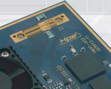
7 1 Introduction Attention The HMX1-AS2 is a FPGA development system therefore it is not designed for a worst case scenario. If it is used with very high performance, it is possible that the FGPA is not cooled sufficiently and/or the case overheats. It is the user s responsibility to proof the feasibility of the FPGA-design. In case of overheating, the clocks comming from the Clock Factory switchs off. If this protection mechanism is evaded, the consequence is the expiration of any guarantee. The name HMX1-AS2 stands for Hpe Module X1 stuffed with an Altera Stratix II FPGA. HMX1-AS2-60 means that the FPGA EP2S60F1020C3N is stuffed, HMX1-AS2-90 means that the FPGA EP2S90F1020C3N is stuffed and HMX1-AS2-180 means that the FPGA EP2S180F1020C3N is stuffed. The HMX1-AS2 is designed to be used in conjunction with the mainboard Hpe midi. The module is compatible to the former FPGA modules from Gleichmann Electronics Reseach, however, the mechanical outlines are different. A Altera Stratix II device is the main part of this module which can be used for the functional verification of high complex digital circuits and for SEmulation. The connection to the mainboard is done by two elastomer module connectors. 1.1 System Overview The following features are the most important parts of this FPGA module: one 1020 pin Altera Stratix II FPGA EP2S60F1020C3N, EP2S90F1020C3N or EP2S180F1020C3N (DUT-FPGA#1) two 364 pin elastomer module connectors (X1, X2) two 132 pin elastomer Hpe childboard connectors (X3, X4), one with low voltage differential signals (LVDS) flash for the configuration of the FPGA CPLD for clock distribution (clock factory), configuration and fan control CPLD for FPGA Code Protection (FCP) and Altera USB blaster The FPGA on the HMX1-AS2 is the fastest one of its family and it is used in a 1020-pin package. Beside that, it is possible to choose between three differnt sizes of the FPGA. The EP2S180F1020C3N offers three times the size of the EP2S60F1020C3N. The naming convention of this manual is based on the assumption that the HMX1-AS2 is used together with the Hpe midi and the Hpe childboard HC-PCIe in the SEmulator mode. The HC-PCIe has to be stucked on the Hpe childboard connector X3 and mainly consits of of an FPGA the Communication Controller which handles the connection to the PC via PCI Express. Figure 1.1 gives you a graphical overview of the components on the HMX1-AS2. 7

8 1 Introduction Figure 1.1: The HMX1-AS2 Block Diagram 8
9 2 General Information 2.1 Reset There is one system wide reset (PWR RESET#) which resets all CPLDs and the FPGA on the HMX1-AS LEDs Looking at the front side of your HMX1-AS2 you find nine LEDs. If the HMX1-AS2 is in the case together with a mainboard, you find the LEDs on the front side in the upper row (refer to figure 2.1). The first two LEDs from the right side are yellow and in a box named Fan. The right LED shows the activity of of the fan for the Communication Controller on the HC-PCIe. The LED on the left shows the fan activity for the DUT-FPGA#1. The next two LEDs are green and in a box named Power. The right one shows power good for 2.5 V and the left one signals power good for 1.2 V. The next three LEDs are in a box named ComCon and have a blue colour. These LEDs can only be lit when the HC-PCIe is connected. The left one stands for data transfer (DT), the one in the middle signals connection to the PC via PCI Express (PC) and the left one shows that the Communication Controller is ready (CC). The two blue LEDs on the left side are named Config Done. The right one shows that the Clock Factory (CF) is prepared and the left one signals that the DUT-FPGA#1 is configured. 2.3 AES AES is a block cipher standard. The DUT-FPGA#1 can be protected with AES. The key for AES can only be programmed once to each FPGA. That is to say, when the key is programmed, it can be neither changed nor deleted any more. Each configuration for this protected FPGA has to be encrypted with the key before it is configured to the FPGA. In the FPGA the bit stream is decrypted with the same key during configuration. If you with to use the AES, please contact Gleichmann Electronics Research, because the generation and programming of the key has to be done in our factory. Due to the fact that with this methode, it is not possible to use the FPGA without encryption any more, there is an alternative technology realised on the HMX1-AS2: The FCP. For more information refer to section

10 2 General Information Figure 2.1: The front side of the SEmulator Engine 10
11 3 Clock Factory 3.1 Clock Distribution The mainboard delivers three clocks (two from a socket and one from extern) to the CPLD for Clock Factory and Configuration. Moreover, two PLL outputs from the FPGA are connected to the CPLD for Clock Factory and Configuration. The clocks can be distributed to most of the clock pins of the DUT-FPGA#1 (refer to figure 3.1). The rules how the clocks are distributed are made by the user. He/She is provided a GUI with the Hpe desk, where the connection can be determined. After this step the CPLD for Clock Factory and Configuration has to be reconfigured. A red line in the figure indicates a differential signal pair. For more information how the CPLD for Clock Factory and Configuration is connnected to the DUT-FPGA#1 refer to section 7.2. In section you find the clock input pins which are connected from the CPLD for Clock Factory and Configuration to the DUT-FPGA#1 and in section pins for the clock output connection from the DUT-FPGA#1 to the CPLD for Clock Factory and Configuration can be seen. Concerning the clock output from the DUT-FPGA#1: although the CPLD for Clock Factory and Configuration can not handle differential clocks, it is possible to use both signals (the positive and the negative one) as independent single ended connection. Because it is possible for the user to determine the clock distribution, it is necessary that the CPLD for Clock Factory and Configuration is reconfigured each time this distribution has changed. This is done by the Hpe desk via the JTAG chain (Altera USB blaster) or via the Communication Controller on the HC-PCIe. 3.2 Configuration via Flash It is possible to configure the DUT-FPGA#1 by the CPLD for Clock Factory and Configuration. The configuration data is stored in the flash as a *.pof file. The flash disposes of common flash interface (CFI). The Altera MAXII parallel flash loader (PFL) feature in the CPLD for Clock Factory and Configuration provides an easy way to program the flash memory device through the JTAG interface, and the logic to control configuration from the flash memory device to the DUT. The FPGA is configured immediately after power up. For generating the *.pof file for the flash the some steps have to be taken in the Quartus software. First choose File Convert Programming Files... and make the following settings: Programming file type: Programmer Object File (.pof) Configuration devilce: CFI 64MB Mode: Fast Passive Parallel File name: choose a name for the output file in this box check Memory Map File Options... set Start address (32-bit hexadecimal): 0x select SOF Data in the Input files to convert window click to Add File... and choose your *.sof file 11
12 3 Clock Factory HMX1 AS2 62.5MHz ClockFactory 100MHz Clk0 Clk1 Clk2 Clk3 Clk4 Clk5 Clk6 Clk7 Clk8 Clk9 Clk10 Clk11 Clk12 Clk13 Clk14 Clk15 DUT#1 PLL5_OUT0 PLL5_OUT1 PLL5_FB/OUT2 PLL6_OUT0 PLL6_OUT1 PLL6_FB/OUT2 PLL11_OUT0 PLL11_OUT1 PLL11_FB/OUT2 PLL12_OUT0 PLL12_OUT1 PLL12_FB/OUT2 CB2_CLK2 CB2_CLK0 CB2_CLK1 CB1_CLK ChildBoard 2 ChildBoard 1 CB1_RX_CLK1 Hpe_midi CLK0 CLK1 CLK_EXT AC97_BITCLK USBD_CLKOUT ETH_TXCLK ETH_RXCLK CB4_CLK AC97_EXT_CLK CB3_CLK PS2_MCLK PS2_KBDAT Figure 3.1: The Clock Distribution on the HMX1-AS2. click to Generate After having generated your *.pof file, you can open the Programmer in the Quartus software. Provided that the usb cable is connected to the HMX1-AS2 and to your PC choose USB-Blaster [USB-x] (x stands for a number) with the button Hardware Setup.... After clicking to Auto Detect you should see two devices: a EPM1270 and the FPGA. The EPM1270 is the CPLD for Clock Factory and Configuration and contains the flash CFI 64MB. For this flash choose the generated *.pof file, check the Program/Configure box and click to Start. Consequently, the flash is programmed and the FPGA is configured with the design after switching off and on the power. Due to the fact that the needed configuration signals of the DUT-FPGA#1 are connected to the CPLD for Clock Factory and Configuration, it is possible for the user to configure the FPGA with this system. This is helpful when the HMX1-AS2 is used as FPGA development platform. The flash is big enough (64 Mbit) to hold the configuration files for one EP2S180. For more information refer to the Altera documentation. If the SEmulator is used, it is not possible to configure the FPGA by using the flash because the signals are engaged by the SEmulator which configures the FPGA. 3.3 Fan Control On top of the FPGA a fan is fixed. The needed voltage (12 V) has to be provided via an extra connector (X7) from the mainboard. The output of the temperature diode of the FPGA is connected to the CPLD for Clock Factory and Configuration via a temperature sensor. The CPLD for Clock Factory and Configuration controlles the fan via pulse width modulation (PWM). If the CPLD for Clock Factory and Configuration is not configured, the fan runs at full speed. 12
13 4 CPLD for USB Blaster and FCP 4.1 FCP The FCP protects the IP core (e.g. the SEmulator) within the DUT-FPGA#1. In order to be able to use the advantages of FCP, a black box with the FPGA part of the FCP design has to be ordered. Ask Gleichmann Electronics Research for usage. When using the FCP it is necessary to to switch power off and on and then reconfigure the DUT. That is to say, if the current design is working with the FCP, and FCP should run after reconfiguration as well, switch off the power to your boards, then switch it on again and start with the reconfiguration. If you start to reconfigure the DUTs immediately (without turning off and on the power), the FCP won t work (for security reasons). 4.2 JTAG configuration The CPLD for USB Blaster and FCP also contains the configuration for using the Altera USB blaster. That is to say that only a simple USB cable is necessary to configure the chips on the HMX1-AS2 via JTAG. There are two possible ways to use JTAG. The first one is via the Altera USB blaster (on connector X5) and the other way is via the HC-PCIe. For using the Altera USB blaster only a simple USB cable is required because the Altera USB blaster is on board on the HMX1-AS2. By default, the JTAG chain consists of two devices: 1. the CPLD for Clock Factory and Configuration and 2. the DUT-FPGA#1. By default is is not possible to use the Altera USB blaster if the HC-PCIe is stucked on the HMX1-AS2 and connected to the PC (signaled via a high on CB1 PC CON and the blue LED PC in the middle of the box named ComCon). In this case the JTAG chain can only be reached via PCI Express and the Communication Controller. Moreover, it is possible to design an own JTAG core in customer design (which is in DUT- FPGA#1) and put it into the JTAG chain. Therefore the HC-PCIe is needed. If the signal CB1 SEL DUT JTAG is driven low by the Communication Controller, the JTAG chain consists of three devices: 1. the CPLD for Clock Factory and Configuration, 2. the DUT-FPGA#1 and 3. the internal JTAG design of DUT-FPGA#1. By a resistor jumper stuff R0627 and R0628 instead of R0630 with 0 ohm resistors it is possible to loop the JTAG chain to the mainboard. This is advantageous if there is a device on the mainboard that should be in the chain as well. By now, the JTAG chain looks like this: 1. the CPLD for Clock Factory and Configuration, 2. the chips on the mainboard, 3. the DUT-FPGA#1 and 4. optional an internal JTAG design of DUT-FPGA#1. 13
14 4 CPLD for USB Blaster and FCP 4.3 Connection to the CPLD for Clock Factory and Configuration A bus of 41 bits connects the CPLD for USB Blaster and FCP with the CPLD for Clock Factory and Configuration. This bus is reserved for internal use. 14
15 5 Elastomer Connectors 5.1 Module Connectors The HMX1-AS2 is connected to the mainboard via the elastomer module connectors (X1 and X2). Below you find a brief summary of the most important pins. For more detailed information refer to the manual of the Hpe midi JTAG Five signals are reserved for JTAG configuration: Test Data Input (TDI) Test Data Output (TDO) Test ClocK (TCK) Test Mode Select Input (TMS) Test ReSeT (TRST) By default there is no JTAG connection available between the HMX1-AS2 and the mainboard because usually there is no configurable chip on the mainboard. However, if it is necessary, there is a possibility to expand the JTAG chain to the mainboard. By a resistor jumper stuff R0627 and R0628 instead of R0630 with 0 ohm resistors it is possible to loop the JTAG chain to the mainboard. Now one or more devices on the mainboard are in the chain as well. The JTAG chain is made up by the chips on the HMX1-AS2 (CPLD for Clock Factory and Configuration and DUT-FPGA#1) and by the chips on the mainboard Global Reset There is one system wide reset (PWR RESET#) which resets all CPLDs and the FPGA on the HMX1-AS Clocks Three clocks (two from a socket and one from extern) are delivered from the mainboard via the connectors to the CPLD for Clock Factory and Configuration Power Control 5 V and 3.3 V are delivered via the two elastomer module connectors. Additionally, three signals are reserved for power control. This feature is not used at the moment I/Os for Peripherals In sum there are 473 I/O signals available between the DUT-FPGA#1 and the connectors. The HMX1-AS2 is compatible with the mainboard Hpe midi. However, the signals CB3 DATA[88] to CB3 DATA[96] are only available when the EP2S90F1020C3N or the EP2S180F1020C3N is used. If the EP2S60F1020C3N is populated, then these signals are not connected on the FPGA. 15
16 5 Elastomer Connectors 5.2 Hpe Childboard Connectors The HMX1-AS2 is featured with two Hpe childboard connectors. The Hpe childboard is used to add additional hardware or interfaces to the HMX1-AS2. The Hpe childboard 1 on connector X3 can handle LVDS signals and can be used for the HC-PCIe in order to be able to use the SEmulator engine. This Hpe childboard connector can also be used for most other Hpe childboards. However, not all pins are connected to the DUT-FPGA#1. Refer to section for more details. The Hpe childboard 2 on connector can be used for all Hpe childboard but the HC-PCIe Hpe Childboard 1 This Hpe childboard can be used for LVDS signals and is especially prepared for the SEmulator. This connector (X3) has the purpose to handle nearly all Hpe childboards which work with up to 85 I/O pins. Beside that, it has the feature of 16 LVDS receiver pairs and 16 LVDS transmiter pairs. By default, all I/O signals work with a power supply of 2.5 V. However, this I/O voltage can be changed to 3.3 V by setting the signal CB1 SEL LVDS VAL to low. This signal is controlled by the Hpe childboard. As usual 3.3 V are delivered to the Hpe childboard via the connector. Additionally, 2.5 V are delivered to the Hpe childboard as well. In table 5.1 and 5.2 you find the pin connection for this Hpe childboard. The signal names are for a Hpe childboard with Communication Controller and PCI Express (HC-PCIe). Nevertheless, most of the signals can be used as regular I/Os as well and only the emphasised ones do not have a connection to the an I/O pin on the DUT-FPGA#1. The emphasised signals have the following meaning: CB1 SEL LVDS VAL: Pulled to low (or left floating) causes 2.5 V I/O supply on the signals pins of the DUT-FPGA#1 which are connected to the Hpe childboard 1. Driven high causes 3.3 V I/O supply voltage on these pins. CB1 CONF DONE: Needed for configuring the DUT-FPGA#1. CB1 STATUS#: Needed for configuring the DUT-FPGA#1. CB1 DCLK: Needed for configuring the DUT-FPGA#1. CB1 CONFIG#: Needed for configuring the DUT-FPGA#1. CB1 SEL DUT JTAG: If this pin is driven low, it is possible to put an own JTAG core into the JTAG chain. CB1 CC READY: Connected to a LED, signals that the Communication Controller is prepared. CB1 DATA: Connected to a LED, signals that the Communication Controller is transmiting/receiving data. CB1 PC CON: Connected to a LED, signals that the Communication Controller is connected to the PC via PCI Express. CB1 FAN: Connected to a LED, signals that fan for the Communication Controller is activated. CB1 TDO: JTAG pin (test data out), needed for the configuration of Clock Factory and DUT-FPGA#1 via Hpe childboard. 16
17 5.2 Hpe Childboard Connectors Odd Side A Even Side A Pin Number Signal Name Pin Number Signal Name A1 CB1 RX CLK1+ A2 CB1 TX CLK1+ A3 CB1 RX CLK1- A4 CB1 TX CLK1- A5 CB1 RX 01+ A6 CB1 TX 01+ A7 CB1 RX 01- A8 CB1 TX 01- A9 CB1 RX 02+ A10 CB1 TX 02+ A11 CB1 RX 02- A12 CB1 TX 02- A13 CB1 RX 03+ A14 CB1 TX 03+ A15 CB1 RX 03- A16 CB1 TX 03- A17 CB1 RX CLK2+ A18 CB1 TX CLK2+ A19 CB1 RX CLK2- A20 CB1 TX CLK2- A21 CB1 RX 04+ A22 CB1 TX 04+ A23 CB1 RX 04- A24 CB1 TX 04- A25 CB1 RX 05+ A26 CB1 TX 05+ A27 CB1 RX 05- A28 CB1 TX 05- A29 CB1 RX 06+ A30 CB1 TX 06+ A31 CB1 RX 06- A32 CB1 TX 06- A33 VCC3V3 A34 GND A35 VCC3V3 A36 GND A37 VCC3V3 A38 GND A39 VCC3V3 A40 GND A41 VCC3V3 A42 GND A43 VCC3V3 A44 GND A45 VCC3V3 A46 GND A47 VCC3V3 A48 GND A49 CB1 CLK+ A50 CB1 CLK- A51 GND A52 GND A53 CB1 DATA0 A54 CB1 DATA7 A55 CB1 DATA1 A56 CB1 CONF DONE A57 CB1 DATA2 A58 CB1 STATUS# A59 CB1 DATA3 A60 CB1 DCLK A61 CB1 DATA4 A62 CB1 CONFIG# A63 CB1 DATA5 A64 CB1 CC READY A65 CB1 DATA6 A66 CB1 SEL DUT JTAG Table 5.1: Pin connection for Hpe childboard 1, side A CB1 TDI: JTAG pin (test data in), needed for the configuration of Clock Factory and DUT-FPGA#1 via Hpe childboard. CB1 TMS: JTAG pin (test mode select), needed for the configuration of Clock Factory and DUT-FPGA#1 via Hpe childboard. CB1 TCK: JTAG pin (test clock), needed for the configuration of Clock Factory and DUT-FPGA#1 via Hpe childboard Hpe Childboard 2 This connector (X4) has the purpose to handle nearly all Hpe childboards which work with up to 99 I/O pins. As usual 3.3 V are delivered to the Hpe childboard via the connector. Whenever a power supply higher than 1.5 V and lower than 3.3 V on the VCCVAR1 pins is available, a power multiplexer switches the VCCVAR1 to the VCCIO pins on the DUT-FPGA#1 that need 17
18 5 Elastomer Connectors Odd Side B Even Side B Pin Number Signal Name Pin Number Signal Name B1 CB1 RX CLK3+ B2 CB1 TX CLK3+ B3 CB1 RX CLK3- B4 CB1 TX CLK3- B5 CB1 RX 07+ B6 CB1 TX 07+ B7 CB1 RX 07- B8 CB1 TX 07- B9 CB1 RX 08+ B10 CB1 TX 08+ B11 CB1 RX 08- B12 CB1 TX 08- B13 CB1 RX 09+ B14 CB1 TX 09+ B15 CB1 RX 09- B16 CB1 TX 09- B17 CB1 RX CLK4+ B18 CB1 TX CLK4+ B19 CB1 RX CLK4- B20 CB1 TX CLK4- B21 CB1 RX 10+ B22 CB1 TX 10+ B23 CB1 RX 10- B24 CB1 TX 10- B25 CB1 RX 11+ B26 CB1 TX 11+ B27 CB1 RX 11- B28 CB1 TX 11- B29 CB1 RX 12+ B30 CB1 TX 12+ B31 CB1 RX 12- B32 CB1 TX 12- B33 VCC2V5 B34 CB1 SEL LVDS VAL B35 VCC2V5 B36 GND B37 VCC2V5 B38 GND B39 VCC2V5 B40 GND B41 VCC2V5 B42 GND B43 VCC2V5 B44 GND B45 VCC2V5 B46 GND B47 VCC2V5 B48 GND B49 CB1 DATA B50 CB1 PC CON B51 CB1 TDO B52 CB1 TDI B53 CB1 TMS B54 CB1 TCK B55 CB1 FAN B56 CB1 TEST0 B57 CB1 TEST1 B58 CB1 TEST2 B59 CB1 TEST3 B60 CB1 EN TEST#0 B61 CB1 EN TEST#1 B62 CB1 EN TEST#2 B63 CB1 EN TEST#3 B64 CB1 RFU0 B65 CB1 RFU1 B66 CB1 RFU2 Table 5.2: Pin connection for Hpe childboard 1, side B these voltages in order to handle the signals connected the the Hpe childboard with the delivered voltage. By default these pins are delivered with 3.3 V. VCCVAR2 is connected to the corresponding VREF pins. By default thes VREF pins are connected to ground. In table 5.3 and 5.4 you find the pin connection for this Hpe childboard. 18
19 5.2 Hpe Childboard Connectors Odd Side A Even Side A Pin Number Signal Name Pin Number Signal Name A1 CB2 BUS[0] A2 CB2 BUS[1] A3 CB2 BUS[2] A4 CB2 BUS[3] A5 CB2 BUS[4] A6 CB2 BUS[5] A7 CB2 BUS[6] A8 CB2 BUS[7] A9 CB2 BUS[8] A10 CB2 BUS[9] A11 CB2 BUS[10] A12 CB2 BUS[11] A13 CB2 BUS[12] A14 CB2 BUS[13] A15 CB2 BUS[14] A16 CB2 BUS[15] A17 CB2 BUS[16] A18 CB2 BUS[17] A19 CB2 BUS[18] A20 CB2 BUS[19] A21 CB2 BUS[20] A22 CB2 BUS[21] A23 CB2 BUS[22] A24 CB2 BUS[23] A25 CB2 BUS[24] A26 CB2 BUS[25] A27 CB2 BUS[26] A28 CB2 BUS[27] A29 CB2 BUS[28] A30 CB2 BUS[29] A31 CB2 BUS[30] A32 CB2 BUS[31] A33 VCC3V3 A34 GND A35 VCC3V3 A36 GND A37 VCC3V3 A38 GND A39 VCC3V3 A40 GND A41 VCC3V3 A42 GND A43 VCC3V3 A44 GND A45 VCC3V3 A46 GND A47 VCC3V3 A48 GND A49 CB2 CLK0+ A50 CB2 CLK0- A51 GND A52 GND A53 CB2 IO[0] A54 CB2 IO[1] A55 CB2 IO[2] A56 CB2 IO[3] A57 CB2 IO[4] A58 CB2 IO[5] A59 CB2 IO[6] A60 CB2 IO[7] A61 CB2 IO[8] A62 CB2 IO[9] A63 CB2 IO[10] A64 CB2 IO[11] A65 CB2 IO[12] A66 CB2 IO[13] Table 5.3: Pin connection for Hpe childboard 2. 19
20 5 Elastomer Connectors Odd Side B Even Side B Pin Number Signal Name Pin Number Signal Name B1 CB2 BUS[32] B2 CB2 BUS[33] B3 CB2 BUS[34] B4 CB2 BUS[35] B5 CB2 BUS[36] B6 CB2 BUS[37] B7 CB2 BUS[38] B8 CB2 BUS[39] B9 CB2 BUS[40] B10 CB2 BUS[41] B11 CB2 BUS[42] B12 CB2 BUS[43] B13 CB2 BUS[44] B14 CB2 BUS[45] B15 CB2 BUS[46] B16 CB2 BUS[47] B17 CB2 BUS[48] B18 CB2 BUS[49] B19 CB2 BUS[50] B20 CB2 BUS[51] B21 CB2 BUS[52] B22 CB2 BUS[53] B23 CB2 BUS[54] B24 CB2 BUS[55] B25 CB2 BUS[56] B26 CB2 BUS[57] B27 CB2 BUS[58] B28 CB2 BUS[59] B29 CB2 BUS[60] B30 CB2 BUS[61] B31 CB2 BUS[62] B32 CB2 BUS[63] B33 VCCVAR1 B34 CB2 IO[14] B35 VCCVAR1 B36 GND B37 VCCVAR1 B38 GND B39 VCCVAR1 B40 GND B41 VCCVAR2 B42 GND B43 VCCVAR2 B44 GND B45 VCCVAR2 B46 GND B47 VCCVAR2 B48 GND B49 CB2 IO[15] B50 CB2 IO[16] B51 CB2 IO[17] B52 CB2 IO[18] B53 CB2 IO[19] B54 CB2 IO[20] B55 CB2 IO[21] B56 CB2 IO[22] B57 CB2 IO[23] B58 CB2 IO[24] B59 CB2 IO[25] B60 CB2 IO[26] B61 CB2 IO[27] B62 CB2 IO[28] B63 CB2 IO[29] B64 CB2 IO[30] B65 CB2 IO[31] B66 CB2 IO[32] Table 5.4: Pin connection for Hpe childboard 2. 20
21 6 Power Supply 6.1 Power Source In order to be able to work with the HMX1-AS2 the mainboard (Hpe midi) is necessary. The mainboard provides the connection, the clocks and the power supply for many peripherals. For a accurate operation of the HMX1-AS2 two voltages are needed, 5 V and 3.3 V. These voltages are delivered via the two elastomer module connectors (X1, X2). For the fan, the needed voltage (12 V) has to be provided by an extra connector (X7). 6.2 Generated Power On the HMX1-AS2 2.5 V (for LVDS) and 1.2 V (core voltage) are generated out of the two given voltages. When you look at the front side of your SEmulator engine, a box named Power can be seen. The first LED in this box is green and signals power good for the 2.5 V. The second LED in the box named Power (which is green as well) signals power good for the core voltage. 6.3 I/O Power The signals of the FPGA-bank 1, 2, 3, 4 and 6 are solely connected to the mainboard. These banks are supplied with 3.3 V. Signals that are connected to the mainboard can as well be found on bank 7. Nevertheless, parts of this bank 7 and the whole bank 8 are connected to the Hpe childboard 2, which can be used with different I/O voltages. By default bank 7 and 8 are delivered with 3.3 V, too. However, the power supply can change to a various voltage between 1.5 V and 3.3 V. Since this various voltage is not generated on the HMX2-AS2, the Hpe childboard 2 has to deliver it. VCCVAR1 and VCCVAR2 (reference voltage) have to be generated on the Hpe childboard out of the delivered 3.3 V (refer to section 5.2.2). As soon a valid voltage is received from the Hpe childboard on X4, the power supply for bank 7 and 8 switches from 3.3 V to the given voltage. Contrary, bank 5, which is connected to the Hpe childboard 1, is delivered with 2.5 V by default. The signals on this bank can handle the LVDS standard. Only if the signal B43 CB1 SEL LVDS VAL is driven low, also bank 5 is delivered with 3.3 V (refer to section 5.2.1). Be aware of the fact that it is only possible to use LVDS, when a supply voltage of 2.5 V is available. 21
22 22 6 Power Supply
23 7.2 Connection to the CPLD for Clock Factory and Configuration 7 DUT-FPGA Generally, all signals named *- and *+ are differential signals where only the signal named *+ is addresses when using the LVDS standard. However, if the signal is used in a single ended standard, both *- and *+ can be used independently. A signal with a # in its name is low active. On your DataDisc in the folder testing peripherals you find an Excel sheet where all usable FPGA pins are listed. 7.1 PLLs PLL 5 and PLL 11 are driven with 3.3 V by default. However, if a Hpe childboard with different voltage is stucked, they are driven with the delivered voltage. PLL 6 is always supplied with 3.3 V. PLL 12 is delivered with 2.5 V by default. However, the voltage can be switched to 3.3 V by driving CB1 SEL LVDS VAL with low. Alternatively, it is possible to stuff RJ14 instead of RJ13 in order to supply PLL 12 with 3.3 V. Please contact Gleichmann Electronics Research for further details. 7.2 Connection to the CPLD for Clock Factory and Configuration Configuration Pins for the DUT-FPGA#1 by the CPLD for Clock Factory and Configuration The signals in table 7.1 can also be reached by the Hpe childboard 1. Only the signals CB1 DATA[0] to CB1 DATA[7] can be used as normal I/O pins. The others are only for configuration (refer to section 3.2). CB1 CONFIG# nconfig AL30 CB1 CONF DONE CONF DONE J25 CB1 DATA[0] DATA0 H19 CB1 DATA[1] DATA1 F20 CB1 DATA[2] DATA2 G23 CB1 DATA[3] DATA3 H23 CB1 DATA[4] DATA4 J23 CB1 DATA[5] DATA5 L22 CB1 DATA[6] DATA6 F24 CB1 DATA[7] DATA7 G24 CB1 DCLK DCLK B31 CB1 STATUS# nstatus B30 Table 7.1: Pin connection to the Hpe childboard 1 connector: Configuration pins for the DUT-FPGA#1. 23
24 7 DUT-FPGA Clocks The signals in table 7.2 are input clocks driven by the Clock Factory. For further details see section 3.1. DUT1 CLK1P CLK1p T30 DUT1 CLK3P CLK3p U30 DUT1 CLK4P CLK4p AM17 DUT1 CLK5P CLK5p AK17 DUT1 CLK6P CLK6p AM16 DUT1 CLK7- CLK7n AG16 DUT1 CLK7+ CLK7p AH16 DUT1 CLK8P CLK8p U1 DUT1 CLK9P CLK9p U3 DUT1 CLK14P CLK14p A17 DUT1 CLK15- CLK15n D17 DUT1 CLK15+ CLK15p C17 Table 7.2: Clocks from the Clock Factory. The differential clocks DUT1 CLK7* and DUT1 CLK15* are delivered in LVPECL standard. The pins DUT1 CLK7- and DUT1 CLK15- are not connected to the Clock Factory but only used for the inverted clock signal. All other clocks are driven in normal single ended standard I/O Pins: Negative Clock Inputs The signals in table 7.3 are the negative clock input pins. Since the Clock Factory is not able to drive diffential clocks, these pins can be used as normal I/O pins between the DUT-FPGA#1 and the Clock Factory. DUT1 CLK1N CLK1n T29 DUT1 CLK3N CLK3n U29 DUT1 CLK4N CLK4n AL17 DUT1 CLK5N CLK5n AJ17 DUT1 CLK8N CLK8n U2 DUT1 CLK9N CLK9n U4 DUT1 CLK11N CLK11n T4 Table 7.3: Negative clock inputs from Clock Factory. This signals can be used as normal I/O pins Fast PLL Clock Inputs The signals that end with a P in table 7.4 are single ended clock input pins for driving the Fast PLLs in the DUT-FPGA#1. Since the Clock Factory is not able to drive diffential clocks, the pins that end with an N can be used as normal I/O pins between the DUT-FPGA#1 and the Clock Factory. 24
25 7.3 Connection to the CPLD for USB Blaster and FCP DUT1 FPLL7N FPLL7CLKn D29 DUT1 FPLL7P FPLL7CLKp D30 DUT1 FPLL8N FPLL8CLKn AJ29 DUT1 FPLL8P FPLL8CLKp AJ30 DUT1 FPLL9N FPLL9CLKn AJ4 DUT1 FPLL9P FPLL9CLKp AJ3 DUT1 FPLL10N FPLL10CLKn D4 DUT1 FPLL10P FPLL10CLKp D3 Table 7.4: Fast PLL clock inputs. The negative clock inputs can be used as normal I/O pins PLL Output Clocks The signals that end with a P in table 7.5 are output clocks which are sent to the Clock Factory from where they can be distributed to all input clocks connected to the Clock Factory. Although the negative pins (end with an N ) are connected, they can not be used since the Clock Factory is not able to receive differential clocks. DUT1 PLL6O2N PLL6 FBn/OUT2n E15 DUT1 PLL6O2P PLL6 FBp/OUT2p D15 DUT1 PLL11O1N PLL11 OUT0n C18 DUT1 PLL11O1P PLL11 OUT0p B18 Table 7.5: PLL output clocks. The negative clock outputs can be used as normal I/O pins Other I/O pins Table 7.6 gives you all other signals connected between DUT-FPGA#1 and Clock Factory. DUT1 CLKUSR CLKUSR AD23 DUT1 CRC ERROR CRC ERROR G20 DUT1 DEV OE DEV OE AH17 DUT1 RDY# BSY RDYnBSY H24 DUT1 RU# LU RUnLU AG17 Table 7.6: All other I/O pins between DUT-FPGA#1 and Clock Factory. 7.3 Connection to the CPLD for USB Blaster and FCP The signals in table 7.7 are internal signals needed for maintenance. Please do not use them. 25
26 7 DUT-FPGA DUT1 INIT DONE INIT DONE G25 DUT1 PGM[0] PGM0 E17 DUT1 PGM[1] PGM1 F19 DUT1 PGM[2] PGM2 F18 Table 7.7: Pins needed for the USB Blaster. 7.4 Dedicated Pins on the DUT-FPGA# Thermal Control The signals in table 7.8 can not be used as I/O pins. They are needed for the thermal control of the DUT-FPGA#1. For more information refer to section 3.3. DUT1 TEMPDIODE- TEMPDIODEn B3 DUT1 TEMPDIODE+ TEMPDIODEp G9 Table 7.8: Temperature diode JTAG Pins The signals in table 7.9 are dedicated JTAG pins. They can not be used as I/O pins. DUT1 TDI TDI AL31 DUT1 TDO TDO C3 TCK DUT TCK AF24 TMS DUT TMS AE24 Table 7.9: JTAG signals Configuration Pins The signals in table 7.10 can be reached by the Hpe childboard 1 and by the Clock Factory. Only the signals CB1 DATA[0] to CB1 DATA[7] can be used as normal I/O pins, the others are only for configuration. For configuration refer to section 3.2. CB1 CONFIG# nconfig AL30 CB1 CONF DONE CONF DONE J25 CB1 DATA[0] DATA0 H19 CB1 DATA[1] DATA1 F20 26
27 7.5 JTAG Pins for internal JTAG Core CB1 DATA[2] DATA2 G23 CB1 DATA[3] DATA3 H23 CB1 DATA[4] DATA4 J23 CB1 DATA[5] DATA5 L22 CB1 DATA[6] DATA6 F24 CB1 DATA[7] DATA7 G24 CB1 DCLK DCLK B31 CB1 STATUS# nstatus B30 Table 7.10: Pin connection to the Hpe childboard 1 connector: Configuration pins for the DUT-FPGA# Other dedicated Configuration Pins The signals in table 7.11 are other dedicated configuration pins. They can not be used as I/O pins. DUT1 PORSEL PORSEL AL2 DUT1 IO PULLUP# nio PULLUP AK3 DUT1 MSEL[0] MSEL0 B2 DUT1 MSEL[1] MSEL1 F6 DUT1 MSEL[2] MSEL2 J10 DUT1 MSEL[3] MSEL3 H10 Table 7.11: Dedicated configuration pins. DUT1 PORSEL: Dedicated pin, that selects between a Power On Reset time of 12 ms or 100 ms. Set to 12 ms by default. DUT1 IO PULLUP: Dedicated pin that chooses whether the internal pull-ups on the user I/O pins and dual-purpose I/O pins are on or off before and during configuration. These pull-ups are turned on by default. DUT1 MSEL: Configuration input pins that set the Altera Stratix II device configuration scheme. Set to Fast Passive Parallel mode by default. For further details of these pins refer to the handbook of the Altera Stratix II. 7.5 JTAG Pins for internal JTAG Core The signals in table 7.12 are normal I/O signals that can be set into the JTAG chain (refer to section 4.2 for further details) if a JTAG core is developed with the HMX1-AS2. TCK INT IO F V7 TDI INT1 IO F A4 27
28 7 DUT-FPGA TDO INTX IO F B4 TMS INT IO F F8 Table 7.12: These pins can be switched into the JTAG chain of the HMX1-AS2 via the Communication Controller on the HC-PCIe. 7.6 Clock from Oscillator The 100 MHz clock in table 7.13 is needed for the LVDS connection between the HMX1- AS2 and the Communication Controller on the HC-PCIe (which has to be connected to the Hpe childboard 1 connector for SEmulation mode). DUT1 CLK100M CLK11p T3 Table 7.13: 100 MHz clock from an external oscillator. 7.7 Hpe Childboard 1 Only on the Hpe childboard 1 connector the SEmulator Hpe childboard can be connected. In order to be able to use LVDS signaling the DUT-FPGA#1 requires an I/O supply of 2.5 V on the banks involved. By default these 2.5 V are provided. They are necessary when a Hpe childboard with differential signals is connected to the connector X3. However, when a Hpe childboard without any LVDS signals is connected to X3, then the I/O supply of the concerned banks can be changed to 3.3 V. A low on the signal CB1 SEL LVDS VAL, controlled by the Hpe childboard 1 switches to 3.3 V. By default this signal is set to high by a pull-up resistor, hence 2.5 V are provided. For a description of the pins, refer to Differential Receive Channels The signals in table 7.14 are the differential receiver channels from the Hpe childboard 1. Childboard connector pin CB1 RX CLK1+ CLK10p T1 A1 CB1 RX CLK1- CLK10n T2 A3 CB1 RX+[01] IO E P1 A5 CB1 RX-[01] IO E P2 A7 CB1 RX+[02] IO E M1 A9 CB1 RX-[02] IO E M2 A11 CB1 RX+[03] IO E L1 A13 CB1 RX-[03] IO E L2 A15 CB1 RX CLK2+ IO E K1 A17 CB1 RX CLK2- IO E K2 A19 28
29 7.7 Hpe Childboard 1 Childboard connector pin CB1 RX+[04] IO E J1 A21 CB1 RX-[04] IO E J2 A23 CB1 RX+[05] IO E H1 A25 CB1 RX-[05] IO E H2 A27 CB1 RX+[06] IO E G1 A29 CB1 RX-[06] IO E G2 A31 CB1 RX CLK3+ IO E K3 B1 CB1 RX CLK3- IO E K4 B3 CB1 RX+[07] IO E J3 B5 CB1 RX-[07] IO E J4 B7 CB1 RX+[08] IO E G3 B9 CB1 RX-[08] IO E G4 B11 CB1 RX+[09] IO E F3 B13 CB1 RX-[09] IO E F4 B15 CB1 RX CLK4+ IO E F1 B17 CB1 RX CLK4- IO E F2 B19 CB1 RX+[10] IO E E3 B21 CB1 RX-[10] IO E E4 B23 CB1 RX+[11] IO E E1 B25 CB1 RX-[11] IO E E2 B27 CB1 RX+[12] IO E D1 B29 CB1 RX-[12] IO E D2 B31 Table 7.14: Pin connection to the Hpe childboard 1 connector: Receive channels. The differential signals CB1 RX CLK are connected to the differential clock input pins Transmit Channels The signals in table 7.15 are the differential transmiter channels from the Hpe childboard 1. Childboard connector pin CB1 TX CLK1+ IO E T10 A2 CB1 TX CLK1- IO E T11 A4 CB1 TX+[01] IO E T5 A6 CB1 TX-[01] IO E T6 A8 CB1 TX+[02] IO E R4 A10 CB1 TX-[02] IO E R5 A12 CB1 TX+[03] IO E P4 A14 CB1 TX-[03] IO E P5 A16 CB1 TX CLK2+ IO E N6 A18 CB1 TX CLK2- IO E N7 A20 CB1 TX+[04] IO E M6 A22 CB1 TX-[04] IO E M7 A24 CB1 TX+[05] IO E L7 A26 CB1 TX-[05] IO E L8 A28 CB1 TX+[06] IO E K6 A30 CB1 TX-[06] IO E K7 A32 CB1 TX CLK3+ IO E R6 B2 29
30 7 DUT-FPGA Childboard connector pin CB1 TX CLK3- IO E R7 B4 CB1 TX+[07] IO E P6 B6 CB1 TX-[07] IO E P7 B8 CB1 TX+[08] IO E N8 B10 CB1 TX-[08] IO E N9 B12 CB1 TX+[09] IO E M8 B14 CB1 TX-[09] IO E M9 B16 CB1 TX CLK4+ IO E L9 B18 CB1 TX CLK4- IO E L10 B20 CB1 TX+[10] IO E K8 B22 CB1 TX-[10] IO E K9 B24 CB1 TX+[11] IO E J8 B26 CB1 TX-[11] IO E J9 B28 CB1 TX+[12] IO E J6 B30 CB1 TX-[12] IO E J7 B32 Table 7.15: Pin connection to the Hpe childboard 1 connector: Transmit channels Configuration Pins for the DUT-FPGA#1 by the Hpe Childboard 1 The signals in table 7.16 can also be reached by the Clock Factory. Only the signals CB1 DATA[0] to CB1 DATA[7] can be used as normal I/O pins. The others are only for configuration. Childboard connector pin CB1 CONFIG# nconfig AL30 A62 CB1 CONF DONE CONF DONE J25 A56 CB1 DATA[0] DATA0 H19 A53 CB1 DATA[1] DATA1 F20 A55 CB1 DATA[2] DATA2 G23 A57 CB1 DATA[3] DATA3 H23 A59 CB1 DATA[4] DATA4 J23 A61 CB1 DATA[5] DATA5 L22 A63 CB1 DATA[6] DATA6 F24 A65 CB1 DATA[7] DATA7 G24 A54 CB1 DCLK DCLK B31 A60 CB1 STATUS# nstatus B30 A58 Table 7.16: Pin connection to the Hpe childboard 1 connector: Configuration pins for the DUT-FPGA# Other pins Table 7.17 gives you an overview of all other signals connected to the Hpe childboard 1. Childboard connector pin CB1 CLK+ PLL12 OUT0p AL18 A49 CB1 CLK- PLL12 OUT0n AK18 A50 30
31 7.8 Hpe Childboard 2 Childboard connector pin CB1 TEST[0] IO F U6 B56 CB1 TEST[1] IO F U5 B57 CB1 TEST[2] IO F V5 B58 CB1 TEST[3] IO F V4 B59 CB1 EN TEST#[0] IO F W1 B60 CB1 EN TEST#[1] IO F V2 B61 CB1 EN TEST#[2] IO F V3 B62 CB1 EN TEST#[3] IO F W2 B63 CB1 RFU[0] IO F Y2 B64 CB1 RFU[1] IO F W4 B65 CB1 RFU[2] IO F W5 B66 Table 7.17: Pin connection to the Hpe childboard 1 connector: Other pins The differential signals CB1 CLK* are connected to PLL output pins of the PLL Hpe Childboard 2 Table 7.18 lists all signals connected to this Hpe childboard. Childboard connector pin CB2 BUS[0] IO H AK28 A1 CB2 BUS[1] IO H AK29 A2 CB2 BUS[2] IO H AM29 A3 CB2 BUS[3] IO H AL29 A4 CB2 BUS[4] IO H AK27 A5 CB2 BUS[5] IO H AJ27 A6 CB2 BUS[6] IO H AL25 A7 CB2 BUS[7] IO H AL26 A8 CB2 BUS[8] IO H AM25 A9 CB2 BUS[9] IO H AM26 A10 CB2 BUS[10] IO H AG24 A11 CB2 BUS[11] IO H AH26 A12 CB2 BUS[12] IO H AL23 A13 CB2 BUS[13] IO H AL24 A14 CB2 BUS[14] IO H AK23 A15 CB2 BUS[15] IO H AM23 A16 CB2 BUS[16] IO H AG23 A17 CB2 BUS[17] IO H AG22 A18 CB2 BUS[18] IO H AL21 A19 CB2 BUS[19] IO H AL22 A20 CB2 BUS[20] IO H AK21 A21 CB2 BUS[21] IO H AM21 A22 CB2 BUS[22] IO H AH20 A23 CB2 BUS[23] IO H AJ19 A24 CB2 BUS[24] IO H AE22 A25 CB2 BUS[25] IO H AF22 A26 CB2 BUS[26] IO H AG20 A27 CB2 BUS[27] IO H AB21 A28 31
32 7 DUT-FPGA Childboard connector pin CB2 BUS[28] IO H AF20 A29 CB2 BUS[29] IO H AB20 A30 CB2 BUS[30] PLL5 FBp/OUT2p AL15 A31 CB2 BUS[31] PLL5 FBn/OUT2n AK15 A32 CB2 BUS[32] IO H AH28 B1 CB2 BUS[33] IO H AJ28 B2 CB2 BUS[34] IO H AL27 B3 CB2 BUS[35] IO H AL28 B4 CB2 BUS[36] IO H AM28 B5 CB2 BUS[37] IO H AM27 B6 CB2 BUS[38] IO H AK26 B7 CB2 BUS[39] IO H AJ26 B8 CB2 BUS[40] IO H AJ25 B9 CB2 BUS[41] IO H AH25 B10 CB2 BUS[42] IO H AH24 B11 CB2 BUS[43] IO H AK25 B12 CB2 BUS[44] IO H AM24 B13 CB2 BUS[45] IO H AK24 B14 CB2 BUS[46] IO H AJ22 B15 CB2 BUS[47] IO H AH22 B16 CB2 BUS[48] IO H AK22 B17 CB2 BUS[49] IO H AJ23 B18 CB2 BUS[50] IO H AM22 B19 CB2 BUS[51] IO H AJ21 B20 CB2 BUS[52] IO H AK20 B21 CB2 BUS[53] IO H AJ20 B22 CB2 BUS[54] IO H AH19 B23 CB2 BUS[55] IO H AL20 B24 CB2 BUS[56] IO H AD22 B25 CB2 BUS[57] IO H AF21 B26 CB2 BUS[58] IO H AD21 B27 CB2 BUS[59] IO H AC21 B28 CB2 BUS[60] IO H AD20 B29 CB2 BUS[61] IO H AC20 B30 CB2 BUS[62] PLL5 OUT0p B15 B31 CB2 BUS[62] PLL11 FBp/OUT2p AK16 B31 CB2 BUS[63] PLL5 OUT0n C15 B32 CB2 BUS[63] PLL11 FBn/OUT2n AJ16 B32 CB2 CLK+ PLL5 OUT1p AJ15 A49 CB2 CLK- PLL5 OUT1n AH15 A50 CB2 IO[0] IO H AJ11 A53 CB2 IO[1] IO H AH9 A54 CB2 IO[2] IO G AK11 A55 CB2 IO[3] IO G AH8 A56 CB2 IO[4] IO G AF12 A57 CB2 IO[5] IO G AK7 A58 CB2 IO[6] IO G AJ12 A59 CB2 IO[7] IO G AH7 A60 CB2 IO[8] IO G AK12 A61 CB2 IO[9] IO G AJ6 A62 CB2 IO[10] IO H AJ13 A63 32
33 7.9 Connector to the Mainboard Childboard connector pin CB2 IO[11] IO G AK5 A64 CB2 IO[12] IO G AK13 A65 CB2 IO[13] IO G AH5 A66 CB2 IO[14] IO H AB19 B34 CB2 IO[15] IO H AE11 B49 CB2 IO[16] IO H AH11 B50 CB2 IO[17] IO H AF10 B51 CB2 IO[18] IO H AK10 B52 CB2 IO[19] IO H AE10 B53 CB2 IO[20] IO H AJ10 B54 CB2 IO[21] IO G AG9 B55 CB2 IO[22] IO G AG11 B56 CB2 IO[23] IO G AG8 B57 CB2 IO[24] IO G AK9 B58 CB2 IO[25] IO G AJ7 B59 CB2 IO[26] IO G AK8 B60 CB2 IO[27] IO H AK6 B61 CB2 IO[28] IO H AJ8 B62 CB2 IO[29] IO G AH6 B63 CB2 IO[30] IO G AF11 B64 CB2 IO[31] IO G AJ5 B65 CB2 IO[32] IO G AG10 B66 Table 7.18: Pin connection to the Hpe childboard 2 connector. Additionally to the signal CB2 CLK* there are two more differential pairs: CB2 BUS[30] and CB2 BUS[31] is one differential signal pair where CB2 BUS[30] is the positive part and CB2 BUS[62] and CB2 BUS[63] is the other dirrerential signal pair where CB2 BUS[62] is the positive part. The differential signals are connected to PLL output pins of the PLL 5. The signal pair CB2 BUS[62]/CB2 BUS[63] is additionally connected to the feedback pin of PLL Connector to the Mainboard The following description is based on the presumption that the Hpe midi is used as a mainboard. For a detailed description of the pins, refer to the manual of the Hpe midi Hpe Childboard 3 Table 7.19 lists all signals connected to this Hpe childboard on the mainboard. The signals which are emphasised in the table (CB3 DATA[88] to CB3 DATA[96]) are only available when the EP2S180F1020C3N or the EP2S90F1020C3N is used. If the EP2S60F1020C3N is populated, then these signals are not connected on the FPGA. Childboard connector pin CB3 CLK+ PLL11 OUT1p D18 A49 CB3 CLK- PLL11 OUT1n E18 A50 CB3 DATA[0] ASDO AB12 A1 CB3 DATA[1] ncso AF4 A2 33
34 7 DUT-FPGA Childboard connector pin CB3 DATA[2] CS L15 B1 CB3 DATA[3] ncs H21 B2 CB3 DATA[4] nws F22 A3 CB3 DATA[5] nrs T23 A4 CB3 DATA[6] IO G C24 B3 CB3 DATA[7] IO G A24 B4 CB3 DATA[8] IO G D27 A5 CB3 DATA[9] IO G B22 A6 CB3 DATA[10] IO G A22 B5 CB3 DATA[11] IO G B21 B6 CB3 DATA[12] IO G B17 A7 CB3 DATA[13] IO G B16 A8 CB3 DATA[14] IO G E19 B7 CB3 DATA[15] IO G A14 B8 CB3 DATA[16] IO G E14 A9 CB3 DATA[17] IO G F17 A10 CB3 DATA[18] IO G J19 B9 CB3 DATA[19] IO G D5 B10 CB3 DATA[20] IO G G11 A11 CB3 DATA[21] IO G U22 A12 CB3 DATA[22] IO G V23 B11 CB3 DATA[23] IO G W25 B12 CB3 DATA[24] IO G AB16 A13 CB3 DATA[25] IO G AD14 A14 CB3 DATA[26] IO G AB10 B13 CB3 DATA[27] IO G K20 B14 CB3 DATA[28] IO G G22 A15 CB3 DATA[29] IO G L19 A16 CB3 DATA[30] IO G E27 B15 CB3 DATA[31] IO G AL8 B16 CB3 DATA[32] IO G AM7 A17 CB3 DATA[33] IO G AL7 A18 CB3 DATA[34] IO G AM6 B17 CB3 DATA[35] CLK6n AL6 B18 CB3 DATA[36] RUP7 AM5 A19 CB3 DATA[37] RDN7 AL5 A20 CB3 DATA[38] IO/TX56n V10 B19 CB3 DATA[39] IO/TX58p AL4 B20 CB3 DATA[40] IO/TX58n AK4 A21 CB3 DATA[41] IO/TX57p AM4 A22 CB3 DATA[42] IO/TX57n U10 B21 CB3 DATA[43] IO/TX52p U23 B22 CB3 DATA[44] IO/TX52n AE1 A23 CB3 DATA[45] IO/TX55p AF2 A24 CB3 DATA[46] IO/TX55n AH1 B23 CB3 DATA[47] IO/TX54p K30 B24 CB3 DATA[48] IO/TX54n H29 A25 CB3 DATA[49] IO/TX51p H30 A26 CB3 DATA[50] IO/TX51n G30 B25 CB3 DATA[51] IO/TX50p C29 B26 CB3 DATA[52] IO/TX50n D28 A27 34
35 7.9 Connector to the Mainboard Childboard connector pin CB3 DATA[53] IO/TX49p D26 A28 CB3 DATA[54] IO/TX49n C26 B27 CB3 DATA[55] IO/TX45p C25 B28 CB3 DATA[56] IO/TX45n D22 A29 CB3 DATA[57] IO/TX48p F23 A30 CB3 DATA[58] IO/TX48n E22 B29 CB3 DATA[59] IO/TX46p C22 B30 CB3 DATA[60] IO/TX46n F15 A31 CB3 DATA[61] IO/TX47p F16 A32 CB3 DATA[62] IO/TX47n D14 B31 CB3 DATA[63] IO/TX44p C12 B32 CB3 DATA[64] IO/TX44n D12 B34 CB3 DATA[65] IO/TX43p F9 B49 CB3 DATA[66] IO/TX43n E9 B50 CB3 DATA[67] IO C C8 B51 CB3 DATA[68] IO C AC22 B52 CB3 DATA[69] IO C W32 A53 CB3 DATA[70] IO C V31 A54 CB3 DATA[71] IO C AB31 B53 CB3 DATA[72] IO C AB32 B54 CB3 DATA[73] IO C AG13 A55 CB3 DATA[74] IO C AG31 A56 CB3 DATA[75] IO C AG12 B55 CB3 DATA[76] IO C AH31 B56 CB3 DATA[77] IO C AF19 A57 CB3 DATA[78] IO C AE26 A58 CB3 DATA[79] IO C AC18 B57 CB3 DATA[80] IO C AE13 B58 CB3 DATA[81] IO C AH4 A59 CB3 DATA[82] CLK0n AB13 A60 CB3 DATA[83] CLK14n AE4 B59 CB3 DATA[84] CLK12n AC12 B60 CB3 DATA[85] CLK13n AB5 A61 CB3 DATA[86] RUP4 AD12 A62 CB3 DATA[87] RDN4 AB11 B61 CB3 DATA[88] NC/IO W22 B62 CB3 DATA[89] NC/IO W11 A63 CB3 DATA[90] NC/IO W10 A64 CB3 DATA[91] NC/IO AE6 B63 CB3 DATA[92] NC/IO AE5 B64 CB3 DATA[93] NC/IO AD4 A65 CB3 DATA[94] NC/IO AC30 A66 CB3 DATA[95] NC/IO AD30 B65 CB3 DATA[96] NC/IO AD29 B66 Table 7.19: Pin connection to the module connector: Hpe childboard 3 connector. The differential signals CB3 CLK* are connected to PLL output pins of the PLL
36 7 DUT-FPGA Hpe Childboard 4 Table 7.20 lists all signals connected to this Hpe childboard on the mainboard. Childboard connector pin CB4 CLK+ PLL12 FBp/OUT2p AM19 A49 CB4 CLK- PLL12 FBn/OUT2n AL19 A50 CB4 DATA[0] IO F M23 A1 CB4 DATA[1] IO F H27 A2 CB4 DATA[2] IO F L23 B1 CB4 DATA[3] IO F L26 B2 CB4 DATA[4] IO F J26 A3 CB4 DATA[5] IO F K25 A4 CB4 DATA[6] IO F N22 B3 CB4 DATA[7] IO F G29 B4 CB4 DATA[8] IO F K22 A5 CB4 DATA[9] IO F L25 A6 CB4 DATA[10] IO F L21 B5 CB4 DATA[11] IO F K24 B6 CB4 DATA[12] IO F M22 A7 CB4 DATA[13] IO F E29 A8 CB4 DATA[14] IO F K21 B7 CB4 DATA[15] IO F J21 B8 CB4 DATA[16] IO F J22 A9 CB4 DATA[17] IO F C28 A10 CB4 DATA[18] IO F L20 B9 CB4 DATA[19] IO F H22 B10 CB4 DATA[20] IO F AM10 A11 CB4 DATA[21] IO F AC4 A12 CB4 DATA[22] IO F AM9 B11 CB4 DATA[23] IO F AM8 B12 CB4 DATA[24] IO F A21 A13 CB4 DATA[25] IO F H11 A14 CB4 DATA[26] IO F F11 B13 CB4 DATA[27] IO F J11 B14 CB4 DATA[28] IO F G10 A15 CB4 DATA[29] IO F K11 A16 CB4 DATA[30] IO F W24 B15 CB4 DATA[31] IO F U27 B16 CB4 DATA[32] IO F Y25 A17 CB4 DATA[33] IO F V28 A18 CB4 DATA[34] IO F Y24 B17 CB4 DATA[35] IO F V29 B18 CB4 DATA[36] IO F AA25 A19 CB4 DATA[37] IO F W28 A20 CB4 DATA[38] IO F AA24 B19 CB4 DATA[39] IO F W29 B20 CB4 DATA[40] IO F AA23 A21 CB4 DATA[41] IO F Y28 A22 CB4 DATA[42] IO F AB25 B21 CB4 DATA[43] IO F Y29 B22 CB4 DATA[44] IO F AB23 A23 36
37 7.9 Connector to the Mainboard Childboard connector pin CB4 DATA[45] IO F Y30 A24 CB4 DATA[46] IO F AE21 B23 CB4 DATA[47] IO F AA27 B24 CB4 DATA[48] IO F AE20 A25 CB4 DATA[49] IO F T22 A26 CB4 DATA[50] IO F AC19 B25 CB4 DATA[51] IO F V24 B26 CB4 DATA[52] IO F AE19 A27 CB4 DATA[53] IO F W27 A28 CB4 DATA[54] IO F AC9 B27 CB4 DATA[55] IO F AG18 B28 CB4 DATA[56] IO F AD10 A29 CB4 DATA[57] IO F AD18 A30 CB4 DATA[58] IO F AC11 B29 CB4 DATA[59] IO F AG15 B30 CB4 DATA[60] IO F AD11 A31 CB4 DATA[61] IO F AH14 A32 CB4 DATA[62] IO F AE12 B31 CB4 DATA[63] IO F AG14 B32 CB4 DATA[64] IO F AF13 B34 CB4 DATA[65] IO F AH29 B49 CB4 DATA[66] IO F AF23 B50 CB4 DATA[67] IO G AH30 B51 CB4 DATA[68] IO G AE23 B52 CB4 DATA[69] IO G AH13 A53 CB4 DATA[70] IO G AG32 A54 CB4 DATA[71] IO G AC16 B53 CB4 DATA[72] IO G AH32 B54 CB4 DATA[73] IO G AB15 A55 CB4 DATA[74] IO G AJ32 A56 CB4 DATA[75] IO G AC15 B55 CB4 DATA[76] IO G AJ31 B56 CB4 DATA[77] IO G AB14 A57 CB4 DATA[78] IO G AD19 A58 CB4 DATA[79] IO G AC14 B57 CB4 DATA[80] IO G AB18 B58 CB4 DATA[81] IO G AD13 A59 CB4 DATA[82] IO G AB17 A60 CB4 DATA[83] IO G AC13 B59 CB4 DATA[84] IO G AC17 B60 CB4 DATA[85] IO G AE14 A61 CB4 DATA[86] IO G AJ14 A62 CB4 DATA[87] IO G AL16 B61 CB4 DATA[88] IO G AM14 B62 CB4 DATA[89] IO G AL14 A63 CB4 DATA[90] IO G AL12 A64 CB4 DATA[91] IO G AL13 B63 CB4 DATA[92] IO G AL11 B64 CB4 DATA[93] IO G AM12 A65 CB4 DATA[94] IO G AL10 A66 CB4 DATA[95] IO G AM11 B65 37
38 7 DUT-FPGA Childboard connector pin CB4 DATA[96] IO G AL9 B66 Table 7.20: Pin connection to the module connector: Hpe childboard 4 connector. The differential signals CB4 CLK* are connected to PLL output pins of the PLL Audio Interface (AC97) The signals in table 7.21 are connected to the AC97 on the mainboard. AC97 BITCLK CLK0p T32 AC97 EAPD IO/TX60n AC24 AC97 EXT CLK PLL12 OUT1p AJ18 AC97 RESET# IO/TX59n AC7 AC97 SDATA IN IO/TX56p AC8 AC97 SDATA OUT IO/TX59p AD25 AC97 SYNC IO/TX60p AD24 Table 7.21: Pin connection to the module connector: AC97. The signal AC97 EXT CLK is connected to a PLL output pin of the PLL 12. The signal AC97 BITCLK is connected to the clock input pin A/D Converter (ADC) and D/A Converter (DAC) The signals in table 7.22 are connected to the ADC/DAC on the mainboard. ADC AIN IO C AE25 ADC DOUT IO C E25 ADC DOUT# IO C J20 DAC OUT IO C AD9 Table 7.22: Pin connection to the module connector: ADC/DAC CAN Interface The signals in table 7.23 are connected to the CAN on the mainboard. CAN RXD IO C Y5 CAN STB IO C Y6 CAN TXD IO C AA8 38
39 7.9 Connector to the Mainboard Table 7.23: Pin connection to the module connector: CAN External User Interface The signals in table 7.24 are connected to the external user interface on the mainboard. DSW[0] IO/RX53p W31 DSW[1] IO/RX53n Y31 DSW[2] IO/RX51p AA32 DSW[3] IO/RX51n AA31 DSW[4] IO/RX52p AC32 DSW[5] IO/RX52n AC31 DSW[6] IO/RX47p AD32 DSW[7] IO/RX47n AD31 Table 7.24: Pin connection to the module connector: external user interface Ethernet Interface The signals in table 7.25 are connected to the ethernet on the mainboard. ETH COL IO/RX61p U11 ETH CRS IO/RX56n AG2 ETH MDC IO/RX54n AH2 ETH MDINTR# IO/RX54p AJ2 ETH MDIO IO/RX59p AJ1 ETH RESET# IO/RX59n AH3 ETH RXCLK CLK13p E16 ETH RXDV IO/RX56p AG1 ETH RXD[0] IO/RX60n AE2 ETH RXD[1] IO/RX60p AD2 ETH RXD[2] IO/RX55n AD1 ETH RXD[3] IO/RX55p AC2 ETH RXER IO/RX61n AB1 ETH TXCLK CLK12p A16 ETH TXD[0] IO/RX63p AC1 ETH TXD[1] IO/RX57n AB2 ETH TXD[2] IO/RX57p AA2 ETH TXD[3] IO/RX62n AA1 ETH TXEN IO/RX63n AF1 ETH TXER IO/RX62p Y3 Table 7.25: Pin connection to the module connector: ethernet. 39
40 7 DUT-FPGA The signal ETH TXCLK is connected to the clock input pin 12 and the signal ETH RXCLK is connected to the clock input pin Expansion Connector The signals in table 7.26 are connected to the expansion connector on the mainboard. EXPCON CLKIN PLL12 OUT1n AH18 EXPCON CLKOUT CLK2n U31 Table 7.26: Pin connection to the module connector: expansion connector Parallel Flash The signals in table 7.27 are connected to the flash on the mainboard. FLASH BYTE# IO D C23 FLASH CE# IO D C21 FLASH RESET# IO D D23 FLASH RY/BY# A IO D E20 FLASH RY/BY# B IO D D20 FLASH WP#/ACC IO D E24 Table 7.27: Pin connection to the module connector: flash Human Interface The signals in table 7.28 are connected to the 7-segment display, DIP switches and LEDs on the mainboard. HUMI A# IO/TX64p D32 HUMI B# IO/TX64n F30 HUMI C# IO/TX62p B29 HUMI D# IO/TX62n D31 HUMI E# IO/TX63p A29 HUMI F# IO/TX63n F29 HUMI G# IO/TX61p A28 HUMI DP# IO/TX61n B28 HUMI LED# IO/RX44n Y11 HUMI SEG0# IO/RX43p B27 HUMI SEG1# IO/RX43n E30 Table 7.28: Pin connection to the module connector: human interface. 40
41 7.9 Connector to the Mainboard I 2 C The signals in table 7.29 are connected to the I 2 C on the mainboard. I2C SCL[1] IO A AB4 I2C SDA[1] IO A AC3 Table 7.29: Pin connection to the module connector: I 2 C LCD Connector The signals in table 7.30 are connected to the LCD on the mainboard. LCD ENABLE IO D A23 LCD REGSEL IO D B23 LCD RW IO D D25 Table 7.30: Pin connection to the module connector: LCD LIN Interface The signals in table 7.31 are connected to the LIN on the mainboard. LIN ACTIVE# IO C AG3 LIN RXD IO C AD6 LIN SLP# IO C AG4 LIN TXD IO C AA22 Table 7.31: Pin connection to the module connector: LIN Memory The signals in table 7.32 are connected to the memories on the mainboard. MEMORY A[0] IO D E13 MEMORY A[1] IO D L17 MEMORY A[2] IO D K17 MEMORY A[3] IO D L13 41
42 7 DUT-FPGA MEMORY A[4] IO D L16 MEMORY A[5] IO D J13 MEMORY A[6] IO D D11 MEMORY A[7] IO D K16 MEMORY A[8] IO D J15 MEMORY A[9] IO D K13 MEMORY A[10] IO D D10 MEMORY A[11] IO D K15 MEMORY A[12] IO D H14 MEMORY A[13] IO D J12 MEMORY A[14] IO D J14 MEMORY A[15] IO D K12 MEMORY A[16] IO D E8 MEMORY A[17] IO D G13 MEMORY A[18] IO D H13 MEMORY A[19] IO D L12 MEMORY A[20] IO D E7 MEMORY A[21] IO D G12 MEMORY A[22] IO D H12 MEMORY DQ[0] IO C A12 MEMORY DQ[1] IO C B13 MEMORY DQ[2] IO C B11 MEMORY DQ[3] IO C D13 MEMORY DQ[4] IO C A11 MEMORY DQ[5] IO C F12 MEMORY DQ[6] IO C B10 MEMORY DQ[7] IO C C11 MEMORY DQ[8] IO C A10 MEMORY DQ[9] IO C E11 MEMORY DQ[10] IO C B9 MEMORY DQ[11] IO C C10 MEMORY DQ[12] IO C A9 MEMORY DQ[13] IO C F10 MEMORY DQ[14] IO C B8 MEMORY DQ[15] IO C C9 MEMORY DQ[16] IO C A8 MEMORY DQ[17] IO C D8 MEMORY DQ[18] IO C B7 MEMORY DQ[19] IO C C7 MEMORY DQ[20] IO C A7 MEMORY DQ[21] IO C D7 MEMORY DQ[22] IO C B6 MEMORY DQ[23] IO C C6 MEMORY DQ[24] IO C A6 MEMORY DQ[25] IO C D6 MEMORY DQ[26] IO C B5 MEMORY DQ[27] IO C E6 MEMORY DQ[28] IO C A5 MEMORY DQ[29] IO C C5 MEMORY DQ[30] IO C C4 MEMORY DQ[31] IO C E5 42
43 7.9 Connector to the Mainboard MEMORY OE# IO D B14 MEMORY WE# IO D D19 Table 7.32: Pin connection to the module connector: memories PS/2 Ports The signals in table 7.33 are connected to the PS/2 on the mainboard. PS2 KBCLK PLL6 OUT0p B15 PS2 KBDAT PLL6 OUT0n C15 PS2 MCLK PLL6 OUT1p C16 PS2 MDAT PLL6 OUT1n D16 Table 7.33: Pin connection to the module connector: PS/2. The signals PS2 KBCLK and PS2 MCLK are connected to PLL output pins of the PLL Serial Interface (RS232) The signals in table 7.34 are connected to the RS232 on the mainboard. RS0 CTS LVTTL IO D Y9 RS0 RTS LVTTL IO D AA4 RS0 RXD LVTTL IO D AB3 RS0 TXD LVTTL IO D AB9 RS1 CTS LVTTL IO D AB8 RS1 RTS LVTTL IO D Y4 RS1 RXD LVTTL IO D AA3 RS1 TXD LVTTL IO D W9 Table 7.34: Pin connection to the module connector: RS SD Card Reader The signals in table 7.35 are connected to the SD card on the mainboard. SDCARD CD IO D K18 SDCARD CS IO D G21 SDCARD CT IO D L18 SDCARD DAT IO D G19 43
44 7 DUT-FPGA SDCARD DI IO D H20 SDCARD DO IO D K19 SDCARD IRQ IO D L14 SDCARD SCLK IO D D21 SDCARD WRP IO D K14 Table 7.35: Pin connection to the module connector: SD card Asynchronous SRAM The signals in table 7.36 are connected to the SRAM on the mainboard. SRAM BE0# IO D C13 SRAM BE1# IO D F14 SRAM BE2# IO D B12 SRAM BE3# IO D F13 SRAM CEn IO D B20 Table 7.36: Pin connection to the module connector: SRAM x 4 Key Matrix The signals in table 7.37 are connected to the key matrix on the mainboard. TST COL[0] IORX48n B24 TST COL[1] IO/RX46p E28 TST COL[2] IO/RX46n A26 TST COL[3] IO/RX49p C27 TST COL[4] IO/RX49n A25 TST COL[5] IO/RX44p B25 TST ROW[0] IO/RX50n AE32 TST ROW[1] IO/RX45p AE31 TST ROW[2] IO/RX45n AF32 TST ROW[3] IO/RX48p AF31 TST STEP IO/RX50p E26 Table 7.37: Pin connection to the module connector: key matrix USB Target Connector The signals in table 7.38 are connected to the USB target for debugging on the mainboard. 44
45 7.9 Connector to the Mainboard USBD CLKOUT CLK2p U32 USBD DBUS16 8 IO A E31 USBD D[0] IO A T31 USBD D[1] IO A N30 USBD D[2] IO A R31 USBD D[3] IO A N29 USBD D[4] IO A R30 USBD D[5] IO A N28 USBD D[6] IO A P31 USBD D[7] IO A P32 USBD D[8] IO A N31 USBD D[9] IO A M29 USBD D[10] IO A M31 USBD D[11] IO A M32 USBD D[12] IO A L32 USBD D[13] IO A M27 USBD D[14] IO A K32 USBD D[15] IO A L31 USBD LINESTATE[0] IO A G32 USBD LINESTATE[1] IO A F32 USBD OPMODE[0] IO A J27 USBD OPMODE[1] IO A E32 USBD RESET IO A A27 USBD RXACTIVE IO A H32 USBD RXERROR IO A J31 USBD RXVALID IO A L29 USBD SUSPEND IO A G31 USBD TERMSEL IO A K27 USBD TXREADY IO A J32 USBD TXVALID IO A K31 USBD UNIBIDI IO A H28 USBD VALIDH IO A F31 USBD VBUS IO A B26 USBD XCRSEL IO A H31 Table 7.38: Pin connection to the module connector: USB target. The signal USBD CLKOUT is connected to the clock input pin USB Host and On The Go (OTG) Connector The signals in table 7.39 are connected to the USB OTB on the mainboard. USB CTS IO A AA7 USB GPIO[0] IO A AA29 USB GPIO[1] IO A W26 USB GPIO[2] IO A AA30 USB GPIO[3] IO A Y27 45
46 7 DUT-FPGA USB GPIO[4] IO A AB28 USB GPIO[5] IO A Y26 USB GPIO[6] IO A AB29 USB GPIO[7] IO A AA26 USB GPIO[8] IO A AB30 USB GPIO[9] IO A AB27 USB GPIO[10] IO A AC26 USB GPIO[11] IO A AB26 USB GPIO[12] IO A AC27 USB GPIO[13] IO A AC25 USB GPIO[14] IO A AD27 USB GPIO[15] IO A AE28 USB GPIO[16] IO A AE29 USB GPIO[17] IO A AG29 USB GPIO[18] IO A AE30 USB GPIO[19] IO A AG30 USB GPIO[20] IO A AF30 USB GPIO[21] IO A AD26 USB GPIO[22] IO A AF29 USB GPIO[23] IO A AE27 USB GPIO[24] IO A AD8 USB GPIO[25] IO A AB24 USB GPIO[26] IO A AC6 USB GPIO[27] IO A Y23 USB GPIO[28] IO A AD7 USB MISO IO A AA6 USB MOSI IO A AB6 USB OC0# IO A Y8 USB OC1# IO A AA10 USB OC2# IO A Y7 USB OC3# IO A Y10 USB PWEN[0] IO A W6 USB PWEN[1] IO A AA9 USB PWEN[2] IO A Y22 USB PWEN[3] IO A AE3 USB RTS IO A W7 USB RXD IO A V6 USB SCK IO A W8 USB SCL IO A AA11 USB SDA IO A AF3 USB SSI# IO A AB7 USB TXD IO A V9 Table 7.39: Pin connection to the module connector: USB OTG VGA Interface The signals in table 7.40 are connected to the VGA on the mainboard. 46
47 7.9 Connector to the Mainboard VGA BLANK# IO D K26 VGA BL[0] IO C N27 VGA BL[1] IO C N25 VGA BL[2] IO D L30 VGA BL[3] IO D R22 VGA BL[4] IO D N26 VGA BL[5] IO D N24 VGA BL[6] IO D M26 VGA BL[7] IO D M24 VGA CLK IO D M25 VGA GR[0] IO C P28 VGA GR[1] IO C R24 VGA GR[2] IO D P27 VGA GR[3] IO D R23 VGA GR[4] IO D P26 VGA GR[5] IO D P25 VGA GR[6] IO D M30 VGA GR[7] IO D P24 VGA HSYNC IO D K29 VGA RD[0] IO C R29 VGA RD[1] IO C T28 VGA RD[2] IO D R28 VGA RD[3] IO D T27 VGA RD[4] IO D P29 VGA RD[5] IO D R25 VGA RD[6] IO D R26 VGA RD[7] IO D R27 VGA SYNC# IO D N23 VGA VSYNC IO D L24 Table 7.40: Pin connection to the module connector: VGA System Reset The signals in table 7.41 are also connected to the mainboard. CARDSEL# IO D C20 USER RESET# IO C U28 HPE RESOUT# IO C V30 Table 7.41: Pin connection to the module connector: Other pins. Attention: When you use the USER RESET#, you have to add a pull up resistor into the PAD of the FPGA! 47
48 7 DUT-FPGA Powerl Reset The signal PWR RESET# table 7.42 is the global reset signal for the whole system. delivered via the module connector. It is PWR RESET# DEV CLRn AG19 Table 7.42: Pin connection to the module connector: Global Reset. 48
49 8 Specifications Model: HMX1-AS2-60 or HMX1-AS HMX1-AS2 Board Mechanical Dimensions: 226 mm [W] * 226 mm [D] Net weight: x kg Environmental Considerations: 0 50 C HMX1-AS2 in the case Mechanical Dimensions: 325 mm [W] * 265 mm [D] * 75 mm [H] Net weight: 1,85 kg Environmental Considerations: 0 50 C Ingress protection: IP40 to EN60529 Surface treatment: powder coating Enclosure body Material Color: Al Si 12 RAL 9005, black Foot elements Material Color: ABS RAL 3003, ruby red 49
50 50 8 Specifications
51 9 Trouble Shooting 9.1 Testing the hardware On the CD for the Hpe midi and the HMX1-AS2 there is a directory testing peripherals where some informations and data for the HMX1-AS2 module can be found Generell Information This test is important for checking the module connection between the HMX1-AS2 and Hpe midi. It should always be started after removing the HMX1-AS2 and later on putting it back onto the Hpe midi. Otherwise it s possible that there is no good connection between them Software which is recommended for testing 1. Cygwin 2. Teraterm for Windows users 3. Minicom for Linux users 4. GRMON-eval which can be found on the CD. Here only the path must be set to the GRMON bin diectory Testroutine started automatically Start Teraterm or Minicom. Set the correct com options (38400 Baudrate, 8 databits, no parity and 1 stop bit). Connect the cables (Ethernet, RS232 and VGA). Load the.sof-file (can be found on the cd in the testing peripherals directory) into the FPGA. Now the Sevensegment display should display L3 and most of the 8 LED s below the Sevensegemnt display should light. Near the Ethernet connector a red LED should light. If not it s possible that the cable has not put in correctly or that it take some time. This LED is a status LED and shows that there is a connection between the pc and the Hpe midi. At the Teraterm window the Hpe midi Testprogram should have been started automatically. With ESC you can move over the DAC and ADC test routines, if you don t want to check them. Then the testroutine shows Hit a key to probe the interface, ESC to exit. At this phase of the test it s possible to check, if the Keymatrix, the Sevensegment and the DIP-Switched are ok. Press a Key on the Keymatrix or change a postion of the DIP-Switches and afterwards press enter on the keyboard of the pc connected to the Hpe midi. This will result in a change of the Sevensegment display and the log in the Teraterm or Minicom window should look like Figure 9.1 and 9.2. With ESC it s possible to end the test routine. 51
52 9 Trouble Shooting Figure 9.1: Leon3 testroutine output part 1 52
. Start Cygwin or anything like this for later on testing. Move to the path on the CD where the hpe test.exe can be found. Enter the following line in the Cygwin window: grmon-eval -eth -ip 192.168.")
53 9.1 Testing the hardware Figure 9.2: Leon3 testroutine output part Starting the testroutine over Ethernet Set the correct IP for later on connection to the Hpe midi over Ethernet (see Figure 9.3). Start Cygwin or anything like this for later on testing. Move to the path on the CD where the hpe test.exe can be found. Enter the following line in the Cygwin window: grmon-eval -eth -ip freq 40 Figure 9.3: IP-Address for the connection to the Hpe midi 53

54 9 Trouble Shooting Figure 9.4: Ethernet connection to the Hpe midi As result there should be an information displayed like in Figure 9.4. If not, then there is a problem with the ethernet connection and you should restart the testing phase. Enter the following line in the Cygwin window: lo hpe test.exe Now the Testroutine has been downloaded into the RAM. And can be started with the run command in the cygwin window. Enter the following line in the Cygwin window: run The result should be the same as at the test started automatically. What has been checked with this test routine: 54
13. Configuring Stratix & Stratix GX Devices
 13. Configuring Stratix & Stratix GX Devices S52013-2.0 Introduction You can configure Stratix TM and Stratix GX devices using one of several configuration schemes. All configuration schemes use either
10. Configuration, Design Security, and Remote System Upgrades in Stratix IV Devices
 September 2012 SIV51010-3.5 10. Configuration, Design Security, and Remote System Upgrades in Stratix IV Devices SIV51010-3.5 This chapter describes the configuration, design security, and remote system
Section II. Software Settings
 Section II. Software Settings Configuration options can be set in the Quartus II and MAX+PLUS II development software. You can also specify which configuration file formats Quartus II or MAX+PLUS II generates.
Section 3. System Integration
 Section 3. System Integration This section includes the following chapters: Chapter 9, Configuration, Design Security, and Remote System Upgrades in the Cyclone III Device Family Chapter 10, Hot-Socketing
9. Configuration, Design Security, and Remote System Upgrades in Arria II Devices
 July 2012 AIIGX51009-4.3 9. Configuration, Design Security, and Remote System Upgrades in Arria II Devices AIIGX51009-4.3 This chapter describes the supported configuration schemes for Arria II devices,
11. Configuring Arria GX Devices
 11. Configuring Arria GX Devices AGX52011-1.2 Introduction Arria GX II devices use SRAM cells to store configuration data. Because SRAM memory is volatile, configuration data must be downloaded to Arria
Intel Cyclone 10 LP Device Family Pin Connection Guidelines
 Intel Cyclone 10 LP Device Family Pin Connection Guidelines Subscribe Send Feedback Latest document on the web: PDF HTML Contents Contents... 3 Intel Cyclone 10 LP Pin Connection Guidelines...4 Clock and
Altera Corporation 1. EP1M120 I/O Pins ver Table 1 shows all pins for the EP1M pin FineLine BGA package.
 Table 1 shows all pins for the EP1M120 484-pin package. 1 I/O HSDI_RX1p A16 1 I/O HSDI_RX2p A15 1 I/O HSDI_RX3p A14 1 I/O HSDI_RX4p A13 1 HSDI_CLK1p - B12 1 I/O VREF1 (3) A17 1 I/O HSDI_RX1n B16 1 I/O
9. Configuration, Design Security, and Remote System Upgrades in Stratix V Devices
 January 2011 SV51010-1.2 9. Configuration, Design Security, and Remote System Upgrades in Stratix V Devices SV51010-1.2 This chapter contains information about the Stratix V supported configuration schemes,
4. Configuring Cyclone II Devices
 4. Configuring Cyclone II Devices CII51013-2.0 Introduction Cyclone II devices use SRAM cells to store configuration data. Since SRAM memory is volatile, configuration data must be downloaded to Cyclone
5. Configuring Cyclone FPGAs
 5. Configuring Cyclone FPGAs C51013-1.5 Introduction You can configure Cyclone TM FPGAs using one of several configuration schemes, including the active serial (AS) configuration scheme. This scheme is
Pin Information for the Cyclone EP1C6 Device Version 1.5
 T144 Q240 F256 B1 VREF0B1 IO LVDS14p INIT_DONE 1 1 D4 DM1L B1 VREF0B1 IO LVDS14n CRC_ERROR 2 2 C3 DQ1L0 B1 VREF0B1 IO LVDS13p CLKUSR 3 3 C2 DQ1L1 B1 VREF0B1 IO LVDS13n 4 4 B1 B1 VREF0B1 IO VREF0B1 5 5
Configuring Cyclone FPGAs
 Configuring Cyclone FPGAs March 2003, ver. 1.1 Application Note 250 Introduction You can configure Cyclone TM FPGAs using one of several configuration schemes, including the new active serial (AS) configuration
EPXA4 I/O Pins ver Pin/Pad Function 1,020-Pin FineLine BGA 672-Pin FineLine BGA. I/O & VREF Bank. Pad Number Orientation
 B1 1 PIPESTAT0 N10 H6 B1 2 PIPESTAT1 N9 H7 B1 3 PIPESTAT2 M9 L10 B1 4 TRACECLK N8 L9 B1 5 TRACESYNC M8 J6 B1 6 TRACEPKT0 L8 M8 B1 7 TRACEPKT1 K8 N9 B1 8 TRACEPKT2 J8 L8 B1 9 TRACEPKT3 H8 K6 B1 10 TRACEPKT4
8. Migrating Stratix II Device Resources to HardCopy II Devices
 8. Migrating Stratix II Device Resources to HardCopy II Devices H51024-1.3 Introduction Altera HardCopy II devices and Stratix II devices are both manufactured on a 1.2-V, 90-nm process technology and
14. Using Altera Enhanced Configuration Devices
 14. Using Altera Enhanced Configuration Devices S52014-1.0 Chapter 14, Using Altera Enhanced Configuration Devices replaces AN 218: Using Altera Enhanced Configuration Devices. Introduction Concurrent
PCG Copyright 2013 Altera Corp. Page 1 of 50
 Disclaimer 2013 Altera Corporation. All rights reserved. Altera, The Programmable Solutions Company, the stylized Altera logo, specific device designations, and all other words and logos that are identified
Altera EP4CE6 Mini Board. Hardware User's Guide
 Altera Hardware User's Guide 1. Introduction Thank you for choosing the! is a compact FPGA board which is designed based on device. It's a low-cost and easy-to-use platform for learning Altera's Cyclone
Section I. FPGA Configuration Devices
 Section I. FPGA Configuration Devices This section provides information on Altera configuration devices. The following chapters contain information about how to use these devices, feature descriptions,
Configuration via Protocol (CvP) Implementation in Altera FPGAs User Guide
 Implementation in Altera FPGAs User Guide") Configuration via Protocol (CvP) Implementation in Altera FPGAs User Guide Configuration via Protocol (CvP) Implementation in Altera FPGAs User Guide 101 Innovation Drive San Jose, CA 95134 www.altera.com
Configuration via Protocol (CvP) Implementation in Altera FPGAs User Guide Configuration via Protocol (CvP) Implementation in Altera FPGAs User Guide 101 Innovation Drive San Jose, CA 95134 www.altera.com
Stratix IV GT Device Family Pin Connection Guidelines PCG
 2015 Altera Corporation. All rights reserved. Altera, The Programmable Solutions Company, the stylized Altera logo, specific device designations, and all other words and logos that are identified as trademarks
Technical Brief High-Speed Board Design Advisor Pinout Definition
 Introduction Technical Brie Pinout Deinition This document contains a checklist with a best practice set o step-by-step guidelines to support users to design and review their pinout deinition. It should
CHAPTER 1 Introduction of the tnano Board CHAPTER 2 tnano Board Architecture CHAPTER 3 Using the tnano Board... 8
 CONTENTS CHAPTER 1 Introduction of the tnano Board... 2 1.1 Features...2 1.2 About the KIT...4 1.3 Getting Help...4 CHAPTER 2 tnano Board Architecture... 5 2.1 Layout and Components...5 2.2 Block Diagram
Configuring APEX 20K, FLEX 10K & FLEX 6000 Devices
 Configuring APEX 20K, FLEX 10K & FLEX 6000 Devices December 1999, ver. 1.02 Application Note 116 Introduction APEX TM 20K, FLEX 10K, and FLEX 6000 devices can be configured using one of six configuration
3. Mapping Stratix III Device Resources to HardCopy III Devices
 3. Mapping Resources to s HIII52003-2.0 Introduction This chapter discusses the available options for mapping from a Stratix III device to a HardCopy III device. ASICs have companion device support in
8. Remote System Upgrades with Stratix II and Stratix II GX Devices
 8. Remote System Upgrades with Stratix II and Stratix II GX Devices SII52008-4.5 Introduction System designers today face difficult challenges such as shortened design cycles, evolving standards, and system
Connecting Spansion SPI Serial Flash to Configure Altera FPGAs
 Connecting SPI Serial Flash to Configure Altera s Application By Frank Cirimele 1. Introduction Altera s are programmable logic devices used for basic logic functions, chip-to-chip connectivity, signal
Cyclone V SoC Dev Kit User Guide
 Cyclone V SoC Dev Kit User Guide Rev 1.5 02/06/2013 Mini-USB 2.0 On-Board USB Blaster TM II & USB Interface LED (3:0) DIPSW (3:0) PB (3:0) USB2 OTG UART CAN LTC Power I2C Header Real-Time Clock 1024MB
Cyclone II EP2C5 Device Pin-Out PT-EP2C5-2.0
 Cyclone II EP2C5 Device Pin-Out PT-EP2C5-2.0 2008 Altera Corporation. All rights reserved. Altera, The Programmable Solutions Company, the stylized Altera logo, specific device designations, and all other
Using the Parallel Flash Loader with the Quartus II Software
 Using the Parallel Flash Loader with the Quartus II Software May 2008, ver. 4.1 Application Note 386 Introduction With the density of FPGAs increasing, the need for larger configuration storage is also
USB BitJetLite Download Cable
 USB BitJetLite Download Cable User Guide, Inc. (USA) 14100 Murphy Avenue San Martin, CA 95046 (408) 852-0067 http://www.slscorp.com Product Version: 1.0 Document Version: 1.0 Document Date: Copyright 2010,.All
El Camino Training - Engineering - Consultancy
 El Camino Training - Engineering - Consultancy SD/MMC Loader FPGA Configuration IP General Description As Altera introduces higher-density programmable logic devices (PLDs) to the market, the size of the
ByteBlaster II Parallel Port Download Cable
 ByteBlaster II Parallel Port Download Cable December 2002, Version 1.0 Data Sheet Features Allows PC users to perform the following functions: Program MAX 9000, MAX 7000S, MAX 7000AE, MAX 7000B, MAX 3000A,
Cyclone II EP2C15A, EP2C20 & EP2C20A Device Pin-Out PT-EP2C20-2.1
 Cyclone II EP2C15A, EP2C20 & EP2C20A Device Pin-Out PT-EP2C20-2.1 2008 Altera Corporation. All rights reserved. Altera, The Programmable Solutions Company, the stylized Altera logo, specific device designations,
Cyclone IV GX FPGA Development Board Reference Manual
 Cyclone IV GX FPGA Development Board Reference Manual Cyclone IV GX FPGA Development Board Reference Manual 101 Innovation Drive San Jose, CA 95134 www.altera.com MNL-01058-1.0 Subscribe 2010 Altera Corporation.
Configuration Handbook, Volume 2
 Configuration Handbook, Volume 2 101 Innovation Drive San Jose, CA 95134 (408) 544-7000 http://www.altera.com CF5V2-2.2 Copyright 2005 Altera Corporation. All rights reserved. Altera, The Programmable
Configuring SRAM-Based LUT Devices
 Configuring SRAM-Based LUT Devices February 2002, ver. 3.0 Application Note 116 Introduction APEX TM II, APEX 20K, Mercury TM, ACEX TM 1K, FLEX 10K, and FLEX 6000 devices can be configured using one of
AN 521: Cyclone III Active Parallel Remote System Upgrade Reference Design
 AN 521: Cyclone III Active Parallel Remote System Upgrade Reference Design August 2009 AN-521-1.1 Introduction f f f Among the difficult challenges that system designers face are shortened design cycles,
APEX DSP Development Board
 APEX DSP Development Board (Starter Version) April 2002, ver. 1.3 Data Sheet Features Powerful development board for digital signal processing (DSP) designs featuring the APEX EP20K200E-1X device in a
DK-DEV-GW2AR18. User Guide
 DK-DEV-GW2AR18 User Guide DBUG230-1.01E,03/02/2018 Copyright 2018 Guangdong Gowin Semiconductor Corporation. All Rights Reserved. No part of this document may be reproduced or transmitted in any form or
4. Serial Configuration Devices (EPCS1, EPCS4, EPCS16, & EPCS64) Features
 Features") 4. Serial Configuration Devices (EPCS1, EPCS4, EPCS16, & EPCS64) Features C51014-1.5 Introduction The serial configuration devices provide the following features: 1-, 4-, 16-, and 64-Mbit flash memory
4. Serial Configuration Devices (EPCS1, EPCS4, EPCS16, & EPCS64) Features C51014-1.5 Introduction The serial configuration devices provide the following features: 1-, 4-, 16-, and 64-Mbit flash memory
Cyclone Device Handbook, Volume 2
 Cyclone Device Handbook, Volume 2 101 Innovation Drive San Jose, CA 95134 (408) 544-7000 http://www.altera.com Preliminary Information C5V2-1.1 Copyright 2005 Altera Corporation. All rights reserved. Altera,
Nios Embedded Processor Development Board
 Nios Embedded Processor Development Board July 2003, ver. 2.2 Data Sheet Introduction Development Board Features Functional Overview This data sheet describes the features and functionality of the Nios
Using the Nios Development Board Configuration Controller Reference Designs
 Using the Nios Development Board Controller Reference Designs July 2006 - ver 1.1 Application Note 346 Introduction Many modern embedded systems utilize flash memory to store processor configuration information
Polmaddie6 User Manual. Issue 1.0
 Polmaddie6 User Manual Issue 1.0 2 Foreword PLEASE READ THIS ENTIRE MANUAL BEFORE PLUGGING IN OR POWERING UP YOUR POLMADDIE6 BOARD. PLEASE TAKE SPECIAL NOTE OF THE WARNINGS WITHIN THIS MANUAL. Trademarks
Configuring FLEX 8000
 Configuring FLEX 8000 Devices June 2000, ver. 3.03 Application Note 33 Introduction The architecture of Altera s Flexible Logic Element MatriX (FLEX) devices supports several different configuration schemes
Intel MAX 10 FPGA Device Family Pin Connection Guidelines
 Intel MAX 10 FPGA Device Family Connection Guidelines Subscribe Send Feedback Latest document on the web: PDF HTML Contents Contents... 3 Intel MAX 10 FPGA... 4 Clock and PLL s... 4 Configuration/JTAG
_ V1.1. EVB-5566 Evaluation & Development Kit for Freescale PowerPC MPC5566 Microcontroller. User s Manual. Ordering code
 _ V1.1 User s Manual EVB-5566 Evaluation & Development Kit for Freescale PowerPC MPC5566 Microcontroller EVB-5566 Ordering code ITMPC5566 Copyright 2007 isystem AG. All rights reserved. winidea is a trademark
Intel Stratix 10 Configuration User Guide
 Intel Stratix 10 Configuration User Guide Updated for Intel Quartus Prime Design Suite: 18.0 Subscribe Send Feedback Latest document on the web: PDF HTML Contents Contents 1. Intel Stratix 10 Configuration
DEV-1 HamStack Development Board
 Sierra Radio Systems DEV-1 HamStack Development Board Reference Manual Version 1.0 Contents Introduction Hardware Compiler overview Program structure Code examples Sample projects For more information,
Intel Cyclone 10 GX Device Family Pin Connection Guidelines
 Intel Cyclone 10 GX Device Family Subscribe Send Feedback Latest document on the web: PDF HTML Contents Contents...3 Intel Cyclone 10 GX...4 Clock and PLL s... 4 Dedicated Configuration/JTAG s... 5 Optional/Dual-Purpose
Remote Update Intel FPGA IP User Guide
 Remote Update Intel FPGA IP User Guide Updated for Intel Quartus Prime Design Suite: 18.0 Subscribe Latest document on the web: PDF HTML Contents Contents 1. Remote Update Intel FPGA IP User Guide... 3
AGM CPLD AGM CPLD DATASHEET
 AGM CPLD DATASHEET 1 General Description AGM CPLD family provides low-cost instant-on, non-volatile CPLDs, with densities from 256, 272 to 576 logic LUTs and non-volatile flash storage of 256Kbits. The
Enhanced Configuration Devices
 April 2002, ver. 2.0 Enhanced Configuration Devices (EPC4, EPC8 & EPC16) Data Sheet Features Enhanced configuration devices include EPC4, EPC8, and EPC16 devices 4-, 8-, and 16-Mbit Flash memory devices
Microtronix Firefly II Module
 Microtronix Firefly II Module USER MANUAL Revision 1.2.1 4056 Meadowbrook Dr. Unit 126 London, ON Canada N6L 1E3 www.microtronix.com This datasheet provides information regarding the Firefly II module.
Intel Stratix 10 Configuration User Guide
 Intel Stratix 10 Configuration User Guide Updated for Intel Quartus Prime Design Suite: 17.1 Subscribe Send Feedback Latest document on the web: PDF HTML Contents Contents 1 Intel Stratix 10 Configuration
Evaluation & Development Kit for Freescale PowerPC MPC5517 Microcontroller
 _ V1.0 User s Manual Evaluation & Development Kit for Freescale PowerPC MPC5517 Microcontroller Ordering code ITMPC5517 Copyright 2007 isystem AG. All rights reserved. winidea is a trademark of isystem
ByteBlaster II Download Cable User Guide
 ByteBlaster II Download Cable User Guide 101 Innovation Drive San Jose, CA 95134 (408) 544-7000 http://www.altera.com UG-BBII81204-1.1 P25-10324-00 Document Version: 1.1 Document Date: December 2004 Copyright
Using I/O Standards in the Quartus Software
 White Paper Using I/O Standards in the Quartus Software This document shows how to implement and view the selectable I/O standards for APEX TM 20KE devices in the Quartus TM software and give placement
MINI-CAN User Manual. Issue 1.02
 MINI-CAN User Manual Issue 1.02 Kit Contents You should receive the following items in your MINI-CAN development kit: 1 - MINI-CAN Board 2 Programming Cable Figure 1 MINI-CAN Board Introduction Welcome
MAXPROLOGIC FPGA DEVELOPMENT SYSTEM Data Sheet
 MAXPROLOGIC FPGA DEVELOPMENT SYSTEM Data Sheet The MaxProLogic is an FPGA development board that is designed to be user friendly and a great introduction into digital design for anyone. The MaxProLogic
MAX 10 FPGA Device Family Pin Connection Guidelines Preliminary PCG Disclaimer
 Preliminary Disclaimer 2015 Altera Corporation. All rights reserved. ALTERA, ARRIA, CYCLONE, ENPIRION, MAX, MEGACORE, NIOS, QUARTUS and STRATIX words and logos are trademarks of Altera Corporation and
Errata Sheet for Cyclone IV Devices
 Errata Sheet for Cyclone IV Devices ES-01027-2.3 Errata Sheet This errata sheet provides updated information on known device issues affecting Cyclone IV devices. Table 1 lists specific Cyclone IV issues,
ADM-XRC-5LX. PCI Mezzanine Card. User Guide. Version 2.0
 ADM-XRC-5LX PCI Mezzanine Card User Guide Copyright 2006, 2007, 2008 Alpha Data Parallel Systems Ltd. All rights reserved. This publication is protected by Copyright Law, with all rights reserved. No part
USB Debug Adapter. Power USB DEBUG ADAPTER. Silicon Laboratories. Stop. Run. Figure 1. Hardware Setup using a USB Debug Adapter
 C8051F2XX DEVELOPMENT KIT USER S GUIDE 1. Kit Contents The C8051F2xx Development Kits contain the following items: C8051F206 or C8051F226 Target Board C8051Fxxx Development Kit Quick-Start Guide Silicon
CONTENTS BIGAVR2 KEY FEATURES 4 CONNECTING THE SYSTEM 5 INTRODUCTION 6
 CONTENTS BIGAVR2 KEY FEATURES 4 CONNECTING THE SYSTEM 5 INTRODUCTION 6 Switches 7 Jumpers 8 MCU Sockets 9 Power Supply 11 On-board USB 2.0 Programmer 12 Oscillator 14 LEDs 15 Reset Circuit 17 Push-buttons
Easy Kit Board Manual
 User s Manual, V1.0, June2008 Easy Kit Board Manual Easy Kit - XC88x Microcontrollers Edition 2008-06 Published by Infineon Technologies AG, 81726 München, Germany Infineon Technologies AG 2008. All Rights
4. Serial Configuration Devices (EPCS1, EPCS4, EPCS16, EPCS64, and EPCS128) Data Sheet
 Data Sheet") 4. Serial Configuration Devices (EPCS1, EPCS4, EPCS16, EPCS64, and EPCS128) Data Sheet C51014-3.0 Introduction The serial configuration devices provide the following features: 1-, 4-, 16-, 64-, and 128-Mbit
4. Serial Configuration Devices (EPCS1, EPCS4, EPCS16, EPCS64, and EPCS128) Data Sheet C51014-3.0 Introduction The serial configuration devices provide the following features: 1-, 4-, 16-, 64-, and 128-Mbit
CMCS1003 Quick Start Guide
 A L T E R A E P 4 C E 1 1 5 / 5 5 / 3 0 M O D U L E CMCS1003 Quick Start Guide 801 East Plano Parkway, Suite 158 Plano, TX 75074 www.dallaslogic.com Version 1.0- May 2012 2010 by Dallas Logic Corporation.
UniBoard V1.0 Board Description
 V1.0 Board Description Auteur(s) / Author(s): Organisatie / Organization Datum / Date Sjouke Zwier Gijs Schoonderbeek ASTRON 24-06-2010 Controle / Checked: ASTRON Goedkeuring / Approval: ASTRON Autorisatie
9. IEEE (JTAG) Boundary-Scan Testing for Stratix II and Stratix II GX Devices
 Boundary-Scan Testing for Stratix II and Stratix II GX Devices") SII529-3.3 9. IEEE 49. (JTAG) Boundary-Scan Testing for Stratix II and Stratix II GX Devices Introduction As printed circuit boards (PCBs) become more complex, the need for thorough testing becomes increasingly
SII529-3.3 9. IEEE 49. (JTAG) Boundary-Scan Testing for Stratix II and Stratix II GX Devices Introduction As printed circuit boards (PCBs) become more complex, the need for thorough testing becomes increasingly
AK-STM32-ETH Development Board
 AK-STM32-ETH Development Board Reference manual Copyright 2011 Artekit Italy All rights reserved Contents About this document... 3 Revision history... 3 Contact information... 3 Life support policy...
Subject: Jumper, DIP and optional resistor settings for ROACH rev Location of jumpers, switches and resistors on hardware
 Technical Memo Number: NRF-KAT7-5.0-MEM-008 To : DBE Team From : Jason Manley, Francois Kapp, David George Date : 20 May 2009 Subject: Jumper, DIP and optional resistor settings for ROACH rev 1.02 Location
RoBoard RB-100 Manual V2.00 The Heart of Robotics. Jan 2009 DMP Electronics Inc
 RoBoard RB-100 Manual V2.00 The Heart of Robotics Jan 2009 DMP Electronics Inc Copyright The information in this manual is subject to change without notice for continuous improvement in the product. All
Preliminary USERS MANUAL Ver. 1.0
 Applications Engineering KPCOMMS Preliminary USERS MANUAL Ver. 1.0 Rev. 1.0 July 2004 www.renesas.com SKPCOMMS User s Manual Rev. 1.0 June 2004 Table of Contents 1.0 Introduction... 2 2.0 Contents of Product
Hardware User Manual CM-BF561 V1.2, V Maximum Power at Minimum Size
 Hardware User Manual CM-BF561 V1.2, V1.3 Contact Bluetechnix Mechatronische Systeme GmbH Waidhausenstr. 3/19 A-1140 Vienna AUSTRIA/EUROPE office@bluetechnix.at http://www.bluetechnix.com Document No.:
BIG8051. Development system. User manual
 BIG8051 User manual All s development systems represent irreplaceable tools for programming and developing microcontroller-based devices. Carefully chosen components and the use of machines of the last
9. SEU Mitigation in Cyclone IV Devices
 9. SEU Mitigation in Cyclone IV Devices May 2013 CYIV-51009-1.3 CYIV-51009-1.3 This chapter describes the cyclical redundancy check (CRC) error detection feature in user mode and how to recover from soft
CPLD/FPGA Development System
 Chapter 1 CPLD/FPGA Development System As shown in Figure 1-1, CPLD (Complex Programmable Logic Device) and FPGA (Field-Programmable Gate Array) are the programmable logic devices (PLDs) whose internal
Configuration via Protocol (CvP) Implementation in V-series FPGA Devices User Guide
 Implementation in V-series FPGA Devices User Guide") Configuration via Protocol (CvP) Implementation in V-series FPGA Devices User Guide Subscribe UG-01101 101 Innovation Drive San Jose, CA 95134 www.altera.com TOC-2 CvP Overview Contents Overview... 1-1
Configuration via Protocol (CvP) Implementation in V-series FPGA Devices User Guide Subscribe UG-01101 101 Innovation Drive San Jose, CA 95134 www.altera.com TOC-2 CvP Overview Contents Overview... 1-1
4I39 RS-422 ANYTHING I/O MANUAL
 4I39 RS-422 ANYTHING I/O MANUAL V1.0 Table of Contents GENERAL.......................................................... 1 DESCRIPTION................................................. 1 HARDWARE CONFIGURATION........................................
256 channel readout board for 10x10 GEM detector. User s manual
 256 channel readout board for 10x10 GEM detector User s manual This user's guide describes principles of operation, construction and use of 256 channel readout board for 10x10 cm GEM detectors. This manual
Intel Cyclone 10 LP Device Design Guidelines
 Intel Cyclone 10 LP Device Design Guidelines AN-800 2017.05.08 Subscribe Send Feedback Contents Contents...4 Design Flow... 4 System Specification... 5 Design Specifications...6 IP Selection...6 Qsys...
PCG Intel Corporation. Disclaimer
 Intel recommends that you create a Quartus Prime design, enter your device assignments, and compile the design. The Quartus Prime design will check your pin connections according to assignments and placement
User Manual, PCIe x8 Gen 2 Expansion Kit (OSS-KIT-EXP M)
") User Manual, PCIe x8 Gen 2 Expansion Kit () Table of Contents 1 Overview 1.a. Description... 3 2 Component Identification 2.a. Host cable adapter... 4 2.b. Target cable adapter... 4 2.c. OSS 2-slot backplane...
User Manual, PCIe x8 Gen 2 Expansion Kit () Table of Contents 1 Overview 1.a. Description... 3 2 Component Identification 2.a. Host cable adapter... 4 2.b. Target cable adapter... 4 2.c. OSS 2-slot backplane...
Arria V GX Video Development System
 Arria V GX Video Development System Like Sign Up to see what your friends like. The Arria V GX FPGA Video Development System is an ideal video processing platform for high-performance, cost-effective video
Lancelot. VGA video controller for the Altera Excalibur processors. v2.1. Marco Groeneveld May 1 st,
 Lancelot VGA video controller for the Altera Excalibur processors. v2.1 Marco Groeneveld May 1 st, 2003 http://www.fpga.nl 1. Description Lancelot is a VGA video controller for the Altera Nios and Excalibur
Chapter 1 Overview General Description Key Features Block Diagram... 6
 1 CONTENTS Chapter 1 Overview... 4 1.1 General Description... 4 1.2 Key Features... 5 1.3 Block Diagram... 6 Chapter 2 Board Components... 9 2.1 Board Overview... 9 2.2 Configuration, Status and Setup...
Stratix EP1S80 DSP Development Board
 Stratix EP1S80 DSP Development Board May 2003, ver. 1.1 Data Sheet Features The Stratix EP1S80 DSP development board is included with the DSP Development Kit, Stratix Professional Edition (ordering code:
Intel Stratix 10 GX, MX, TX, and SX Device Family Pin Connection Guidelines
 Intel Stratix 10 GX, MX, TX, and SX Device Family Subscribe Send Feedback Latest document on the web: PDF HTML Contents Contents... 4 Intel Stratix 10 GX... 5 Clock and PLL s... 5 Dedicated Configuration/JTAG
Arria V GX Transceiver Starter Kit
 Page 1 of 4 Arria V GX Transceiver Starter Kit from Altera Ordering Information Transceiver Starter Kit Contents Starter Board Photo Related Links The Altera Arria V GX Transceiver Starter Kit provides
CPLD board datasheet EB
 CPLD board datasheet EB020-00-3 Contents. About this document... 2 2. General information... 3 3. Board layout... 4 4. Testing this product... 5 5. Circuit description... 6 Appendix Circuit diagram Copyright
AC/DC. Adapter. Ribbon. Cable Serial. Serial. Adapter. Figure 1. Hardware Setup using an EC2 Serial Adapter
 C8051F32X DEVELOPMENT KIT USER S GUIDE 1. Kit Contents The C8051F32x Development Kit contains the following items: C8051F320 Target Board C8051Fxxx Development Kit Quick-Start Guide C8051F32x Development
Microtronix ViClaro IV-GX Video Host Board
 Microtronix ViClaro IV-GX Video Host Board USER MANUAL REVISION 1.0 4056 Meadowbrood Drive, Unit 126 London, ON, Canada N6L 1E3 www.microtronix.com Document Revision History This user guide provides basic
Zephyr Engineering, Inc
 Zephyr Engineering, Inc User s Manual, ZPCI.2900, Rev B Rev 1.0 9 December, 2002 1. INTRODUCTION...1 2. JUMPER DEFINITIONS...1 3. CONNECTOR DEFINITIONS...1 4. SWITCH FUNCTIONS...2 5. LED FUNCTIONS...2
Intel FPGA USB Download Cable User Guide
 Intel FPGA USB Download Cable User Guide Subscribe Latest document on the web: PDF HTML Contents Contents 1. Introduction to Intel FPGA Download Cable...3 1.1. Intel FPGA Download Cable Revision... 3 1.2.
AN 386: Using the Parallel Flash Loader with the Quartus II Software
 AN 386: Using the Parallel Flash Loader with the Quartus II Software December 2009 AN386-5.0 With the density of FPGAs increasing, the need for larger configuration storage is also increasing. If your
Sophon SC1 White Paper
 Sophon SC1 White Paper V10 Copyright 2017 BITMAIN TECHNOLOGIES LIMITED All rights reserved Version Update Content Release Date V10-2017/10/25 Copyright 2017 BITMAIN TECHNOLOGIES LIMITED All rights reserved
AC/DC. Adapter. Serial. Adapter. Figure 1. Hardware Setup
 C8051F35X DEVELOPMENT KIT USER S GUIDE 1. Kit Contents The C8051F35x Development Kit contains the following items: C8051F350 Target Board Serial Adapter (RS232 to Target Board Debug Interface Protocol
Intel FPGA USB Download Cable User Guide
 Intel FPGA USB Download Cable User Guide UG-USB81204 2016.10.31 Subscribe Send Feedback Contents Contents 1 Introduction to USB Download Cable... 3 1.1 USB Download Cable Revision... 3 1.2 Supported Devices