SAM9G45+XC3S700AN Module. Features. ICnova SAM9G45+XC3S700AN. Datasheet
|
|
|
- Samuel Fields
- 6 years ago
- Views:
Transcription


, transfer rates >1GByte/s - SRAM")
1 SAM9G45+XC3S700AN Module Cost-effective, powerful, reliable Guaranteed delivery >5 years (outline contract required) Easy design-in at low risk Save cost through shorter development cycles Starter-kit including ADB3000 and display available Features AT91SAM9G45 processor at 400MHz - 32kB data cache, 32kB instruction cache - 64kB int. SRAM, 64kB int. ROM Xilinx Spartan XC3S700AN FPGA up to 300MHz LUTs/FlipFlops - 360kbit internal SRAM I/Os on module s Memory on the module - 128MB DDR2 RAM connected to ARM EBI1-1MB NOR Flash connected to ARM EBI2-256MB NAND connected to ARM EBI2-256MB DDR2 RAM connected to FPGA Complete Linux system pre-installed and available as source code Direct data connection between ARM and FPGA through 32bit EBI2 SRAM interface - Driver for SRAM interface is provided, simple access to FPGA using file I/O Completely integrated FPGA reference design included - DDR2 RAM controller (royalty-free Xilinx IP), transfer rates >1GByte/s - SRAM interface for control-register and DDR2 access by the ARM - GPIO access to all available I/Os Configuration and programming the flash of the FPGA by the ARM - Driver for the JTAG port is included - Configuration of the XC3S700AN from ARM NAND flash within 0.7 seconds The complete OEM module runs on a single power supply of between 3.3V and 5V - All supplies locally required are created using highly-efficient switching regulators - Exception: I/O supplies for FPGA bank 0/3 are directly sourced by the module s s in order to enable arbitrary I/O standards - At 3.3V I/O supply, the complete board can be supplied by 3.3V - Power consumption for the ARM part max 1W - FPGA consumption depends on the application, suspend mode available on the Spartan 3AN - FPGA power consumption can be reduced to zero by switching off the regulator Size (plugged) - 90 x 40 x 7 mm, 3.0mm distance board-board - Temperature range 0 C to 60 C Page 1
 - 4x UART + 1x Debug-UART, 1x Synchronous Serial Controller (SSC) - 2x SPI, 2x I²C (TWI) - 1x AC 97 sound codec interface, 1x high speed Multimedia-Interface (MMI) - 4x")
2 Block Diagram Interface Available serial interfaces ARM: - 1x 10/100MBit Ethernet (MII) - 1x USB 2.0 high speed host (480 MBit) - 1x USB 2.0 high speed device (480 MBit) - 4x UART + 1x Debug-UART, 1x Synchronous Serial Controller (SSC) - 2x SPI, 2x I²C (TWI) - 1x AC 97 sound codec interface, 1x high speed Multimedia-Interface (MMI) - 4x PWM, 8x ADC, touch screen ADC controller with interrupt signal - 1x JTAG Available parallel interfaces ARM - LCD with max. resolution 2048x Image Sensor Interface (ISI) All unused signals of the ARM can also be used as GPIO The Xilinx Spartan XC3S700AN FPGA includes 4 I/O banks - Bank 1 is completely used up for the DDR2 interface - Bank 0, 2 and 3 provide 92, 36 and 94 programmable I/Os on Hirose s - The voltage of bank 0 and 3 is sourced directly from the Hirose s - Many I/O standards supported in the range of 1.2V to 3.3V - Most of the I/Os can be used either as differential pair or single-ended pin - Some of the pins of the FPGA have restrictions regarding direction or diff vs. single - The possible I/O configurations are described in more detail on page 6 of this datasheet Page 2
3 Application and Design-In The ICnova SAM9G45+XC3S700AN OEM module combines High processor speed at low power consumption High data bandwidth through dedicated DDR2 memory busses on ARM and FPGA Huge amounts of DDR2 and flash memory Simple design of complex functionality through standard GNU/Linux OS Extreme flexibility owing to freely programmable FPGA logic Very compact size of only 90mm x 40mm Achieving high data rates through 100MBit Ethernet or 480MBit USB2.0 is easily possible as well as controlling TFT or LCD displays or accessing periphery via SPI, I2C, UART and many others. Nearly all signals of the ARM and the FPGA are accessible through the s on the bottom side. The memory interfaces are not provided in order to secure their signal integrity. A detailed description of the pins can be found on the following pages. The ARM section of the SAM9G45+XC3S700AN OEM module is identical to the SAM9G45 OEM module, enabling simple migrations between pure software solutions and software plus FPGA approaches. Debugging and quality management: During your product development phase, it might happen that hardware components get damaged. Hardware errors in systems using hundreds of I/Os can be hard to find. Included with the SAMG45+XC3S700AN OEM module, you get the complete production test software. This in combination with the ADB3000 enables a complete connectivity test of all I/Os. Shorts or open faults are found and reported in detail. You need the low latency, high I/O count, data throughput and/or computing power of an FPGA, but want to concentrate on developing your system and software? FPGA design support is available through our competent partner Loginovo GmbH. Page 3
4 Required Tools, Source Codes and Documentation There is no additional cost for tools, source codes, software or documentation! Required Tools Linux: All required tools for generating the Linux image are being compiled locally. The corresponding sources are all located on the ICnova CD. FPGA: Software for VHDL simulation, synthesis, implementation and bitstream generation is available from Xilinx (ISE WebPACK Edition) at no cost. Software Source Codes All sources for creating the Linux image, U-Boot boot loader and the root file system are located on the ICnova CD. The driver for accessing the FPGA SRAM interface by the ARM is located on the ICnova CD. The driver for programming and writing the flash of the FPGA is made available to ICnova customers in a separate patch in the ICnova Download Area of Loginovo GmbH. The patch contains source code of a 3rd party and therefore it has to be separated from the open source code of the ICnova CD for legal reasons. Of course the sources and the required customer login are free of charge for customers who have ordered an ICnova SAM9G45+XC3S700AN OEM module or ADB3000 development kit. Test software for running the production test on an ADB3000. The sources can also be used as a basis for the customer s own software applications controlling the FPGA. These sources are also located in the ICnova Download Area of Loginovo GmbH (requires customer login). FPGA Design The complete VHDL reference design is available in the ICnova Download Area of Loginovo GmbH (requires customer login). For details regarding the reference design, please take a look at the publicly available reference design spec. The design includes: All required RTL sources for the design Simulation testbench with script-driven stimulators All scripts for simulation and bit stream generation (implementation) Constraint file (UCF) with all pin, logic and timing constraints The ICnova FPGA Design Spec documents the functionality and the structure of the reference design. The design includes an SRAM slave interface for the ARM, configuration registers for all GPIOs and the DDR2 SRAM controller. There is a wrapper around the DDR2 controller in order to simplify its utilization for streaming applications. The specification is publicly available in the ICnova Download Area. In order to make your design start with the ICnova FPGA as painless as possible, there is an ICnova FPGA HowTo to simplify the first steps. All important steps like HowTo simulate or HowTo implement are being described there. The HowTo is publicly available in the ICnova Download Area. Page 4


")
5 Footprint using Hirose DF12(3.0)-50DP-0.5V(86) Page 5
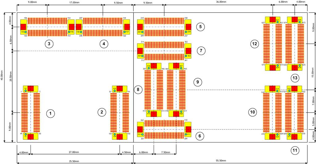
6 FPGA I/O details The following table lists in detail the number and configuration of available FPGA I/Os per bank. Con 8 includes the 32 data lines of the EBI2. This is not populated per default in order to protect the signal integrity of this interface. Bank 0 Bank 2 Bank 3 Con Single input Diff input Diff I/O Single input Diff input Diff I/O Single Input Diff input Diff I/O p/8s 2p/4s 2 2p/4s 4p/8s p/16s 8 16p/32s 9 16p/32s 10 16p/32s 11 16p/32s 12 16p/32s 13 16p/32s Sum Sum: 212 I/Os, 42 inputs, 254 overall For the XC3S700AN FPGA, the following restrictions apply: Single input pins can be used only as single-ended inputs Diff input pin (pairs) may be used as two single inputs or as one differential LVDS input pair Diff I/O pin (pairs) can be used as - Two single-ended inputs - Two single-ended outputs - One differential input pair - One differential output pair (only bank 0/2, bank 1/3 does not support differential outputs) Page 6
7 Pinout SAM9G45 (con 1 - ARM9) Port/Pin ARM9 Periphery on ARM9 Notice 1 GND GND 2 PA10 ETX0 3 PC0 DQM2 4 PA11 ETX1 5 PC1 DQM3 6 PA29 ECRS/MCI1_DA6 7 GND GND 8 PA26 ETH_RESETn/MCI1_DA3/TIOB2 9 GND GND 10 PA30 ECOL/MCI1_DA7 11 PD31 TIOB1/PWM1 12 PA25 ETH_PDWN/MCI1_DA2/PWM3 13 PD30 TIOB0/SCK2 14 PC6 ETH_MDINTRn/A23 15 PD28 SPI_NPCS1/TSADTRG 16 PA27 ETXER/MCI1_DA4 17 GND GND 18 PA6 ETX2/MCI0_DA4 19 PC0 USB2_PSWN/DQM2 20 PA7 ETX3/MCI0_DA5 21 PC1 USB2_OCN/DQM3 22 PA14 ETXEN 23 PC0 USB1_PSWN/DQM2 24 PA17 ETXCK 25 PC1 USB1_OCN/DQM3 26 PA12 ERX0 27 GND GND 28 PA13 ERX1 29 USB-Host3 + for use, place network resistor R90 30 PA8 ERX2/MCI0_DA6 31 USB-Host3 - for use, place network resistor R90 32 PA9 ERX3/MCI0_DA7 33 GND 34 PA16 ERXER 35 USB-Host2 + for use, place network resistor R89 36 PA28 ERXCK/MCI1_DA5 37 USB-Host2 - for use, place network resistor R89 38 PA15 ERXDV 39 GND 40 PA19 EMDIO 41 USB-Host1 + default USB-Host D+ Pin 42 PA18 EMDC/ETH_MDC 43 USB-Host1 - default USB-Host D Pin 44 GND 45 GND 46 GND 47 PE31 PCK1/PWM2 48 NC 49 GND 50 NC 51 NC non plated hole 52 NC non plated hole Page 7
8 Pinout SAM9G45 (con 2 - ARM9) Port/Pin ARM9 Periphery on ARM9 Notice 53 PD8 AC97FS/TIOB5 54 GND 55 PD7 AS97TX/TIOA5 56 HHSDMB/DHSDM Device- or Host- can be selected by Register 57 PD9 AC97CK/TCLK5 58 HHSDPB/DHSDP Device+ or Host+ can be selected by Register 59 PD6 AC97RX 60 GND 61 PB14 SPI1_MISO 62 GND 63 PB31 ISI_MCK/PCK1 64 GND 65 GND 66 GND 67 GND 68 TDI 69 PB11 ISI_DAT11/TWI1_SCL 70 NTRST 71 PB10 ISI_D10/TWI1_SDA 72 NC 73 PB9 ISI_D9/UART3_RXD 74 RESETn 75 PB8 ISI_D8/UART3_TXD 76 TMS 77 PB28 ISI_PCLK 78 TDO 79 PB29 ISI_VSYNC 80 TCK 81 PB30 ISI_HSYNC 82 GND 83 PB27 ISI_DAT7 84 GND 85 PB26 ISI_DAT6 86 GND 87 PB25 ISI_DAT5 88 PD3 RD0 89 PB24 ISI_DAT4 90 PD2 TD0 91 PB23 ISI_DAT3 92 PD1 TF0 93 PB22 ISI_DAT2 94 GND 95 PB21 ISI_DAT1 96 PD0 TK0/PWM3 97 PB20 ISI_DAT0 98 PD4 RK0 99 GND 100 PD5 RF0 101 GND 102 GND 103 NC non plated hole 104 NC non plated hole Page 8
9 Pinout SAM9G45 (con 3 - ARM9) Port/Pin ARM9 Periphery on ARM9 Notice 105 PE30 LCDD GND GND 107 PE29 LCDD PE23 LCDD16/LCDD PE28 LCDD PE22 LCDD15/LCDD PE27 LCDD PE21 LCDD14/LCDD GND 114 PE20 LCDD13/LCCD PE26 LCDD PE19 LCDD12/LCDD PE25 LCDD PE18 LCDD11/LCDD PE24 LCDD17/LCDD PE17 LCDD10/LCDD GND 122 PE16 LCDD9/LCDD GND 124 PE15 LCDD8/LCDD PD27 GPAD7/SPI0_NPCS3/PCK1 126 PE14 LCDD7/LCDD PD26 PCK0/PWM2/GPAD6 128 PE13 LCDD6/LCDD GND 130 PE12 LCDD5/LCDD7 131 PD23 TCLK0/TSAD3 132 PE11 LCDD4/LCDD6 133 PD22 TIOA2/TSAD2 134 PE10 LCDD3/LCDD5 135 PD21 TIOA1/TSAD1 136 PE9 LCDD2/LCDD4 137 GND 138 PE8 LCDDAT1/LCDD3 139 PD20 TIOA0/TSAD0 140 PE7 LCDD0/LCDD2 141 PD19 SPI1_NPCS3/FIQ 142 PE0 LCDPWR/PCK0 143 PD18 SPI1_NPCS2/IRQ 144 PE1 LCDMOD 145 GND 146 PE6 LCDDEN/LCDDVAL 147 PA24 MCI1_DA1/CTS3 148 PE3 LCDVSYNC 149 PA23 MCI1_DA0/RTS3 150 PE5 LCDDOTCK 151 PA22 MCI1_CDA/SCK3 152 PE4 LCDHSYNC 153 GND 154 PE2 LCDCC 155 NC NC non plated hole 156 NC NC non plated hole Page 9
10 Pinout SAM9G45 (con 4 - ARM9) Port/Pin ARM9 Periphery on ARM9 Notice 157 NC NC non plated hole 158 NC NC non plated hole 159 ARM9_EN 160 VCC_ARM9 +3.3V-5V 161 VCC_ARM9 +3.3V-5V 162 VCC_ARM9 +3.3V-5V 163 VCC_ARM9 +3.3V-5V 164 VCC_ARM9 +3.3V-5V 165 VCC_ARM9 +3.3V-5V 166 VCC_ARM9 +3.3V-5V 167 GND 168 GND 169 GND 170 GND 171 GND 172 GND 173 GND 174 GND 175 WKUP WAKEN use a 10K pullup 176 GND enables voltage regualtors, connect to VCC for normal operation 177 NRST RESET_OUT use a button to ground for reset 178 PB16 SPI1_SPCK/SCK0 179 PD29 TCLK1/SCK1 180 PB18 RXD0/SPI0_NPCS1 181 PB5 RXD1 182 PB19 TXD0/SPI0_NPCS2 183 GND 184 PB15 CTS0/SPI1_MOSI 185 PB4 TXD1 186 PB17 RTS0/SPI1_NPCS0 187 PD16 RTS1 188 GND 189 PD17 CTS1 190 PB6 TXD2 191 GND 192 PB7 RXD2 193 PB12 DRXD 194 PA20 TWD0 195 PB13 DTXD 196 PA21 TWCK0 197 PB0 SPI0_MISO 198 PA0 MCI0_CK/TCLK3 199 PB1 SPI0_MOSI 200 PA1 MCI0_CDA/TIOA3 201 PB2 SPI0_SCK 202 PA2 MCI0_DA0/TIOB3 203 PB3 SPI0_NPCS0 204 PA3 MCI0_DA1/TCLK4 205 PD24 SPI0_NPCS1/PWM0/GPAD4 206 PA4 MCI0_DA2/TIOA4 207 PD25 SPI0_NPCS2/PWM1/GPAD5 208 PA5 MCI0_DA3/TIOB4 Page 10
11 Pinout XC3S700AN (con 5 - supply+jtag) BALL NAME Signal Name Notice 209 VCC_FPGA +3.3V-5V 210 VCC_FPGA +3.3V-5V 211 VCC_FPGA +3.3V-5V 212 VCC_FPGA +3.3V-5V 213 VCC_FPGA +3.3V-5V 214 FPGA_En enables voltage regulators, connect to VCC for normal operation 215 VCC_FPGA +3.3V-5V 216 GND 217 VCC_FPGA +3.3V-5V 218 F5 TDI 219 VCC_FPGA +3.3V-5V 220 A21 TCK 221 VCC_FPGA +3.3V-5V 222 GND 223 VCC_FPGA +3.3V-5V 224 E19 TDO 225 VCC_FPGA +3.3V-5V 226 D4 TMS 227 VCCO_3 +3.3V 228 GND 229 VCCO_3 +3.3V 230 V13 FPGA_INITB/ IO_L26P 231 VCCO_3 +3.3V 232 Y VCCO_3 +3.3V 234 GND 235 VCCO_3 +3.3V 236 GND 237 VCCO_3 +3.3V 238 GND 239 VCCO_3 +3.3V 240 GND 241 VCCO_3 +3.3V 242 GND 243 VCCO_0 +3.3V 244 GND 245 VCCO_0 +3.3V 246 GND 247 VCCO_0 +3.3V 248 GND 249 VCCO_0 +3.3V 250 GND 251 VCCO_0 +3.3V 252 GND 253 VCCO_0 +3.3V 254 GND 255 VCCO_0 +3.3V 256 GND 257 VCCO_0 +3.3V 258 GND 259 NC non plated hole 260 NC non plated hole Page 11
12 Pinout XC3S700AN (con 6 - bank 0/2/3 I/Os) 261 GND 262 GND BALL NAME Signal Name Notice 263 AA1 IO_L45P_3 264 U18 SUSPEND high input for suspend mode activation (only if bit is set) 265 AA2 IO_L45N_3 266 C4 PROG_B 267 GND 268 GND 269 Y1 IO_L44P_3 270 AB15 IO_L24P_2/Awake awake is a open-drain output (the default), if suspend mode is active 271 Y2 IO_L44N_3 272 AA15 IO_L24N_2/DOUT 273 GND 274 GND 275 V4 IO_L43P_3 276 U11 IO_L17P_2/GCLK W3 IO_L43N_3 278 V11 IO_L17N_2/GCLK GND 280 GND 281 W1 IO_L42P_3 282 J7 IP_L11P_3 283 W2 IO_L42N_3 284 K8 IP_L11N_3 285 GND 286 GND 287 B2 IO_L36P_0 288 H8 IP_L04P_3 289 A2 IO_L36N_0/PDUC_B 290 H7 IP_L04N_3/VREF_3 291 GND 292 GND 293 F7 IO_L35P_0 294 J8 IP02_3/VREF_3 295 E6 IO_L35N_0 296 R6 IP01_3/VREF_3 297 GND 298 GND 299 E7 IO_L34P_0 300 F12 IP04_0 301 F8 IO_L34N_0 302 F10 IP03_0 303 GND 304 GND 305 A3 IO_L33P_0 306 E8 IP02_0 307 B3 IO_L33N_0 308 E16 IP01_0 309 GND 310 GND 311 NC non plated hole 312 NC non plated hole Page 12
13 Pinout XC3S700AN (con 7 - bank0+3 inputs) BALL NAME Signal Name Notice 313 GND 314 GND 315 H9 IP20_0/VREF_0 316 R7 IP_L46P_3 317 H12 IP19_0/VREF_0 318 T6 IP_L46N_3/VREF_3 319 GND 320 GND 321 G8 IP18_0/VREF_0 322 P7 IP_L39P_3 323 H14 IP17_0 324 R8 IP_L39N_3 325 GND 326 GND 327 H13 IP16_0 328 N7 IP_L35P_3 329 H10 IP15_0 330 P8 IP_L35N_3 331 GND 332 GND 333 G9 IP14_0 334 N6 IP_L31P_3 335 G7 IP13_0 336 N5 IP_L31N_3 337 GND 338 GND 339 G16 IP12_0 340 N8 IP_L27P_3 341 G15 IP11_0 342 N9 IP_L27N_3 343 GND 344 GND 345 G14 IP10_0 346 M7 IP_L23P_3 347 G13 IP09_0 348 M6 IP_L23N_3 349 GND 350 GND 351 G12 IP08_0 352 L7 IP_L19P_3 353 G11 IP07_0 354 M8 IP_L19N_3 355 GND 356 GND 357 G10 IP06_0 358 K7 IP_L15P_3 359 F16 IP05_0 360 L8 IP_L15N_3/VREF_3 361 GND 362 GND 363 NC non plated hole 364 NC non plated hole Page 13
14 Pinout XC3S700AN (con 8 - bank2 I/O)* 365 GND 366 GND BALL NAME Signal Name Notice 367 AA17 IO_L28P_2/D2 368 AB20 IO_L36P_2/D0/DIN/MISO 369 Y17 IO_L28N_2/D1 370 AA20 IO_L36N_2/CCLK 371 GND 372 GND 373 AB16 IO_L27P_2 374 AB21 IO_L35P_2 375 Y16 IO_L27N_2 376 AA21 IO_L35N_2 377 GND 378 GND 379 W15 IO_L25P_2 380 Y18 IO_L34P_2 381 Y15 IO_L25N_2 382 W17 IO_L34N_2 383 GND 384 GND 385 W13 IO_L23P_2 386 W18 IO_L33P_2 387 Y14 IO_L23N_2 388 V17 IO_L33N_2 389 GND 390 GND 391 AA14 IO_L22P_2 392 AB19 IO_L32P_2 393 AB14 IO_L22N_2/MOSI/CSI_B 394 AA19 IO_L32N_2 395 GND 396 GND 397 AB13 IO_L21P_2 398 W16 IO_L31P_2 399 Y13 IO_L21N_2 400 V16 IO_L31N_2 401 GND 402 GND 403 V12 IO_L20P_2/GCLK2 404 V14 IO_L30P_2 405 U12 IO_L20N_2/GCLK3 406 V15 IO_L30N_2 407 GND 408 GND 409 W12 IO_L18P_2/GCLK AB17 IO_L29P_2 411 Y12 IO_L18N_2/GCLK AB18 IO_L29N_2 413 GND 414 GND 415 NC non plated hole 416 NC non plated hole * This is only available when the ARM9 on the OEM module is not used Page 14
15 Pinout XC3S700AN (con 9 - bank2 I/O) BALL NAME Signal Name Notice 417 GND 418 GND 419 AA6 IO_L08P_2 420 Y11 IO_L16P_2/D5 421 AB6 IO_L08N_2 422 AB11 IO_L16N_2/D4 423 GND 424 GND 425 W7 IO_L07P_2 426 AA10 IO_L15P_2 427 Y6 IO_L07N_2 428 AB10 IO_L15N_2 429 GND 430 GND 431 AB4 IO_L06P_2 432 Y9 IO_L14P_2/D7 433 AB5 IO_L06N_2 434 AB9 IO_L14N_2/D6 435 GND 436 GND 437 W6 IO_L05P_2 438 V10 IO_L13P_2 439 Y5 IO_L05N_2 440 Y10 IO_L13N_2 441 GND 442 GND 443 AB3 IO_L04P_2 444 AA8 IO_L12P_2 445 AA4 IO_L04N_2 446 AB8 IO_L12N_2 447 GND 448 GND 449 AB2 IO_L03P_2 450 W8 IO_L11P_2/VS1 451 AA3 IO_L03N_2 452 Y8 IO_L11N_2/VS0 453 GND 454 GND 455 W4 IO_L02P_2/M2 456 Y7 IO_L10P_2 457 Y4 IO_L02N_2/CSO_B 458 AB7 IO_L10N_2 459 GND 460 GND 461 V6 IO_L01P_2/M1 462 V9 IO_L09P_2/RDWR_B 463 W5 IO_L01N_2/M0 464 W9 IO_L09N_2/VS2 465 GND 466 GND 467 NC non plated hole 468 NC non plated hole Page 15
16 Pinout XC3S700AN (con 10 - bank0 I/O) BALL NAME Signal Name Notice 469 GND 470 GND 471 D16 IO_L08P_0 472 B13 IO_L16P_0 473 C16 IO_L08N_0 474 A13 IO_L16N_0 475 GND 476 GND 477 D17 IO_L07P_0 478 D13 IO_L15P_0 479 C17 IO_L07N_0 480 C13 IO_L15N_0 481 GND 482 GND 483 B19 IO_L06P_0/VREF_0 484 F13 IO_L14P_0 485 A19 IO_L06N_0 486 E13 IO_L14N_0 487 GND 488 GND 489 C18 IO_L05P_0 490 B15 IO_L13P_0 491 A18 IO_L05N_0 492 A14 IO_L13N_0 493 GND 494 GND 495 E15 IO_L04P_0 496 A16 IO_L12P_0 497 F15 IO_L04N_0 498 A15 IO_L12N_0/VREF_0 499 GND 500 GND 501 B20 IO_L03P_0 502 D15 IO_L11P_0 503 A20 IO_L03N_0 504 C15 IO_L11N_0 505 GND 506 GND 507 D19 IO_L02P_0/VREF_0 508 B17 IO_L10P_0 509 C19 IO_L02N_0 510 A17 IO_L10N_0 511 GND 512 GND 513 E17 IO_L01P_0 514 C14 IO_L09P_0 515 D18 IO_L01N_0 516 E14 IO_L09N_0 517 GND 518 GND 519 NC non plated hole 520 NC non plated hole Page 16
17 Pinout XC3S700AN (con 11 - bank0 I/O) BALL NAME Signal Name Notice 521 GND 522 GND 523 B9 IO_L24P_0 524 C5 IO_L32P_0 525 C9 IO_L24N_0/VREF_0 526 D5 IO_L32N_0 527 GND 528 GND 529 D10 IO_L23P_0 530 A4 IO_L31P_0 531 E10 IO_L23N_0 532 B4 IO_L31N_0 533 GND 534 GND 535 A9 IO_L22P_0 536 E9 IO_L30P_0 537 A8 IO_L22N_0 538 D8 IO_L30N_0 539 GND 540 GND 541 A10 IO_L21P_0 542 C6 IO_L29P_0 543 C10 IO_L21N_0 544 D6 IO_L29N_0 545 GND 546 GND 547 D11 IO_L20P_0/GCLK B6 IO_L28P_0 549 E11 IO_L20N_0/GCLK A5 IO_L28N_0 551 GND 552 GND 553 B11 IO_L19P_0/GCLK8 554 D7 IO_L27P_0 555 C11 IO_L19N_0/GCLK9 556 C7 IO_L27N_0 557 GND 558 GND 559 A12 IO_L18P_0/GCLK6 560 A7 IO_L26P_0 561 A11 IO_L18N_0/GCLK7 562 A6 IO_L26N_0 563 GND 564 GND 565 C12 IO_L17P_0/GCLK4 566 B8 IO_L25P_0 567 E12 IO_L17N_0/GCLK5 568 C8 IO_L25N_0 569 GND 570 GND 571 NC non plated hole 572 NC non plated hole Page 17
18 Pinout XC3S700AN (con 12 - bank3 I/O) BALL NAME Signal Name Notice 573 GND 574 GND 575 M5 IO_L30P_3 576 U3 IO_L41P_3 577 N4 IO_L30N_3 578 U4 IO_L41N_3 579 GND 580 GND 581 P3 IO_L29P_3 582 T5 IO_L40P_3 583 P5 IO_L29N_3 584 U5 IO_L40N_3 585 GND 586 GND 587 P1 IO_L28P_3 588 V1 IO_L38P_3 589 P2 IO_L28N_3 590 V3 IO_L38N_3 591 GND 592 GND 593 N1 IO_L26P_3/VREF_3 594 U1 IO_L37P_3 595 N3 IO_L26N_3 596 U2 IO_L37N_3 597 GND 598 GND 599 M3 IO_L25P_3/TRDY2/LHCLK6 600 T1 IO_L36P_3/VREF_3 601 M4 IO_L25N_3/LHCLK7 602 T3 IO_L36N_3 603 GND 604 GND 605 M1 IO_L24P_3/LHCLK4 606 R5 IO_L34P_3 607 M2 IO_L24N_3/LHCLK5 608 T4 IO_L34N_3 609 GND 610 GND 611 K1 IO_L22P_3/LHCLK2 612 R3 IO_L33P_3 613 L1 IO_L22N_3/IRDY2/LHCLK3 614 R4 IO_L33N_3 615 GND 616 GND 617 L5 IO_L21P_3/LHCLK0 618 R1 IO_L32P_3 619 L3 IO_L21N_3/LHCLK1 620 R2 IO_L32N_3 621 GND 622 GND 623 NC non plated hole 624 NC non plated hole Page 18
19 Pinout XC3S700AN (con 13 - bank3 I/O) BALL NAME Signal Name Notice 625 GND 626 GND 627 H5 IO_L09P_3 628 K3 IO_L20P_3 629 H6 IO_L09N_3 630 K2 IO_L20N_3 631 GND 632 GND 633 F3 IO_L08P_3 634 K5 IO_L18P_3 635 G4 IO_L08N_3 636 K4 IO_L18N_3 637 GND 638 GND 639 F4 IO_L07P_3 640 J3 IO_L17P_3 641 E3 IO_L07N_3 642 J1 IO_L17N_3/VREF_3 643 GND 644 GND 645 D1 IO_L06P_3 646 H2 IO_L16P_3 647 E1 IO_L06N_3 648 H1 IO_L16N_3 649 GND 650 GND 651 G6 IO_L05P_3 652 H4 IO_L14P_3 653 G5 IO_L05N_3 654 H3 IO_L14N_3 655 GND 656 GND 657 D3 IO_L03P_3 658 G3 IO_L13P_3 659 E4 IO_L03N_3 660 G1 IO_L13N_3 661 GND 662 GND 663 B1 IO_L02P_3 664 F2 IO_L12P_3 665 C2 IO_L02N_3 666 F1 IO_L12N_3 667 GND 668 GND 669 C1 IO_L01P_3 670 K6 IO_L10P_3 671 D2 IO_L01N_3 672 J5 IO_L10N_3 673 GND 674 GND 675 NC non plated hole 676 NC non plated hole Page 19

20 Evaluation and Development Complementary to the ICnova SAM9G45+XC3S700AN OEM, we offer the evaluation board ADB3000 and a corresponding starter kit with OEM board and 5 display. Among others, the ADB3000 offers the following features: All FPGA I/Os available on pin headers Two high-speed s with 12 differential pairs each plus ground Integrated OpenOCD debugger und debug-uart for ARM via mini-usb Power supply can be done using a wall power supply, a lab supply using banana jacks or USB Ethernet, µsd, USB Host, USB Slave and many more... More details can be found in the ADB3000 datasheet. Page 20
21 Ordering information Description Article number Packaging Min order quantity ICnova SAM9G45+XC3S700AN ESD-bag, air cushion 1 Besides corresponding evaluation boards, we also offer: Hardware design of base boards optimized for your application Prototype and mass production using our internal production lines Adaptation / assembly options of our standard products Linux driver development and adaptation FPGA design services including integration with corresponding (test-) software are available through our competent partner Loginovo GmbH. Contact info@in-circuit.de Change history Version Date Changes Editor A 08/25/2010 First version Gassmann B 09/15/2010 Added page for required software, source codes and documentation Gassmann D 09/16/2011 Inserted corrected footprint, distance between 8 and 9 was wrong. Stopped maintaining German version. E 01/27/2012 Corrected name of pin 270 (awake), was named 24N, but is 24P. Translated remaining german footnote on page 14 to English. Flipped Con9 pins, were mirrored before. Gassmann Gassmann Page 21
ICnova SAMA5D37 SODIMM Datasheet
 SAMA5D37 SODIMM-200 Module Cost eficient, high performance, reliable + Guaranteed availability >5 years (with customer outline agreement) + Easy design-in at low risk + Cost saving by short development
ICnova SAM9G45 SODIMM Datasheet
 SAM9G45-200 Module Cost eficient, high performance, reliable + Guaranteed availability >5 years (with customer outline agreement) + Easy design-in at low risk + Cost saving by short development cycles
MYC-SAMA5D3X CPU Module
 MYC-SAMA5D3X CPU Module - 536MHz Atmel SAMA5D3 Series ARM Cortex-A5 Processors - 512MB DDR2 SDRAM (256MB is optional) - 256MB Nand Flash, 16MB Nor Flash, 4MB Data Flash - On-board Gigabit Ethernet PHY
Elbert V2 Spartan 3A FPGA Development Board. User Guide. Rev 9
 Elbert V Spartan A FPGA Development Board User Guide Rev 9 Get in touch with us! Please feel free to send a mail to one of the mail IDs below or use the Contact Us page at http:// to drop us a quick message.
AT91SAM9G45 EVK Board
 AT91SAM9G45 EVK Board User Manual V1.0 date:2011.02.22 Revision history Rev Date Description 1.0 20110222 Initial version Catalog SECTION 1 OVERVIEW... 1 1.1 Scope... 1 1.2 Deliverables... 1 1.3 The AT91SAM9G45-EVK
Glomation. Evaluation Carrier Board GECB-9GX5 Quick Start Guide
 Glomation Evaluation Carrier Board GECB-9GX5 Quick Start Guide Table of Contents Chapter 1 Introducing the GECB-9GX5 Carrier Board... 4 GECB-9GX5 Overview... 4 Integrated Features... 4 Chapter 2 GECB-9GX5
WT-ARM9G25-S1 core board datasheet
 WT-ARM9G25-S1 core board datasheet WT-ARM9G25-S1 Overview WT-ARM9G25-S1 core module is an industrial embedded core board based on ATMEL AT91SAM9G25 ARM9 CPU, which adopts SMT package, 4cm x 4cm ultra small
Mimas Spartan 6 FPGA Development Board. User Guide. Rev 9
 Mimas Spartan 6 FPGA Development Board User Guide Rev 9 Get in touch with us! Please feel free to send a mail to one of the mail IDs below or use the Contact Us page at http:// to drop us a quick message.
COM-RZN1D - Hardware Manual
 COM-RZN1D - Hardware Manual Hardware Manual 4 / 01.10.2018 emtrion GmbH Copyright 2018 emtrion GmbH All rights reserved. This documentation may not be photocopied or recorded on any electronic media without
Intel Galileo gen 2 Board
 Intel Galileo gen 2 Board The Arduino Intel Galileo board is a microcontroller board based on the Intel Quark SoC X1000, a 32- bit Intel Pentium -class system on a chip (SoC). It is the first board based
GLOMATION. Embedded Single Board Computer GESBC-9G10 User s Manual
 GLOMATION Embedded Single Board Computer GESBC-9G10 User s Manual Table of Contents Chapter 1 Introducing the GESBC-9G10 Single Board Computer... 4 GESBC-9G10 Overview... 4 Advanced Features... 4 AT91SAM9G10...
EV-9X35-NANO System on Module
 Evodbg EV-9X35-NANO System on Module User manual Revision 1.0 2-1-2016 EV- 9 X 3 5 - N A N O w w w. e v o d b g. c o m P a g e 1 TABLE OF CONTENTS Table of contents... 1 Attention!... 3 Important Information
LEAD FREE FEATURES: Rev. 1.7 (May 2011) 1 DLP Design, Inc.
 1 DLP Design, Inc.") USB - FPGA MODULE DLP-HS-FPGA DLP-HS-FPGA LEAD FREE FEATURES: Xilinx XCS00A-FTGC FPGA utilized on the DLP-HS-FPGA Xilinx XCS00A-FTGC FPGA utilized on the DLP-HS-FPGA Micron M x DDR SDRAM Memory Built-In
USB - FPGA MODULE DLP-HS-FPGA DLP-HS-FPGA LEAD FREE FEATURES: Xilinx XCS00A-FTGC FPGA utilized on the DLP-HS-FPGA Xilinx XCS00A-FTGC FPGA utilized on the DLP-HS-FPGA Micron M x DDR SDRAM Memory Built-In
Cookie User Manual. For NuMicro Edition 1.0. Rev. 1.0 Release: forum.coocox.org.
 Cookie User Manual For NuMicro Edition 1.0 Rev. 1.0 Release: 2012-08-09 Website: Forum: Techinal: Market: www.coocox.org forum.coocox.org master@coocox.com market@coocox.com 1 Introduction Cookie is an
LEAD-FREE FEATURES: Rev. 2.0 (Sep 2015) 1 DLP Design, Inc.
 1 DLP Design, Inc.") DLP-HS- FPGA-A LEAD-FREE USB - FPGA MODULE (PRELIMINARY) FEATURES: Xilinx XCS00A-FTGC FPGA Micron M x DDR SDRAM Memory Built-In Configuration Loader; Writes the Bit File Directly to SPI Flash via High-Speed
DLP-HS- FPGA-A LEAD-FREE USB - FPGA MODULE (PRELIMINARY) FEATURES: Xilinx XCS00A-FTGC FPGA Micron M x DDR SDRAM Memory Built-In Configuration Loader; Writes the Bit File Directly to SPI Flash via High-Speed
AT-501 Cortex-A5 System On Module Product Brief
 AT-501 Cortex-A5 System On Module Product Brief 1. Scope The following document provides a brief description of the AT-501 System on Module (SOM) its features and ordering options. For more details please
AT-501 Cortex-A5 System on Module Integration guide
 AT-501 Cortex-A5 System on Module Integration guide Revision 1.0 Contents 1. Scope... 4 1.1 SoM introduction... 4 1.2 SoM models... 4 2. AT-501 Integration guide... 6 1.3 Power connectivity... 6 1.4 Reset...
Teratronik elektronische systeme gmbh. V4½-CPU Technical Data. Date:
 Teratronik elektronische systeme gmbh Technical Data Date: 2008-11-26 Table of contents 1. 2. 3. 3.1 3.2 3.3 3.4 3.5 3.6 3.7 3.8 4. 4.1 4.2 4.3 4.4 Features...3 Views...4 Connector pinouts...6 J1 - board-to-board
EMX Module Specifications
 EMX is a combination of hardware (ARM Processor, Flash, RAM, Ethernet PHY...etc) on a very small (1.55 x1.8 ) SMT OEM 8-Layer board that hosts Microsoft.NET Micro Framework with various PAL/HAL drivers.
GODIL USER MANUAL V 0.9 OHO-Elektronik
 GODIL USER MANUAL V 0.9 OHO-Elektronik www.oho-elektronik.de Author: M.Randelzhofer OHO-Elektronik Michael Randelzhofer Rudolf-Diesel-Str. 8 85221 Dachau Germany WEB: www.oho-elektronik.de EMAIL: info@oho-elektronik.de
MYD-IMX28X Development Board
 MYD-IMX28X Development Board MYC-IMX28X CPU Module as Controller Board Two 1.27mm pitch 80-pin SMT Male Connectors for Board-to-Board Connections 454MHz Freescale i.mx28 Series ARM926EJ-S Processors 128MB
3.3V regulator. JA H-bridge. Doc: page 1 of 7
 Digilent Cerebot Board Reference Manual Revision: 11/17/2005 www.digilentinc.com 215 E Main Suite D Pullman, WA 99163 (509) 334 6306 Voice and Fax Overview The Digilent Cerebot Board is a useful tool for
Xilinx Spartan 6 + DDR3 DIMM development boards
 Xilinx Spartan 6 + DDR3 DIMM development boards Introduction The SiOI are a family of Xilinx Spartan 6 FPGA development boards with support for FPGAs of medium to large size, up to 8GB of DRAM and six
Lima (-I) Data sheet. Lima has N 2x2 radio supporting up to 300 Mbps data-rate and comes in two versions: commercial or industrial temperature
 Data sheet. Lima has N 2x2 radio supporting up to 300 Mbps data-rate and comes in two versions: commercial or industrial temperature") (-I) has 802.11N 2x2 radio supporting up to 300 Mbps data-rate and comes in two versions: commercial or industrial temperature is a QCA 4531 chipset based module with a 650 MHz CPU and 802.11N 2x2 (MIMO)
(-I) has 802.11N 2x2 radio supporting up to 300 Mbps data-rate and comes in two versions: commercial or industrial temperature is a QCA 4531 chipset based module with a 650 MHz CPU and 802.11N 2x2 (MIMO)
Hardware Reference. DIL/NetPC DNP/9265 Board Revision 1.0
 DIL/NetPC DNP/9265 Board Revision 1.0 Hardware Reference SSV Embedded Systems Dünenweg 5 D-30419 Hannover Phone: +49 (0)511/40 000-0 Fax: +49 (0)511/40 000-40 E-mail: sales@ssv-embedded.de Document Revision:
Evaluating SiFive RISC- V Core IP
 Evaluating SiFive RISC- V Core IP Drew Barbier January 2018 drew@sifive.com 3 Part Webinar Series Webinar Recordings and Slides: https://info.sifive.com/risc-v-webinar RISC-V 101 The Fundamentals of RISC-V
A NEW VISION OF THE EMBEDDED WORLD APF27DEV APF27DEV DATASHEET 0.H
 A NEW VISION OF THE EMBEDDED WORLD APF27DEV APF27DEV DATASHEET 0.H 26. juillet 2012 Disclaimer The informations in this manual have been carefully checked and are believed to be accurate. Armadeus systems
User Manual For CP-JR ARM7 USB-LPC2148 / EXP
 CP-JR ARM7 USB-LPC2148 / EXP 38 CR-JR ARM7 USB-LPC2148 which is a Board Microcontroller ARM7TDMI-S Core uses Microcontroller 16/32-Bit 64 Pin as Low Power type to be a permanent MCU on board and uses MCU
EVAcharge SE - datasheet
 EVAcharge SE - datasheet Data Sheet (valid for board revision V0R4 or higher) Document history Revision 1.0 2013-10-10 Initial release 1.1 2013-11-06 Typo corrections 1.2 2014-05-13 Removed serial IF 1.3
Hardware Specification. Figure 1-2 ZYNQ-7000 Device Family 2 / 9
 Z-turn Board 667MHz Xilinx XC7Z010/20 Dual-core ARM Cortex-A9 Processor with Xilinx 7-series FPGA logic 1GB DDR3 SDRAM (2 x 512MB, 32-bit), 16MB SPI Flash USB_UART, USB2.0 OTG, 1 x 10/100/1000Mbps Ethernet,
pico-sam9g45 System board
 System board Reference manual Rev. 1.j Layout Views Layout top view Layout bottom view Legend: J2 Ethernet port J12 ZIF connector for the LCD U1 USB HUB SMSC chip J3 USB 2.0 J14 Keypad connector BEEP PWM
FPGA Board Reference Guide. Author: Rico Möckel Supervisor: Prof. Auke Jan Ijspeert
 FPGA Board Reference Guide Author: Supervisor: Prof. Auke Jan Ijspeert FPGA Board Reference Guide Date Version Changes October 18, 2004 1.0 - Page 2 Table of Contents Purpose... 4 Audience... 4 Organization...
DevKit7000 Evaluation Kit
 DevKit7000 Evaluation Kit Samsung S5PV210 Processor based on 1GHz ARM Cortex-A8 core Onboard 512MByte DDR2 and 512MByte NAND Flash 4 UART, 4 USB Host, USB Device, Ethernet, Audio, TF, RTC,... Supports
FriendlyARM. Mini2440.
 FriendlyARM Mini2440 www.friendlyarm.net 1 Introduction...3 1.1 Features...4 2 Hardware Resource...6 2.1 Jumpers and Interfaces...6 2.2 Memory Map...7 2.2.1 Memory Adress Allocation...7 2.3 Power Supply...8
Wireless Sensor Networks. FireFly 2.2 Datasheet
 2.2 Datasheet July 6, 2010 This page intentionally left blank. Contents 1. INTRODUCTION...1 Features...1 Applications...2 2. BLOCK DIAGRAM...3 3. HARDWARE CONNECTIONS...4 Power...5 Header 1 ( UARTS, I2C,
Revision: 5/7/ E Main Suite D Pullman, WA (509) Voice and Fax. Power jack 5-9VDC. Serial Port. Parallel Port
 Voice and Fax. Power jack 5-9VDC. Serial Port. Parallel Port") Digilent Digilab 2 Reference Manual www.digilentinc.com Revision: 5/7/02 215 E Main Suite D Pullman, WA 99163 (509) 334 6306 Voice and Fax Overview The Digilab 2 development board (the D2) features the
Digilent Digilab 2 Reference Manual www.digilentinc.com Revision: 5/7/02 215 E Main Suite D Pullman, WA 99163 (509) 334 6306 Voice and Fax Overview The Digilab 2 development board (the D2) features the
Product Specification
 Product Specification 15mm x 27mm Description One of the most capable Bluetooth modules available, the BT-21 Bluetooth OEM Module is designed for maximum flexibility. The BT-21 module includes 14 general
LEAD FREE FEATURES: Rev. 1.1 (April 2012) 1 DLP Design, Inc.
 1 DLP Design, Inc.") DLP-HS-FPGA LEAD FREE USB - FPGA MODULE FEATURES: Xilinx XCS00A-FTGC FPGA Utilized on the DLP-HS-FPGA Micron M x 8 DDR SDRAM Memory Built-In Configuration Loader; Writes the Bit File Directly to SPI Flash
DLP-HS-FPGA LEAD FREE USB - FPGA MODULE FEATURES: Xilinx XCS00A-FTGC FPGA Utilized on the DLP-HS-FPGA Micron M x 8 DDR SDRAM Memory Built-In Configuration Loader; Writes the Bit File Directly to SPI Flash
Digilab 2E Reference Manual
 Digilent 2E System Board Reference Manual www.digilentinc.com Revision: February 8, 2005 246 East Main Pullman, WA 99163 (509) 334 6306 Voice and Fax Digilab 2E Reference Manual Overview The Digilab 2E
Digilab 2 Reference Manual
 125 SE High Street Pullman, WA 99163 (509) 334 6306 (Voice and Fax) www.digilentinc.com PRELIMINARY Digilab 2 Reference Manual Revision: November 19, 2001 Overview The Digilab 2 (D2) development board
Various power connectors. 3.3V regulator. 64K Flash (Internal) 2K EEPROM (Internal) 4K SRAM (Internal) JA Mem Adr/ Data. Doc: page 1 of 9
 2K EEPROM (Internal) 4K SRAM (Internal) JA Mem Adr/ Data. Doc: page 1 of 9") Cerebot II Board Reference Manual Revision: September 14, 2007 Note: This document applies to REV B of the board. www.digilentinc.com 215 E Main Suite D Pullman, WA 99163 (509) 334 6306 Voice and Fax Overview
Cerebot II Board Reference Manual Revision: September 14, 2007 Note: This document applies to REV B of the board. www.digilentinc.com 215 E Main Suite D Pullman, WA 99163 (509) 334 6306 Voice and Fax Overview
MYD-Y6ULX Development Board
 MYD-Y6ULX Development Board MYC-Y6ULX CPU Module as Controller Board 528Hz NXP i.mx 6UL/6ULL ARM Cortex-A7 Processors 1.0mm pitch 140-pin Stamp Hole Expansion Interface for Board-to-Board Connections 256MB
Introduction. Rev.1.2
 Introduction The Revelation board is an evaluation tool which is designed to help to start working with Riverdi TFT panels with FT8XX controllers. It can also be used as a platform to build your own application.
MYD-SAM9X5 Development Board
 MYD-SAM9X5 Development Board MYC-SAM9X5 CPU Module as Controller Board and Fully Compatible with Atmel s Official Board 400MHz Atmel AT91SAM9X5 Series ARM926EJ-S Processors 128MB DDR2 SDRAM, 256MB Nand
Taming the Beast. A simplified approach to working with FPGAs
 Projects Taming the Beast A simplified approach to working with FPGAs Text: Clemens Valens (Elektor Labs) Design: Raymond Vermeulen (Elektor Labs) FPGAs are unquestionably among the most versatile but
Hardware User Manual CM-BF561 V1.2, V Maximum Power at Minimum Size
 Hardware User Manual CM-BF561 V1.2, V1.3 Contact Bluetechnix Mechatronische Systeme GmbH Waidhausenstr. 3/19 A-1140 Vienna AUSTRIA/EUROPE office@bluetechnix.at http://www.bluetechnix.com Document No.:
Human Machine Interface Platform
 Human Machine Interface Platform J 0977M N01 (Preliminary) Deqing Jiahe Electronic Technology Co., Ltd. TEL: +86 572 8051676 ext. 803 FAX: +86 572 8051676 ext. 801 sales@jiahe electronic.com Version V1.0
)8-,768'HY.LW 2YHUYLHZ. )XMLWVX0LNURHOHNWURQLN*PE+ Am Siebenstein Dreieich-Buchschlag, Germany
8-,768'HY.LW 2YHUYLHZ. )XMLWVX0LNURHOHNWURQLN*PE+ Am Siebenstein Dreieich-Buchschlag, Germany") )8-,768'HY.LW 2YHUYLHZ )XMLWVX0LNURHOHNWURQLN*PE+ Am Siebenstein 6-10 63303 Dreieich-Buchschlag, Germany Revision: V1.0 Date: 05.08.1999 Introduction to FUJITSU Development Kit for 16LX CPU family DevKit16
)8-,768'HY.LW 2YHUYLHZ )XMLWVX0LNURHOHNWURQLN*PE+ Am Siebenstein 6-10 63303 Dreieich-Buchschlag, Germany Revision: V1.0 Date: 05.08.1999 Introduction to FUJITSU Development Kit for 16LX CPU family DevKit16
Centipede. Datasheet. Centipede is QCA AR9331 SoC based DIP platform with an integrated 2.4 GHz N (1x1) radio
 radio") is QCA AR9331 SoC based DIP platform with an integrated 2.4 GHz (1x1) radio Its tiny form factor (22 x 60 mm), integrated RJ-45, an on-board omni-directional chip antenna and "breadboardable" layout allows
is QCA AR9331 SoC based DIP platform with an integrated 2.4 GHz (1x1) radio Its tiny form factor (22 x 60 mm), integrated RJ-45, an on-board omni-directional chip antenna and "breadboardable" layout allows
MYD-IMX28X Development Board
 MYD-IMX28X Development Board MYC-IMX28X CPU Module as Controller Board Two 1.27mm pitch 80-pin SMT Connectors for Board-to-Board Connections 454MHz Freescale i.mx28 Series ARM926EJ-S Processors 128MB DDR2
Glomation. Embedded CPU Module GECM-5100 User s Manual
 Glomation Embedded CPU Module GECM-5100 User s Manual Table of Contents Chapter 1 Introducing the GECM-5100 CPU Module... 4 GECM-5100 Overview... 4 Advanced Features... 4 Chapter 2 GECM-5100 Function Blocks...
Embedded Systems Laboratory Manual ARM 9 TDMI
 Embedded Systems Laboratory Manual ARM 9 TDMI 1. Laboratory Rules a) Laboratory assessment: Presence during the laboratory is mandatory. One time unexcused absence is allowed within the semester. Students
SP601 Standalone Applications
 SP601 Standalone Applications December 2009 Copyright 2009 Xilinx XTP053 Note: This presentation applies to the SP601 Overview Xilinx SP601 Board Software Requirements SP601 Setup Multi-pin Wake-up GPIO
Product Specification
 Product Specification Features Amp ed RF, Inc. Description 15mm x 27mm The added class 1 power, +18dBm, of the BT-11, gives this module one of the best ranges in the industry. It s completely pin compatible
Product Technical Brief S3C2413 Rev 2.2, Apr. 2006
 Product Technical Brief Rev 2.2, Apr. 2006 Overview SAMSUNG's is a Derivative product of S3C2410A. is designed to provide hand-held devices and general applications with cost-effective, low-power, and
DATASHEET. MK-070C-HP High Performance 7 Inch Capacitive Touch Display. Amulet. Technologies. July 2015 Revision A
 High Performance 7 Inch Capacitive Touch Display DATASHEET July 2015 Revision A Introduction The MK-070C is the newest family member in the Display Module product line. The new 7 Capacitive Display Module
BT-22 Product Specification
 BT-22 Product Specification Features Amp ed RF, Inc. Description 10.4 mm x 13.5 mm Our micro-sized Bluetooth module is the smallest form factor available providing a complete RF platform. The BT-22 is
The industrial technology is rapidly moving towards ARM based solutions. Keeping this in mind, we are providing a Embedded ARM Training Suite.
 EMBEDDED ARM TRAINING SUITE ARM SUITE INCLUDES ARM 7 TRAINER KIT COMPILER AND DEBUGGER THROUGH JTAG INTERFACE PROJECT DEVELOPMENT SOLUTION FOR ARM 7 e-linux LAB FOR ARM 9 TRAINING PROGRAM INTRODUCTION
GESBC-9260S User s Manual. Embedded Single Board Computer
 GESBC-9260S User s Manual Embedded Single Board Computer Table of Contents Chapter 1 Introducing the GESBC-9260S Single Board Computer... 4 GESBC-9260S Overview... 4 Advanced Features... 4 AT91SAM9260...
XC-3 Hardware Manual. Version 1.3. Publication Date: 2009/09/25 Copyright 2009 XMOS Ltd. All Rights Reserved.
 XC-3 Hardware Manual Version 1.3 Publication Date: 2009/09/25 Copyright 2009 XMOS Ltd. All Rights Reserved. XC-3 Hardware Manual (1.3) 2/14 1 Introduction The XC-3 is an Event-Driven Processor development
Hands on Experience with AVR32
 Hands on Experience with AVR32 By: Mazhar Hussain mazhar.hussain @miun.se Muhammad Amir Yousaf 1 Tutorial Overview Introduction to AT32UC3A0512 (µ-controller) µ-controller Sensors Display Peripherals AVR
Critical Link, LLC 5-MAR-2014
 FEATURES TI AM1808 ARM9 Application Processor - 456 MHz ARM926EJ-S MPU 16 KB L1 Program Cache 16 KB L1 Data Cache 8 KB Internal RAM 64 KB boot ROM JTAG Emulation/Debug Up To 256 MB mddr2 CPU RAM Up To
AK-STM32-ETH Development Board
 AK-STM32-ETH Development Board Reference manual Copyright 2011 Artekit Italy All rights reserved Contents About this document... 3 Revision history... 3 Contact information... 3 Life support policy...
IO Breakout Module For Mimas User Guide. Rev 9
 IO Breakout Module For Mimas User Guide Rev 9 Get in touch with us! Please feel free to send a mail to one of the mail IDs below or use the Contact Us page at http:// to drop us a quick message. Technical
Product overview. Technology in Quality. ColdFire Module ARM Moduls System Integration Kit s Complete Systems
 Technology in Quality Product overview ColdFire Module ARM Moduls System Integration Kit s Complete Systems TQC Produktübersicht / KNZ / 23.03.2011 / Folie 1 Module overview TQM5329 TQMa28 TQMa35 TQM5200S
FEATURES. APPLICATIONS Machine Vision Embedded Instrumentation Motion Control Traffic Monitoring Security
 FEATURES High-performance CMOSIS sensors - Sensitivity: 5.56 V/lux.s - Dynamic range: 60 db - Dark Noise: 8.6 e - - High speed: 95* fps - 8M Pixel: 3360(H) x 2496(V) - Monochrome / Color - Global Shutter
ACU6. Technical Reference Manual. Specifications Interfacing Dimensions. Document topics. ANSARI Controller Unit Type 6 technical reference manual
 ACU6 Technical Reference Manual ANSARI Controller Unit Type 6 technical reference manual Document topics Specifications Interfacing Dimensions Document Version: 1.03 13. January 2013 By ANSARI GmbH Friedrich-Ebert-Damm
USB Debug Adapter. Power USB DEBUG ADAPTER. Silicon Laboratories. Stop. Run. Figure 1. Hardware Setup using a USB Debug Adapter
 C8051F2XX DEVELOPMENT KIT USER S GUIDE 1. Kit Contents The C8051F2xx Development Kits contain the following items: C8051F206 or C8051F226 Target Board C8051Fxxx Development Kit Quick-Start Guide Silicon
MYD-SAMA5D3X Development Board
 MYD-SAMA5D3X Development Board MYC-SAMA5D3X CPU Module as Controller Board DDR2 SO-DIMM 200-pin Signals Consistent with Atmel's Official Board 536MHz Atmel SAMA5D3 Series ARM Cortex-A5 Processors 512MB
DevKit8500D Evaluation Kit
 DevKit8500D Evaluation Kit TI DM3730 Processor based on 800MHz ARM Cortex-A8 core Onboard 512MByte DDR SDRAM and 512MByte NAND Flash 3 UART, 4 USB Host, USB OTG, Ethernet, Audio, TF, Keyboard, Jtag,...
S2C K7 Prodigy Logic Module Series
 S2C K7 Prodigy Logic Module Series Low-Cost Fifth Generation Rapid FPGA-based Prototyping Hardware The S2C K7 Prodigy Logic Module is equipped with one Xilinx Kintex-7 XC7K410T or XC7K325T FPGA device
Embest SOC8200 Single Board Computer
 Embest SOC8200 Single Board Computer TI's AM3517 ARM Cortex A8 Microprocessors 600MHz ARM Cortex-A8 Core NEON SIMD Coprocessor POWERVR SGX Graphics Accelerator (AM3517 only) 16KB I-Cache, 16KB D-Cache,
Spartan -3A / Spartan -3AN Out of the box, now what? Eric Crabill Xilinx, Incorporated 04/01/2007
 Spartan -3A / Spartan -3AN Out of the box, now what? Eric Crabill Xilinx, Incorporated 04/01/2007 Agenda Introduction to the Starter Kit Features, Capabilities, and Uses Pre-Loaded Demo Kit Contents Summary
Digilab 2 XL Reference Manual
 125 SE High Street Pullman, WA 99163 (509) 334 6306 (Voice and Fax) www.digilentinc.com PRELIMINARY Digilab 2 XL Reference Manual Revision: May 7, 2002 Overview The Digilab 2 XL (D2XL) development board
New System Solutions for Laser Printer Applications by Oreste Emanuele Zagano STMicroelectronics
 New System Solutions for Laser Printer Applications by Oreste Emanuele Zagano STMicroelectronics Introduction Recently, the laser printer market has started to move away from custom OEM-designed 1 formatter
SiFive HiFive Unleashed Getting Started Guide v1p0. SiFive, Inc.
 SiFive HiFive Unleashed Getting Started Guide v1p0 SiFive, Inc. SiFive HiFive Unleashed Getting Started Guide Proprietary Notice Copyright 2018, SiFive Inc. All rights reserved. Information in this document
PLC-Stamp micro. I2SE GmbH. April 8, /12
 PLC-Stamp micro I2SE GmbH April 8, 2015 1/12 Revisions Revision Release Date Changes 3 April 08, 2015 added information about UART and SPI interface, added MSL information 2 April 16, 2014 added information
MINI-CAN User Manual. Issue 1.02
 MINI-CAN User Manual Issue 1.02 Kit Contents You should receive the following items in your MINI-CAN development kit: 1 - MINI-CAN Board 2 Programming Cable Figure 1 MINI-CAN Board Introduction Welcome
WAVETEK BLE-WT51822AA/AB. Revision History. Bluetooth low energy Module WT51822AA (256k) /AB (128k) (Bluetooth Low Energy BT4.0) PRODUCT SPECIFICATION
 /AB (128k) (Bluetooth Low Energy BT4.0) PRODUCT SPECIFICATION") Bluetooth low energy Module WT51822AA (256k) /AB (128k) (Bluetooth Low Energy BT4.0) PRODUCT SPECIFICATION Part number: BLE WT51822AA/AB Wavetek has developed a module which supports Bluetooth Low Energy
Bluetooth low energy Module WT51822AA (256k) /AB (128k) (Bluetooth Low Energy BT4.0) PRODUCT SPECIFICATION Part number: BLE WT51822AA/AB Wavetek has developed a module which supports Bluetooth Low Energy
Intelop. *As new IP blocks become available, please contact the factory for the latest updated info.
 A FPGA based development platform as part of an EDK is available to target intelop provided IPs or other standard IPs. The platform with Virtex-4 FX12 Evaluation Kit provides a complete hardware environment
Xynergy XS Motherboard Rev3 Documentation April 24, 2012
 Topic Page Overview 1 DIMM Socket 1 Power Supply 2 I/O Voltage Selection 3 I/O Connectors 3,4 I2C/SMBUS 5 RS232 5 Testing I/Os 6 SD-Card 6 USB2.0 OTG 7 Ethernet Interface 7 CAN Interfaces 8 JTAG Interfaces
Product Datasheet: DWM1001-DEV DWM1001 Module Development Board. Key Features and Benefits
 Product Datasheet: DWM1001-DEV DWM1001 Module Development Board Plug-and-Play Development Board for evaluating the performance of the Decawave DWM1001 module Easily assemble a fully wireless RTLS system,
TQ2440 Development Platform Manual
 TQ2440 Development Platform Manual 0 Directory Directory... 1 Chapter 1 Introduction... 7 11Appearance of TQ2440 development platform... 7 12Hardware resource of TQ2440... 7 13Software introduction of
ATmega328PB Xplained Mini. Introduction. AVR 8-bit Microcontrollers USER GUIDE
 AVR 8-bit Microcontrollers ATmega328PB Xplained Mini USER GUIDE Introduction This user guide describes how to get started with the Atmel ATmega328PB Xplained Mini board. The ATmega328PB Xplained Mini evaluation
GAUSS OBC ABACUS 2017
 [] Table of contents Table of contents... 1 1. Introduction... 3 1.1. ABACUS Features... 3 1.2. Block Diagram... 6 2. Pinouts... 7 3. Inertial Measurement Unit Details... 10 3.1. Orientation of Axes...
Celeron EPIC Computer with GUI and Dual Ethernet SBC4685
 Celeron EPIC Computer with GUI and Dual SBC4685 Features Ready to run Celeron/Pentium III computer Color flat-panel support Four serial ports CAN Bus interface PC/104 & PC/104-Plus expansion The SBC4685
PLC Stamp micro EVB Datasheet
 PLC Stamp micro EVB Datasheet I2SE GmbH March 23, 2016 1/13 CONTENTS CONTENTS Contents 1 Revisions 3 2 Introduction 3 2.1 Handling................................................ 3 3 Reference Documents
Single-chip PLC for STEP7from Siemens
 Single-chip PLC for STEP7from Siemens PLC7100 PLC7100 Single-chip PLC for STEP7from Siemens The PLC7100 is the latest member of profichip s successful SPEED7 PLC processor family. Though based on its well-known
CB-20 Development and carrier board for AT-501 Product Brief
 CB-20 Development and carrier board for AT-501 Product Brief Revision 1.0 Contents 1 Scope... 3 2 Overview... 3 2.1 Top view... 3 2.2 Bottom view... 4 3 Detailed description... 4 3.1 Block diagram... 5
Zynq-7000 All Programmable SoC Product Overview
 Zynq-7000 All Programmable SoC Product Overview The SW, HW and IO Programmable Platform August 2012 Copyright 2012 2009 Xilinx Introducing the Zynq -7000 All Programmable SoC Breakthrough Processing Platform
DK-DEV-GW2AR18. User Guide
 DK-DEV-GW2AR18 User Guide DBUG230-1.01E,03/02/2018 Copyright 2018 Guangdong Gowin Semiconductor Corporation. All Rights Reserved. No part of this document may be reproduced or transmitted in any form or
AC/DC. Adapter. Ribbon. Cable Serial. Serial. Adapter. Figure 1. Hardware Setup using an EC2 Serial Adapter
 C8051F32X DEVELOPMENT KIT USER S GUIDE 1. Kit Contents The C8051F32x Development Kit contains the following items: C8051F320 Target Board C8051Fxxx Development Kit Quick-Start Guide C8051F32x Development
UltraZed -EV Starter Kit Getting Started Version 1.3
 UltraZed -EV Starter Kit Getting Started Version 1.3 Page 1 Copyright 2018 Avnet, Inc. AVNET, Reach Further, and the AV logo are registered trademarks of Avnet, Inc. All other brands are the property of
XC164CS Prototype Board
 XC164CS Prototype Board Features: Small PCB (95 x 57 mm) with ground plane. o Designed to fit inside a Pac Tec FLX-4624 ABS enclosure Infineon XC164CS 16-bit single-chip microcontroller o 166SV2 core o
pcduino V3B XC4350 User Manual
 pcduino V3B XC4350 User Manual 1 User Manual Contents Board Overview...2 System Features...3 Single-Board Computer Configuration......3 Pin Assignments...4 Single-Board Computer Setup...6 Required Hardware...6
ATmega324PB Xplained Pro. Preface. AVR 8-bit Microcontrollers USER GUIDE
 AVR 8-bit Microcontrollers ATmega324PB Xplained Pro USER GUIDE Preface The Atmel ATmega324PB Xplained Pro evaluation kit is a hardware platform to evaluate the ATmega324PB microcontroller. Supported by
PIC-32MX development board Users Manual
 PIC-32MX development board Users Manual All boards produced by Olimex are ROHS compliant Rev.A, June 2008 Copyright(c) 2008, OLIMEX Ltd, All rights reserved INTRODUCTION: The NEW PIC-32MX board uses the
Brief of A80 OptimusBoard
 Brief of based on Allwinner A80 SoC is released by Merrii, we can provide users with Android4.4.2 and inux3.4.39 to develop. OptimusBoard is a mini board based on A80, there are two USB hosts, an 3.0 OTG,
EVAcharge SE - Datasheet
 EVAcharge SE - Datasheet Datasheet (valid for board revision V0R4 or higher) Document history Revision 1.0 2013-10-10 Initial release 1.1 2013-11-06 Typo corrections 1.2 2014-05-13 Removed serial IF 1.3
Hardware User Manual CM-BF Maximum Power at Minimum Size
 Hardware User Manual CM-BF533 Contact Bluetechnix Mechatronische Systeme GmbH Waidhausenstr. 3/19 A-1140 Vienna AUSTRIA/EUROPE office@bluetechnix.at http://www.bluetechnix.com http:// Version 2.0.1 2005-10-12