Design with Microprocessors
|
|
|
- Walter Powers
- 5 years ago
- Views:
Transcription
1 Design with Microprocessors Year III Computer Sci. English 1-st Semester Lecture 12: Memory interfacing
2 Typical Memory Hierarchy [1] On-Chip Components Control edram Datapath RegFile ITLB DTLB Instr Data Cache Cache Second Level Cache (SRAM) Main Memory (DRAM) Secondary Memory (Disk) Speed (ns):.1 s 1 s 10 s 100 s 1,000 s Size (bytes): 100 s 10K s 100K s M s 100M s G s 100G s T s Cost/capacity: highest lowest ITLB = Instruction Translation Look-aside Buffer DTLB = Dual Translation Look-aside Buffer Translation lookaside buffer (TLB) is a cache that memory management hardware uses to improve virtual address translation speed. [1] The majority of CPUs includes one or more TLBs in the memory management hardware, and it is nearly always present in any hardware that utilizes paged or segmented virtual memory. The TLB is sometimes implemented as content-addressable memory (CAM). The CAM search key is the virtual address and the search result is a physical address.
3 Classification of memories [1] Read Write Memories (RWM) NVRWM ROM Random Access SRAM (cache, register file) DRAM (main memory) Non-Random Access FIFO, LIFO Shift Register EPROM EEPROM FLASH Mask-prog. ROM Electricallyprog. PROM Function functionality, nature of the storage mechanism static and dynamic; volatile and nonvolatile (NV); read only (ROM) Access pattern random, serial, content addressable
4 Classification of memories
![Generic pin configuration [2] Address pins (inputs) Data pins N+1 no.](/docs-images/87/96491878/images/5-0.jpg "of memory locations = 2 N+1 M+1 size of memory locations Bidirectional, 3-state output (#OE) Control pins (inputs) Chip select/enable enables the device")
5 Generic pin configuration [2] Address pins (inputs) Data pins N+1 no. of memory locations = 2 N+1 M+1 size of memory locations Bidirectional, 3-state output (#OE) Control pins (inputs) Chip select/enable enables the device (usually by decoding the base address of the chip) Read (#OE) /write (#WE) operation
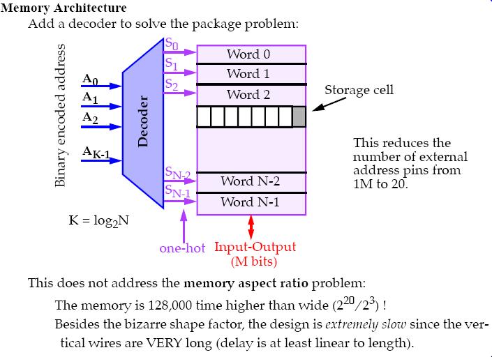
6 Memory architecture [2]
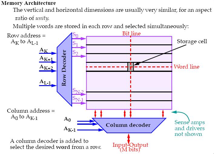
7 Memory architecture [2]
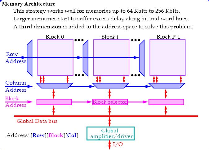
8 Memory architecture [2]

9 ROM/EPROM [2]
10 ROM/EPROM [2]
 [3]")
11 Bus Timing (8086) [3]
![ROM/EPROM [2] Address](/docs-images/87/96491878/images/12-0.jpg "range: FF800h -")
12 ROM/EPROM [2] Address range: FF800h - FFFFFh


 > 8088 mem access")
13 ROM/EPROM 8088, min.mode, EPROM 8 x 2732 = 8 x 4kB = 32 KBytes Address mapping: 0: F8000- F8FFF; 1: F9000- F9FFF;.. 7: FF00-FFFFF EPROM access (450ns) + decoder delay (12ns) > 8088 mem access (460ns) 1 wait state (1 clock = 200ns): total access time =660 ns
14 ROM/EPROM 8088: 8 x 2764 = 8 x 8kB = 64 KB Memory address space: F0000 FFFFF Homework: re-design the adress decoder to map the memory blok in the lower part of the memory space!

15 Address decoders
16 Address decoders
17 Memory connections Parallel connection: extends the memory depth Series connection: extends the memory (word) width
18 Connection to a 16 bit Data Bus (8086, 80286, 80186)
 [1]")
19 RAM Static (SRAM) [1]
20 SRAM [2]
21 SRAM
22 16, 32. bit data bus interface No concern on read operation: memory outputs a whole word (16 bit, 32 bit ) CPU reads the desired byte (BL, BH) or word (Ex: MOV AL, mem ; MOV AH, mem; MOV AX, mem) Only writing must be handled: LWR, HWR Example:
![DRAM Dynamic (DRAM) [1] Size: ½ SRAM cell higher capacity address pins are multiplexed](/docs-images/87/96491878/images/23-1.jpg "Refresh: 1.")
23 DRAM Dynamic (DRAM) [1] Size: ½ SRAM cell higher capacity address pins are multiplexed Refresh: msec special circuit inside DRAM read, write, refresh cycles SDR, DDR, Rambus
24 DRAM [2]
25 DRAM [2] #RAS & #CAS should be provided by a DRAM controller DRAM controller should multiplex (in time) the address lines (ex A0-15) to: row address (ex. A8-15) column address (ex. A0-7)

26 256K X 1 DRAM internal structure [2]
27 DRAM refresh Special refresh cycle - Occurs transparently while other memory components operate and is called transparent refresh or cycle stealing. - A RAS-only cycle strobes a row address into the DRAM, - The capacitors are recharged for the selected row by reading the bits out internally and then writing them back. Example: 256K X 1 DRAM (256 rows x 256 columns x 4 blocks) refresh must occur every 15.6ms (4ms/256). For the 8086, a read or write occurs every 800ns (4x200=4xTclk). 19 memory reads/writes per refresh (15.6ms/0.8ms = 19.5) read/write cycle takes 5% of the refresh time
28 DRAM Controllers [2] address multiplexing and generation of the DRAM control signals. These devices tend to get very complex. We will focus on a simpler device: Intel 82C08, which can control two banks of 256K X 16 DRAM memories for a total of 1 MB. Microprocessor adress A1 through A18 (18 bits) drive the 9 Column Address inputs (AL) and 9 RowAddress inputs (AH) of the 82C08. Either RAS0/CAS0 or RAS1/CAS1 are strobed depending on the address. WE (from the 82C08), BHE and A0 are used to determine if a write is to be performed and which byte(s) (low or high or both) is to be written.
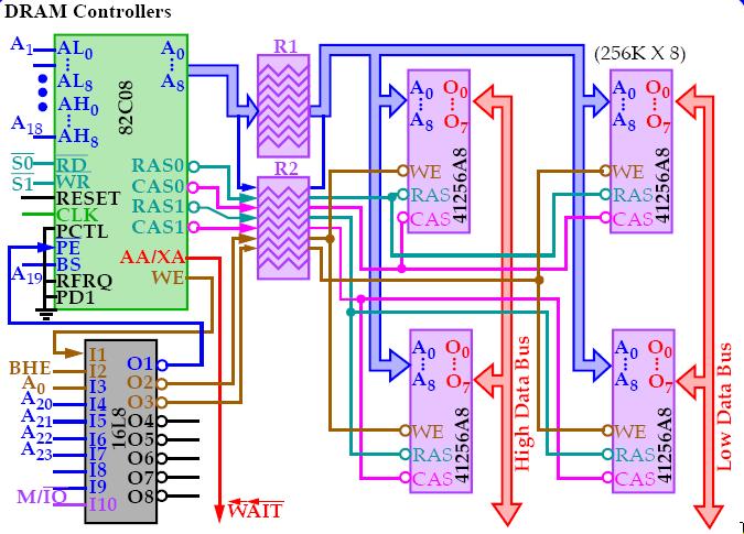
29 DRAM Controllers [2]
30 DRAM Controllers
31 References [1] CSE477, VLSI Digital Circuits, Fall 2005, Lecture 23: Memory Design ROM, SRAM, DRAM, CAM, [2] UMBC, System Design and Programming, Fall 2002, Lecture: Memory 1-3. [3] ELE Microprocessors and Computer Systems, Chapter 8 Memory Address Decoding, [4] Texas Instruments, TMS320C6000 EMIF: Overview of Support of High Performance Memory Technology, Application Report SPRA631 - April 2000 [5] Barry B. Brey, The Intel Microprocessors: 8086/8088, 80186,80286, and Architecture, Programming, and Interfacing, 4-th edition, Prentice Hall, 1996, pp
Design with Microprocessors
 Design with Microprocessors Year III Computer Sci. English 1-st Semester Lecture 12: Memory interfacing Typical Memory Hierarchy [1] On-Chip Components Control edram Datapath RegFile ITLB DTLB Instr Data
CMPEN 411 VLSI Digital Circuits Spring Lecture 22: Memery, ROM
 CMPEN 411 VLSI Digital Circuits Spring 2011 Lecture 22: Memery, ROM [Adapted from Rabaey s Digital Integrated Circuits, Second Edition, 2003 J. Rabaey, A. Chandrakasan, B. Nikolic] Sp11 CMPEN 411 L22 S.1
Microcontroller Systems. ELET 3232 Topic 11: General Memory Interfacing
 Microcontroller Systems ELET 3232 Topic 11: General Memory Interfacing 1 Objectives To become familiar with the concepts of memory expansion and the data and address bus To design embedded systems circuits
Introduction read-only memory random access memory
 Memory Interface Introduction Simple or complex, every microprocessorbased system has a memory system. Almost all systems contain two main types of memory: read-only memory (ROM) and random access memory
Computer Organization. 8th Edition. Chapter 5 Internal Memory
 William Stallings Computer Organization and Architecture 8th Edition Chapter 5 Internal Memory Semiconductor Memory Types Memory Type Category Erasure Write Mechanism Volatility Random-access memory (RAM)
Chapter 5 Internal Memory
 Chapter 5 Internal Memory Memory Type Category Erasure Write Mechanism Volatility Random-access memory (RAM) Read-write memory Electrically, byte-level Electrically Volatile Read-only memory (ROM) Read-only
UMBC D 7 -D. Even bytes 0. 8 bits FFFFFC FFFFFE. location in addition to any 8-bit location. 1 (Mar. 6, 2002) SX 16-bit Memory Interface
 SX 16-bit Memory Interface") 8086-80386SX 16-bit Memory Interface These machines differ from the 8088/80188 in several ways: The data bus is 16-bits wide. The IO/M pin is replaced with M/IO (8086/80186) and MRDC and MWTC for 80286
8086-80386SX 16-bit Memory Interface These machines differ from the 8088/80188 in several ways: The data bus is 16-bits wide. The IO/M pin is replaced with M/IO (8086/80186) and MRDC and MWTC for 80286
Internal Memory. Computer Architecture. Outline. Memory Hierarchy. Semiconductor Memory Types. Copyright 2000 N. AYDIN. All rights reserved.
 Computer Architecture Prof. Dr. Nizamettin AYDIN naydin@yildiz.edu.tr nizamettinaydin@gmail.com Internal Memory http://www.yildiz.edu.tr/~naydin 1 2 Outline Semiconductor main memory Random Access Memory
William Stallings Computer Organization and Architecture 6th Edition. Chapter 5 Internal Memory
 William Stallings Computer Organization and Architecture 6th Edition Chapter 5 Internal Memory Semiconductor Memory Types Semiconductor Memory RAM Misnamed as all semiconductor memory is random access
Organization. 5.1 Semiconductor Main Memory. William Stallings Computer Organization and Architecture 6th Edition
 William Stallings Computer Organization and Architecture 6th Edition Chapter 5 Internal Memory 5.1 Semiconductor Main Memory 5.2 Error Correction 5.3 Advanced DRAM Organization 5.1 Semiconductor Main Memory
Basic Organization Memory Cell Operation. CSCI 4717 Computer Architecture. ROM Uses. Random Access Memory. Semiconductor Memory Types
 CSCI 4717/5717 Computer Architecture Topic: Internal Memory Details Reading: Stallings, Sections 5.1 & 5.3 Basic Organization Memory Cell Operation Represent two stable/semi-stable states representing
Memory and Programmable Logic
 Digital Circuit Design and Language Memory and Programmable Logic Chang, Ik Joon Kyunghee University Memory Classification based on functionality ROM : Read-Only Memory RWM : Read-Write Memory RWM NVRWM
ECE 485/585 Microprocessor System Design
 Microprocessor System Design Lecture 5: Zeshan Chishti DRAM Basics DRAM Evolution SDRAM-based Memory Systems Electrical and Computer Engineering Dept. Maseeh College of Engineering and Computer Science
EE414 Embedded Systems Ch 5. Memory Part 2/2
 EE414 Embedded Systems Ch 5. Memory Part 2/2 Byung Kook Kim School of Electrical Engineering Korea Advanced Institute of Science and Technology Overview 6.1 introduction 6.2 Memory Write Ability and Storage
William Stallings Computer Organization and Architecture 8th Edition. Chapter 5 Internal Memory
 William Stallings Computer Organization and Architecture 8th Edition Chapter 5 Internal Memory Semiconductor Memory The basic element of a semiconductor memory is the memory cell. Although a variety of
Address connections Data connections Selection connections
 Interface (cont..) We have four common types of memory: Read only memory ( ROM ) Flash memory ( EEPROM ) Static Random access memory ( SARAM ) Dynamic Random access memory ( DRAM ). Pin connections common
Large and Fast: Exploiting Memory Hierarchy
 CSE 431: Introduction to Operating Systems Large and Fast: Exploiting Memory Hierarchy Gojko Babić 10/5/018 Memory Hierarchy A computer system contains a hierarchy of storage devices with different costs,
DIGITAL SYSTEM FUNDAMENTALS (ECE421) DIGITAL ELECTRONICS FUNDAMENTAL (ECE422)
 DIGITAL ELECTRONICS FUNDAMENTAL (ECE422)") COURSE / CODE DIGITAL SYSTEM FUNDAMENTALS (ECE421) DIGITAL ELECTRONICS FUNDAMENTAL (ECE422) Memory In computing, memory refers to the computer hardware devices used to store information for immediate use
COURSE / CODE DIGITAL SYSTEM FUNDAMENTALS (ECE421) DIGITAL ELECTRONICS FUNDAMENTAL (ECE422) Memory In computing, memory refers to the computer hardware devices used to store information for immediate use
14:332:331. Week 13 Basics of Cache
 14:332:331 Computer Architecture and Assembly Language Fall 2003 Week 13 Basics of Cache [Adapted from Dave Patterson s UCB CS152 slides and Mary Jane Irwin s PSU CSE331 slides] 331 Lec20.1 Fall 2003 Head
ECE7995 (4) Basics of Memory Hierarchy. [Adapted from Mary Jane Irwin s slides (PSU)]
![ECE7995 (4) Basics of Memory Hierarchy. [Adapted from Mary Jane Irwin s slides (PSU)]](/thumbs/75/72807926.jpg "ECE7995 (4) Basics of Memory Hierarchy. [Adapted from Mary Jane Irwin s slides (PSU)]") ECE7995 (4) Basics of Memory Hierarchy [Adapted from Mary Jane Irwin s slides (PSU)] Major Components of a Computer Processor Devices Control Memory Input Datapath Output Performance Processor-Memory Performance
ECE7995 (4) Basics of Memory Hierarchy [Adapted from Mary Jane Irwin s slides (PSU)] Major Components of a Computer Processor Devices Control Memory Input Datapath Output Performance Processor-Memory Performance
COMP3221: Microprocessors and. and Embedded Systems. Overview. Lecture 23: Memory Systems (I)
") COMP3221: Microprocessors and Embedded Systems Lecture 23: Memory Systems (I) Overview Memory System Hierarchy RAM, ROM, EPROM, EEPROM and FLASH http://www.cse.unsw.edu.au/~cs3221 Lecturer: Hui Wu Session
COMP3221: Microprocessors and Embedded Systems Lecture 23: Memory Systems (I) Overview Memory System Hierarchy RAM, ROM, EPROM, EEPROM and FLASH http://www.cse.unsw.edu.au/~cs3221 Lecturer: Hui Wu Session
INSTITUTO SUPERIOR TÉCNICO. Architectures for Embedded Computing
 UNIVERSIDADE TÉCNICA DE LISBOA INSTITUTO SUPERIOR TÉCNICO Departamento de Engenharia Informática Architectures for Embedded Computing MEIC-A, MEIC-T, MERC Lecture Slides Version 3.0 - English Lecture 16
! Memory Overview. ! ROM Memories. ! RAM Memory " SRAM " DRAM. ! This is done because we can build. " large, slow memories OR
 ESE 57: Digital Integrated Circuits and VLSI Fundamentals Lec 2: April 5, 26 Memory Overview, Memory Core Cells Lecture Outline! Memory Overview! ROM Memories! RAM Memory " SRAM " DRAM 2 Memory Overview
The Memory Hierarchy Part I
 Chapter 6 The Memory Hierarchy Part I The slides of Part I are taken in large part from V. Heuring & H. Jordan, Computer Systems esign and Architecture 1997. 1 Outline: Memory components: RAM memory cells
ECE 485/585 Microprocessor System Design
 Microprocessor System Design Lecture 4: Memory Hierarchy Memory Taxonomy SRAM Basics Memory Organization DRAM Basics Zeshan Chishti Electrical and Computer Engineering Dept Maseeh College of Engineering
Computer Memory. Textbook: Chapter 1
 Computer Memory Textbook: Chapter 1 ARM Cortex-M4 User Guide (Section 2.2 Memory Model) STM32F4xx Technical Reference Manual: Chapter 2 Memory and Bus Architecture Chapter 3 Flash Memory Chapter 36 Flexible
Memory & Simple I/O Interfacing
 Chapter 10 Memory & Simple I/O Interfacing Expected Outcomes Explain the importance of tri-state devices in microprocessor system Distinguish basic type of semiconductor memory and their applications Relate
UMBC. Select. Read. Write. Output/Input-output connection. 1 (Feb. 25, 2002) Four commonly used memories: Address connection ... Dynamic RAM (DRAM)
 Four commonly used memories: Address connection ... Dynamic RAM (DRAM)") Memory Types Two basic types: ROM: Read-only memory RAM: Read-Write memory Four commonly used memories: ROM Flash (EEPROM) Static RAM (SRAM) Dynamic RAM (DRAM) Generic pin configuration: Address connection
Memory Types Two basic types: ROM: Read-only memory RAM: Read-Write memory Four commonly used memories: ROM Flash (EEPROM) Static RAM (SRAM) Dynamic RAM (DRAM) Generic pin configuration: Address connection
Contents. Memory System Overview Cache Memory. Internal Memory. Virtual Memory. Memory Hierarchy. Registers In CPU Internal or Main memory
 Memory Hierarchy Contents Memory System Overview Cache Memory Internal Memory External Memory Virtual Memory Memory Hierarchy Registers In CPU Internal or Main memory Cache RAM External memory Backing
Chapter 4 Main Memory
 Chapter 4 Main Memory Course Outcome (CO) - CO2 Describe the architecture and organization of computer systems Program Outcome (PO) PO1 Apply knowledge of mathematics, science and engineering fundamentals
Basics DRAM ORGANIZATION. Storage element (capacitor) Data In/Out Buffers. Word Line. Bit Line. Switching element HIGH-SPEED MEMORY SYSTEMS
 Data In/Out Buffers. Word Line. Bit Line. Switching element HIGH-SPEED MEMORY SYSTEMS") Basics DRAM ORGANIZATION DRAM Word Line Bit Line Storage element (capacitor) In/Out Buffers Decoder Sense Amps... Bit Lines... Switching element Decoder... Word Lines... Memory Array Page 1 Basics BUS
Basics DRAM ORGANIZATION DRAM Word Line Bit Line Storage element (capacitor) In/Out Buffers Decoder Sense Amps... Bit Lines... Switching element Decoder... Word Lines... Memory Array Page 1 Basics BUS
ORG ; Week8. Memory and Memory Interfacing
 Dec 10 Hex A Bin 00001010 ORG ; Week8 Memory and Memory Interfacing OBJECTIVES this chapter enables the student to: Define the terms capacity, organization, and speed as used in semiconductor memories.
Semiconductor Memory Classification. Today. ESE 570: Digital Integrated Circuits and VLSI Fundamentals. CPU Memory Hierarchy.
 ESE 57: Digital Integrated Circuits and VLSI Fundamentals Lec : April 4, 7 Memory Overview, Memory Core Cells Today! Memory " Classification " ROM Memories " RAM Memory " Architecture " Memory core " SRAM
Concept of Memory. The memory of computer is broadly categories into two categories:
 Concept of Memory We have already mentioned that digital computer works on stored programmed concept introduced by Von Neumann. We use memory to store the information, which includes both program and data.
COSC 6385 Computer Architecture - Memory Hierarchies (III)
") COSC 6385 Computer Architecture - Memory Hierarchies (III) Edgar Gabriel Spring 2014 Memory Technology Performance metrics Latency problems handled through caches Bandwidth main concern for main memory
COSC 6385 Computer Architecture - Memory Hierarchies (III) Edgar Gabriel Spring 2014 Memory Technology Performance metrics Latency problems handled through caches Bandwidth main concern for main memory
Computer System Components
 Computer System Components CPU Core 1 GHz - 3.2 GHz 4-way Superscaler RISC or RISC-core (x86): Deep Instruction Pipelines Dynamic scheduling Multiple FP, integer FUs Dynamic branch prediction Hardware
Memory Interfacing & decoding. Intel CPU s
 Memory Interfacing & decoding in Intel CPU s Outline Address decoding Chip select Memory configurations Minimum Mode - - A19 - A19 - Simplified Drawing of 8088 Minimum Mode MEMORY MEMW When Memory is selected?
CENG3420 Lecture 08: Memory Organization
 CENG3420 Lecture 08: Memory Organization Bei Yu byu@cse.cuhk.edu.hk (Latest update: February 22, 2018) Spring 2018 1 / 48 Overview Introduction Random Access Memory (RAM) Interleaving Secondary Memory
Embedded Systems Design: A Unified Hardware/Software Introduction. Outline. Chapter 5 Memory. Introduction. Memory: basic concepts
 Hardware/Software Introduction Chapter 5 Memory Outline Memory Write Ability and Storage Permanence Common Memory Types Composing Memory Memory Hierarchy and Cache Advanced RAM 1 2 Introduction Memory:
Embedded Systems Design: A Unified Hardware/Software Introduction. Chapter 5 Memory. Outline. Introduction
 Hardware/Software Introduction Chapter 5 Memory 1 Outline Memory Write Ability and Storage Permanence Common Memory Types Composing Memory Memory Hierarchy and Cache Advanced RAM 2 Introduction Embedded
Chapter 5. Internal Memory. Yonsei University
 Chapter 5 Internal Memory Contents Main Memory Error Correction Advanced DRAM Organization 5-2 Memory Types Memory Type Category Erasure Write Mechanism Volatility Random-access memory(ram) Read-write
Memory latency: Affects cache miss penalty. Measured by:
 Main Memory Main memory generally utilizes Dynamic RAM (DRAM), which use a single transistor to store a bit, but require a periodic data refresh by reading every row. Static RAM may be used for main memory
Power Reduction Techniques in the Memory System. Typical Memory Hierarchy
 Power Reduction Techniques in the Memory System Low Power Design for SoCs ASIC Tutorial Memories.1 Typical Memory Hierarchy On-Chip Components Control edram Datapath RegFile ITLB DTLB Instr Data Cache
ECSE-2610 Computer Components & Operations (COCO)
") ECSE-2610 Computer Components & Operations (COCO) Part 18: Random Access Memory 1 Read-Only Memories 2 Why ROM? Program storage Boot ROM for personal computers Complete application storage for embedded
ECSE-2610 Computer Components & Operations (COCO) Part 18: Random Access Memory 1 Read-Only Memories 2 Why ROM? Program storage Boot ROM for personal computers Complete application storage for embedded
CS 320 February 2, 2018 Ch 5 Memory
 CS 320 February 2, 2018 Ch 5 Memory Main memory often referred to as core by the older generation because core memory was a mainstay of computers until the advent of cheap semi-conductor memory in the
(Advanced) Computer Organization & Architechture. Prof. Dr. Hasan Hüseyin BALIK (5 th Week)
 Computer Organization & Architechture. Prof. Dr. Hasan Hüseyin BALIK (5 th Week)") + (Advanced) Computer Organization & Architechture Prof. Dr. Hasan Hüseyin BALIK (5 th Week) + Outline 2. The computer system 2.1 A Top-Level View of Computer Function and Interconnection 2.2 Cache Memory
+ (Advanced) Computer Organization & Architechture Prof. Dr. Hasan Hüseyin BALIK (5 th Week) + Outline 2. The computer system 2.1 A Top-Level View of Computer Function and Interconnection 2.2 Cache Memory
7/6/2011. Introduction. Chapter Objectives Upon completion of this chapter, you will be able to:
 Introduction Simple or complex, every microprocessorbased system has a memory system. Almost all systems contain two main types of memory: read-only memory (ROM) and random access memory (RAM) or read/write
ELEC 5200/6200 Computer Architecture and Design Spring 2017 Lecture 7: Memory Organization Part II
 ELEC 5200/6200 Computer Architecture and Design Spring 2017 Lecture 7: Organization Part II Ujjwal Guin, Assistant Professor Department of Electrical and Computer Engineering Auburn University, Auburn,
Read and Write Cycles
 Read and Write Cycles The read cycle is shown. Figure 41.1a. The RAS and CAS signals are activated one after the other to latch the multiplexed row and column addresses respectively applied at the multiplexed
Mainstream Computer System Components CPU Core 2 GHz GHz 4-way Superscaler (RISC or RISC-core (x86): Dynamic scheduling, Hardware speculation
: Dynamic scheduling, Hardware speculation") Mainstream Computer System Components CPU Core 2 GHz - 3.0 GHz 4-way Superscaler (RISC or RISC-core (x86): Dynamic scheduling, Hardware speculation One core or multi-core (2-4) per chip Multiple FP, integer
Mainstream Computer System Components CPU Core 2 GHz - 3.0 GHz 4-way Superscaler (RISC or RISC-core (x86): Dynamic scheduling, Hardware speculation One core or multi-core (2-4) per chip Multiple FP, integer
Memory Pearson Education, Inc., Hoboken, NJ. All rights reserved.
 1 Memory + 2 Location Internal (e.g. processor registers, cache, main memory) External (e.g. optical disks, magnetic disks, tapes) Capacity Number of words Number of bytes Unit of Transfer Word Block Access
CS650 Computer Architecture. Lecture 9 Memory Hierarchy - Main Memory
 CS65 Computer Architecture Lecture 9 Memory Hierarchy - Main Memory Andrew Sohn Computer Science Department New Jersey Institute of Technology Lecture 9: Main Memory 9-/ /6/ A. Sohn Memory Cycle Time 5
Memory Overview. Overview - Memory Types 2/17/16. Curtis Nelson Walla Walla University
 Memory Overview Curtis Nelson Walla Walla University Overview - Memory Types n n n Magnetic tape (used primarily for long term archive) Magnetic disk n Hard disk (File, Directory, Folder) n Floppy disks
CENG 3420 Computer Organization and Design. Lecture 08: Cache Review. Bei Yu
 CENG 3420 Computer Organization and Design Lecture 08: Cache Review Bei Yu CEG3420 L08.1 Spring 2016 A Typical Memory Hierarchy q Take advantage of the principle of locality to present the user with as
Integrated Circuits & Systems
 Federal University of Santa Catarina Center for Technology Computer Science & Electronics Engineering Integrated Circuits & Systems INE 5442 Lecture 23-1 guntzel@inf.ufsc.br Semiconductor Memory Classification
eaymanelshenawy.wordpress.com
 Lectures on Memory Interface Designed and Presented by Dr. Ayman Elshenawy Elsefy Dept. of Systems & Computer Eng.. Al-Azhar University Email : eaymanelshenawy@yahoo.com eaymanelshenawy.wordpress.com Lecture
Magnetic core memory (1951) cm 2 ( bit)
 cm 2 ( bit)") Magnetic core memory (1951) 16 16 cm 2 (128 128 bit) Semiconductor Memory Classification Read-Write Memory Non-Volatile Read-Write Memory Read-Only Memory Random Access Non-Random Access EPROM E 2 PROM
Magnetic core memory (1951) 16 16 cm 2 (128 128 bit) Semiconductor Memory Classification Read-Write Memory Non-Volatile Read-Write Memory Read-Only Memory Random Access Non-Random Access EPROM E 2 PROM
Computer Organization and Assembly Language (CS-506)
") Computer Organization and Assembly Language (CS-506) Muhammad Zeeshan Haider Ali Lecturer ISP. Multan ali.zeeshan04@gmail.com https://zeeshanaliatisp.wordpress.com/ Lecture 2 Memory Organization and Structure
Computer Organization and Assembly Language (CS-506) Muhammad Zeeshan Haider Ali Lecturer ISP. Multan ali.zeeshan04@gmail.com https://zeeshanaliatisp.wordpress.com/ Lecture 2 Memory Organization and Structure
CS 265. Computer Architecture. Wei Lu, Ph.D., P.Eng.
 CS 265 Computer Architecture Wei Lu, Ph.D., P.Eng. Part 4: Memory Organization Our goal: understand the basic types of memory in computer understand memory hierarchy and the general process to access memory
Memory latency: Affects cache miss penalty. Measured by:
 Main Memory Main memory generally utilizes Dynamic RAM (DRAM), which use a single transistor to store a bit, but require a periodic data refresh by reading every row. Static RAM may be used for main memory
Summer 2003 Lecture 18 07/09/03
 Summer 2003 Lecture 18 07/09/03 NEW HOMEWORK Instruction Execution Times: The 8088 CPU is a synchronous machine that operates at a particular clock frequency. In the case of the original IBM PC, that clock
Memory classification:- Topics covered:- types,organization and working
 Memory classification:- Topics covered:- types,organization and working 1 Contents What is Memory? Cache Memory PC Memory Organisation Types 2 Memory what is it? Usually we consider this to be RAM, ROM
Main Memory. EECC551 - Shaaban. Memory latency: Affects cache miss penalty. Measured by:
 Main Memory Main memory generally utilizes Dynamic RAM (DRAM), which use a single transistor to store a bit, but require a periodic data refresh by reading every row (~every 8 msec). Static RAM may be
Module 5a: Introduction To Memory System (MAIN MEMORY)
") Module 5a: Introduction To Memory System (MAIN MEMORY) R E F E R E N C E S : S T A L L I N G S, C O M P U T E R O R G A N I Z A T I O N A N D A R C H I T E C T U R E M O R R I S M A N O, C O M P U T E
Module 5a: Introduction To Memory System (MAIN MEMORY) R E F E R E N C E S : S T A L L I N G S, C O M P U T E R O R G A N I Z A T I O N A N D A R C H I T E C T U R E M O R R I S M A N O, C O M P U T E
CS 261 Fall Mike Lam, Professor. Memory
 CS 261 Fall 2016 Mike Lam, Professor Memory Topics Memory hierarchy overview Storage technologies SRAM DRAM PROM / flash Disk storage Tape and network storage I/O architecture Storage trends Latency comparisons
Mainstream Computer System Components
 Mainstream Computer System Components Double Date Rate (DDR) SDRAM One channel = 8 bytes = 64 bits wide Current DDR3 SDRAM Example: PC3-12800 (DDR3-1600) 200 MHz (internal base chip clock) 8-way interleaved
EECS150 - Digital Design Lecture 16 Memory 1
 EECS150 - Digital Design Lecture 16 Memory 1 March 13, 2003 John Wawrzynek Spring 2003 EECS150 - Lec16-mem1 Page 1 Memory Basics Uses: Whenever a large collection of state elements is required. data &
COMPUTER ARCHITECTURES
 COMPUTER ARCHITECTURES Random Access Memory Technologies Gábor Horváth BUTE Department of Networked Systems and Services ghorvath@hit.bme.hu Budapest, 2019. 02. 24. Department of Networked Systems and
CPSC 352. Chapter 7: Memory. Computer Organization. Principles of Computer Architecture by M. Murdocca and V. Heuring
 7- CPSC 352 Computer Organization 7-2 Chapter Contents 7. The Memory Hierarchy 7.2 Random Access Memory 7.3 Chip Organization 7.4 Commercial Memory Modules 7.5 Read-Only Memory 7.6 Cache Memory 7.7 Virtual
UNIT V (PROGRAMMABLE LOGIC DEVICES)
") UNIT V (PROGRAMMABLE LOGIC DEVICES) Introduction There are two types of memories that are used in digital systems: Random-access memory(ram): perform both the write and read operations. Read-only memory(rom):
UNIT V (PROGRAMMABLE LOGIC DEVICES) Introduction There are two types of memories that are used in digital systems: Random-access memory(ram): perform both the write and read operations. Read-only memory(rom):
CSE 431 Computer Architecture Fall Chapter 5A: Exploiting the Memory Hierarchy, Part 1
 CSE 431 Computer Architecture Fall 2008 Chapter 5A: Exploiting the Memory Hierarchy, Part 1 Mary Jane Irwin ( www.cse.psu.edu/~mji ) [Adapted from Computer Organization and Design, 4 th Edition, Patterson
CS429: Computer Organization and Architecture
 CS429: Computer Organization and Architecture Dr. Bill Young Department of Computer Sciences University of Texas at Austin Last updated: April 9, 2018 at 12:16 CS429 Slideset 17: 1 Random-Access Memory
Allmost all systems contain two main types of memory :
 Memory Interface Allmost all systems contain two main types of memory : read-only memory (ROM) system software and permanent system data random access memory (RAM) or read/write memory application software
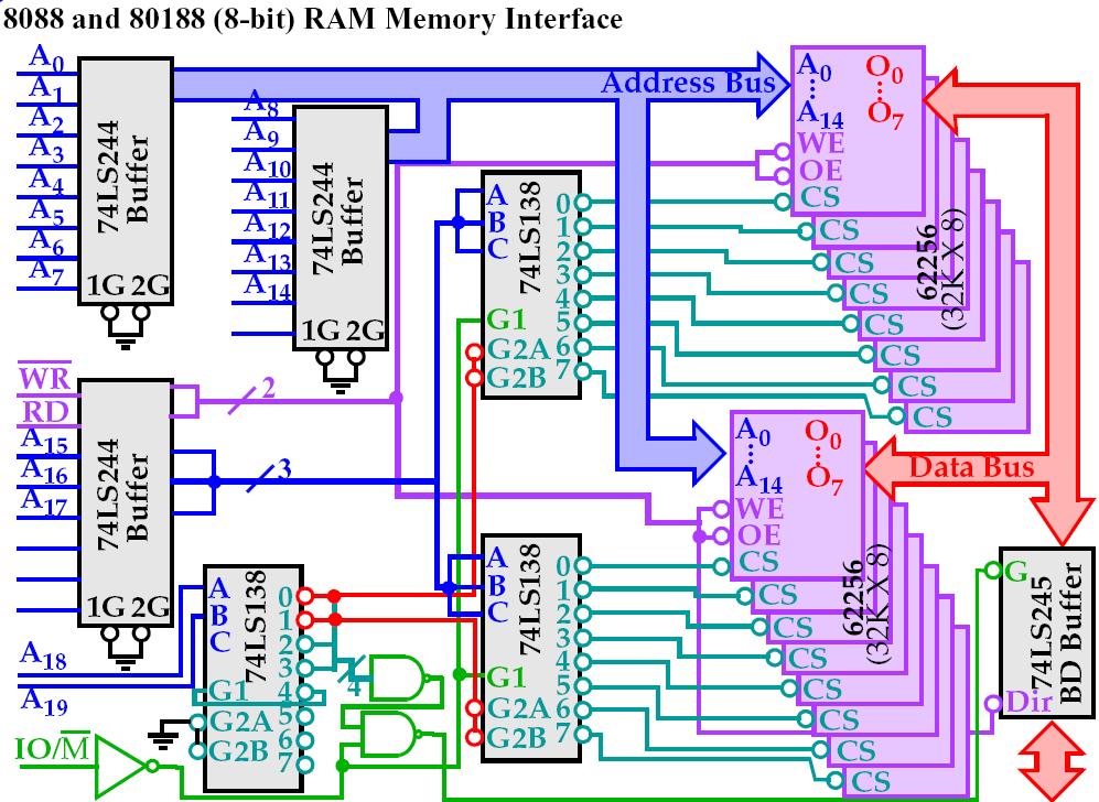
FIGURE Three EPROMs interfaced to the 8088 microprocessor.
 10 3 8088 AND 80188 (8-BIT) MEMORY INTERFACE: Basic 8088/80188 Memory Interface: The 8088 and 80188 microprocessors have an 8-bit data bus. The memory system must decode the address to select a memory
ELCT 912: Advanced Embedded Systems
 Advanced Embedded Systems Lecture 2: Memory and Programmable Logic Dr. Mohamed Abd El Ghany, Memory Random Access Memory (RAM) Can be read and written Static Random Access Memory (SRAM) Data stored so
Chapter 5B. Large and Fast: Exploiting Memory Hierarchy
 Chapter 5B Large and Fast: Exploiting Memory Hierarchy One Transistor Dynamic RAM 1-T DRAM Cell word access transistor V REF TiN top electrode (V REF ) Ta 2 O 5 dielectric bit Storage capacitor (FET gate,
CENG4480 Lecture 09: Memory 1
 CENG4480 Lecture 09: Memory 1 Bei Yu byu@cse.cuhk.edu.hk (Latest update: November 8, 2017) Fall 2017 1 / 37 Overview Introduction Memory Principle Random Access Memory (RAM) Non-Volatile Memory Conclusion
ESE370: Circuit-Level Modeling, Design, and Optimization for Digital Systems
 ESE370: Circuit-Level Modeling, Design, and Optimization for Digital Systems Lec 26: November 9, 2018 Memory Overview Dynamic OR4! Precharge time?! Driving input " With R 0 /2 inverter! Driving inverter
EECS150 - Digital Design Lecture 16 - Memory
 EECS150 - Digital Design Lecture 16 - Memory October 17, 2002 John Wawrzynek Fall 2002 EECS150 - Lec16-mem1 Page 1 Memory Basics Uses: data & program storage general purpose registers buffering table lookups
ENGIN 112 Intro to Electrical and Computer Engineering
 ENGIN 112 Intro to Electrical and Computer Engineering Lecture 30 Random Access Memory (RAM) Overview Memory is a collection of storage cells with associated input and output circuitry Possible to read
Memory Challenges. Issues & challenges in memory design: Cost Performance Power Scalability
 Memory Devices 1 Memory Challenges Issues & challenges in memory design: Cost Performance Power Scalability 2 Memory - Overview Definitions: RAM random access memory DRAM dynamic RAM SRAM static RAM Volatile
CS429: Computer Organization and Architecture
 CS429: Computer Organization and Architecture Dr. Bill Young Department of Computer Sciences University of Texas at Austin Last updated: November 28, 2017 at 14:31 CS429 Slideset 18: 1 Random-Access Memory
Memory. Memory Technologies
 Memory Memory technologies Memory hierarchy Cache basics Cache variations Virtual memory Synchronization Galen Sasaki EE 36 University of Hawaii Memory Technologies Read Only Memory (ROM) Static RAM (SRAM)
Transistor: Digital Building Blocks
 Final Exam Review Transistor: Digital Building Blocks Logically, each transistor acts as a switch Combined to implement logic functions (gates) AND, OR, NOT Combined to build higher-level structures Multiplexer,
Menu. word size # of words byte = 8 bits
 Menu LSI Components >Random Access Memory (RAM) Static RAM (SRAM) Dynamic RAM (DRAM) Read-Only Memory (ROM) Look into my... See figures from Lam text on web: RAM_ROM_ch6.pdf 1 It can be thought of as 1
Memory. Lecture 22 CS301
 Memory Lecture 22 CS301 Administrative Daily Review of today s lecture w Due tomorrow (11/13) at 8am HW #8 due today at 5pm Program #2 due Friday, 11/16 at 11:59pm Test #2 Wednesday Pipelined Machine Fetch
8051 INTERFACING TO EXTERNAL MEMORY
 8051 INTERFACING TO EXTERNAL MEMORY Memory Capacity The number of bits that a semiconductor memory chip can store Called chip capacity It can be in units of Kbits (kilobits), Mbits (megabits), and so on
CMSC 313 COMPUTER ORGANIZATION & ASSEMBLY LANGUAGE PROGRAMMING LECTURE 26, SPRING 2013
 CMSC 313 COMPUTER ORGANIZATION & ASSEMBLY LANGUAGE PROGRAMMING LECTURE 26, SPRING 2013 TOPICS TODAY End of the Semester Stuff Homework 5 Memory Hierarchy Storage Technologies (RAM & Disk) Caching END OF
Contents. Main Memory Memory access time Memory cycle time. Types of Memory Unit RAM ROM
 Memory Organization Contents Main Memory Memory access time Memory cycle time Types of Memory Unit RAM ROM Memory System Virtual Memory Cache Memory - Associative mapping Direct mapping Set-associative
ELE 758 * DIGITAL SYSTEMS ENGINEERING * MIDTERM TEST * Circle the memory type based on electrically re-chargeable elements
 ELE 758 * DIGITAL SYSTEMS ENGINEERING * MIDTERM TEST * Student name: Date: Example 1 Section: Memory hierarchy (SRAM, DRAM) Question # 1.1 Circle the memory type based on electrically re-chargeable elements
Chapter TEN. Memory and Memory Interfacing
 Chapter TEN Memory and Memory Interfacing OBJECTIVES this chapter enables the student to: Define the terms capacity, organization, and speed as used in semiconductor memories. Calculate the chip capacity
Structure of Computer Systems
 222 Structure of Computer Systems Figure 4.64 shows how a page directory can be used to map linear addresses to 4-MB pages. The entries in the page directory point to page tables, and the entries in a
CHAPTER TWELVE - Memory Devices
 CHAPTER TWELVE - Memory Devices 12.1 6x1,024 = 16,384 words; 32 bits/word; 16,384x32 = 524,288 cells 12.2 16,384 addresses; one per word. 12.3 2 16 = 65,536 words = 64K. Thus, memory capacity is 64Kx4.
Mainstream Computer System Components
 Mainstream Computer System Components Double Date Rate (DDR) SDRAM One channel = 8 bytes = 64 bits wide Current DDR3 SDRAM Example: PC3-2800 (DDR3-600) 200 MHz (internal base chip clock) 8-way interleaved
MEMORY SYSTEM MEMORY TECHNOLOGY SUMMARY DESIGNING MEMORY SYSTEM. The goal in designing any memory system is to provide
 SUMMARY MEMORY SYSTEM ORGANIZATION Memory technology Hierarchical memory systems Characteristics of the storage-device Main memory organization SRAM DRAM Cache memory COMPUTER ARCHITECTURE 2 MEMORY TECHNOLOGY
Interface DAC to a PC. Control Word of MC1480 DAC (or DAC 808) 8255 Design Example. Engineering 4862 Microprocessors
 8255 Design Example. Engineering 4862 Microprocessors") Interface DAC to a PC Engineering 4862 Microprocessors Lecture 22 Cheng Li EN-4012 licheng@engr.mun.ca DAC (Digital-to-Analog Converter) Device used to convert digital pulses to analog signals Two methods
Interface DAC to a PC Engineering 4862 Microprocessors Lecture 22 Cheng Li EN-4012 licheng@engr.mun.ca DAC (Digital-to-Analog Converter) Device used to convert digital pulses to analog signals Two methods
Computer Memory Basic Concepts. Lecture for CPSC 5155 Edward Bosworth, Ph.D. Computer Science Department Columbus State University
 Computer Memory Basic Concepts Lecture for CPSC 5155 Edward Bosworth, Ph.D. Computer Science Department Columbus State University The Memory Component The memory stores the instructions and data for an
Foundations of Computer Systems
 18-600 Foundations of Computer Systems Lecture 12: The Memory Hierarchy John Shen & Zhiyi Yu October 10, 2016 Required Reading Assignment: Chapter 6 of CS:APP (3 rd edition) by Randy Bryant & Dave O Hallaron
Lecture 13: Memory and Programmable Logic
 Lecture 13: Memory and Programmable Logic Syed M. Mahmud, Ph.D ECE Department Wayne State University Aby K George, ECE Department, Wayne State University Contents Introduction Random Access Memory Memory
Chapter 8 Memory Basics
 Logic and Computer Design Fundamentals Chapter 8 Memory Basics Charles Kime & Thomas Kaminski 2008 Pearson Education, Inc. (Hyperlinks are active in View Show mode) Overview Memory definitions Random Access