Q.2 a. What are basic operational concepts? Explain. (6)
|
|
|
- Arlene Morton
- 5 years ago
- Views:
Transcription
1 Q.2 a. What are basic operational concepts? Explain. (6) Basic operational concepts-to perform a given task an appropriate program consisting of a list of instructions is stored in the memory. Individual instructions are brought from the memory into the processor, which executes the specified operations. Data to be stored are also stored in the memory. Examples: - Add LOCA, R0 This instruction adds the operand at memory location LOCA, to operand in register R0 & places the sum into register. This instruction requires the performance of several steps, 1. First the instruction is fetched from the memory into the processor. 2. The operand at LOCA is fetched and added to the contents of R0 3. Finally the resulting sum is stored in the register R0 The preceding add instruction combines a memory access operation with an ALU Operations. In some other type of computers, these two types of operations are performed by separate instructions for performance reasons. Load LOCA, R1 Add R1, R0 Transfers between the memory and the processor are started by sending the address of the memory location to be accessed to the memory unit and issuing the appropriate control signals. The data are then transferred to or from the memory. The instruction register (IR):- Holds the instructions that is currently being executed. Its output is available for the control circuits which generates the timing signals that control the various processing elements in one execution of instruction. The program counter PC:- This is another specialized register that keeps track of execution of a program. It contains the memory address of the next instruction to be fetched and executed The other two registers which facilitate communication with memory are: - 1. MAR (Memory Address Register):- It holds the address of the location to be accessed. 2. MDR (Memory Data Register):- It contains the data to be written into or read out of the address location. Operating steps are 1. Programs reside in the memory & usually get these through the I/P unit. 2. Execution of the program starts when the PC is set to point at the first instruction of the program. 3. Contents of PC are transferred to MAR and a Read Control Signal is sent to the memory. 4. After the time required to access the memory elapses, the address word is read out of the memory and loaded into the MDR. 5. Now contents of MDR are transferred to the IR & now the instruction is ready to be decoded and executed. 6. If the instruction involves an operation by the ALU, it is necessary to obtain the required operands. 7. An operand in the memory is fetched by sending its address to MAR & Initiating a read cycle. 8. When the operand has been read from the memory to the MDR, it is transferred from MDR to the ALU. 9. After one or two such repeated cycles, the ALU can perform the desired operation. 10. If the result of this operation is to be stored in the memory, the result is sent to MDR. 11. Address of location where the result is stored is sent to MAR & a write cycle is initiated. 12. The contents of PC are incremented so that PC points to the next instruction that is to be executed. Normal execution of a program may be preempted (temporarily interrupted) if some devices require urgent servicing, to do this one device raises an Interrupt signal. An interrupt is a request signal from an I/O device for service by the processor. The processor provides the requested service by executing an appropriate interrupt service routine. The Diversion may change the internal stage of the processor its state must be saved in the memory location before interruption. When the interrupt-routine service is completed the state of the processor is restored so that the interrupted program may continue.

2 b. Explain single bus structure. (5) Bus structure - The simplest and most common way of interconnecting various parts of the computer. To achieve a reasonable speed of operation, a computer must be organized so that all its units can handle one full word of data at a given time. A group of lines that serve as a connecting port for several devices is called a bus. In addition to the lines that carry the data, the bus must have lines for address and control purpose. Simplest way to interconnect is to use the single bus as shown. Since the bus can be used for only one transfer at a time, only two units can actively use the bus at any given time. Bus control lines are used to arbitrate multiple requests for use of one bus. Single bus structure is Low cost Very flexible for attaching peripheral devices Multiple bus structure certainly increases, the performance but also increases the cost significantly.
3 c. Explain register transfer notation (RTN). (5) REGISTER TRANSFER NOTATION:-Transfer of information from one location in the computer to another. Possible locations that may be involved in such transfers are memory locations that may be involved in such transfers are memory locations, processor registers, or registers in the I/O subsystem. Most of the time, we identify a location by a symbolic name standing for its hardware binary address. Example, names for the addresses of memory locations may be LOC, PLACE, A, VAR2; processor registers names may be R0, R5; and I/O register names may be DATAIN, OUTSTATUS, and so on. The contents of a location are denoted by placing square brackets around the name of the location. Thus, the expression R1 [LOC] Means that the contents of memory location LOC are transferred into processor register R1. As another example, consider the operation that adds the contents of registers R1 and R2, and then places their sum into register R3. This action is indicated as R3 [R1] + [R2] This type of notation is known as Register Transfer Notation (RTN). Note that the right-hand side of an RTN expression always denotes a value, and the left-hand side is the name of a location where the value is to be places, overwriting the old contents of that location. Q.3 a. Define addressing mode. Explain different types of addressing modes. (2+6) Addressing modes:in general, a program operates on data that reside in the computer s memory. These data can be organized in a variety of ways. If we want to keep track of students names, we can write them in a list. Programmers use organizations called data structures to represent the data used in computations. These include lists, linked lists, arrays, queues, and so on. Programs are normally written in a high-level language, which enables the programmer to use constants, local and global variables, pointers, and arrays. The different ways in which the location of an operand is specified in an instruction are referred to as addressing modes. Types of addressing mode- Register mode - The operand is the contents of a processor register; the name (address) of the register is given in the instruction. Absolute mode The operand is in a memory location; the address of this location is given explicitly in the instruction. (In some assembly languages, this mode is called Direct). The instruction Move LOC, R2 Processor registers are used as temporary storage locations where the data is a register are accessed using the Register mode. The Absolute mode can represent global variables in a program. A declaration such as Integer A, B; Immediate mode The operand is given explicitly in the instruction. For example, the instruction Move 200immediate, R0 Places the value 200 in register R0. Clearly, the Immediate mode is only used to specify the value of a source operand. Using a subscript to denote the Immediate mode is not appropriate in assembly languages. A common convention is to use the sharp sign (#) in front of the value to indicate that this value is to be used as an immediate operand. Hence, we write the instruction above in the form INDIRECTION AND POINTERS:- In the addressing modes that follow, the instruction does not give the operand or its address explicitly, Instead, it provides information from which the memory address of the operand can be determined. We refer to this address as the effective address (EA) of IETE 3
4 the operand. Indirect mode The effective address of the operand is the contents of a register or memory location whose address appears in the instruction ove #200, R0 To execute the Add instruction in fig (a), the processor uses the value which is in register R1, as the effective address of the operand. It requests a read operation from the memory to read the contents of location B. the value read is the desired operand, which the processor adds to the contents of register R0. Indirect addressing through a memory location is also possible as shown in fig (b). In this case, the processor first reads the contents of memory location A, then requests a second read operation using the value B as an address to obtain the operand INDEXING AND ARRAYS:- A different kind of flexibility for accessing operands is useful in dealing with lists and arrays. Index mode the effective address of the operand is generated by adding a constant value to the contents of a register. The register use may be either a special register provided for this purpose, or, more commonly, it may be any one of a set of general-purpose registers in the processor. In either case, it is referred to as index register. We indicate the Index mode symbolically as X (Ri) Where X denotes the constant value contained in the instruction and Ri is the name of the register involved. The effective address of the operand is given by EA = X + [Rj] The contents of the index register are not changed in the process of generating the effective address. In an assembly language program, the constant X may be given either as an explicit number or as a symbolic name representing a numerical value. RELATIVE ADDRESSING:-We have defined the Index mode using general-purpose processor registers. A useful version of this mode is obtained if the program counter, PC, is used instead of a general purpose register. Then, X(PC) can be used to address a memory location that is X bytes away from the location presently pointed to by the program counter. Relative mode The effective address is determined by the Index mode using the program counter in place of the general-purpose register Ri. This mode can be used to access data operands. But, its most common use is to specify the target address in branch instructions. An instruction such asbranch > 0 LOOP Causes program execution to go to the branch target location identified by the name LOOP if the branch condition is satisfied. This location can be computed by specifying it as an offset from the current value of the program counter. Since the branch target may be either before or after the branch instruction, the offset is given as a signednumber. Autoincrement mode the effective address of the operand is the contents of a register specified in the instruction. After accessing the operand, the contents of this register are automatically to point to the next item in a list. (Ri)+ Autodecrement mode the contents of a register specified in the instruction are first automatically decremented and are then used as the effective address of the operand b. Define stack. Explain types of instruction format. (2+6) Stack - A computer program often needs to perform a particular subtask using the familiar subroutine structure. In order to organize the control and information linkage between the main program and the subroutine, a data structure called a stack is used. Data operated on by a program can be organized in a variety of ways. We have already encountered data structured as IETE 4
5 lists. Now, we consider an important data structure known as a stack. A stack is a list of data elements, usually words or bytes, with the accessing restriction that elements can be added or removed at one end of the list only. This end is called the top of the stack, and the other end is called the bottom. Another descriptive phrase, last-in-first-out (LIFO) stack, is also used to describe this type of storage mechanism; the last data item placed on the stack is the first one removed when retrieval begins. The terms push and pop are used to describe placing a new item on the stack and removing the top item from the stack, respectively. Instruction Format:-We have seen instructions that perform operations such as add, subtract, move, shift, rotate, and branch. These instructions may use operands of different sizes, such as 32- bit and 8-bit numbers or 8-bit ASCII-encoded characters. The type of operation that is to be performed and the type of operands used may be specified using an encoded binary pattern referred to as the OP code for the given instruction. Suppose that 8 bits are allocated for this purpose, giving 256 possibilities for specifying different instructions. This leaves 24 bits to specify the rest of the required information Let us examine some typical cases. The instruction Add R1, R2 Has to specify the registers R1 and R2, in addition to the OP code. If the processor has 16 registers, then four bits are needed to identify each register. Additional bits are needed to indicate that the Register addressing mode is used for each operand. The instruction Move 24(R0), R5 (a) One-word instruction Opcode Source Destination Other info (b) Two-Word instruction opcode Source Destination Other info Memory address/immediate operand (c) Three-operand instruction Op code Ri Rj Rk Other info Requires 18 bits to denote the OP code, the addressing modes, and the register. This leaves 14 bits to express the address that corresponds to LOC, which is clearly insufficient. And #$FF R2 In which case the second word gives a full 32-bit immediate operand. If we want to allow an instruction in which two operands can be specified using the Absolute addressing mode, for example Move LOC1, LOC2 Then it becomes necessary to use tow additional words for the 32-bit addresses of the operands. This approach results in instructions of variable length, dependent on the number of operands and the type of addressing modes used. Using multiple words, we can implement quite complex instructions, closely resembling operations in high-level programming languages. The term complex instruction set computer (CISC) has been used to refer to processors that use instruction sets of this type. The restriction that an instruction must occupy only one word has led to a style of computers that have become known as reduced instruction set computer (RISC). The RISC approach introduced other restrictions, such as that all manipulation of data must be done on operands that are already in processor registers. This restriction means that the above addition would need a two-instruction sequence Move (R3), R1 IETE 5
6 Add R1, R2 If the Add instruction only has to specify the two registers, it will need just a portion of a 32-bit word. So, we may provide a more powerful instruction that uses three operands Add R1, R2, R3 Which performs the operation R3 [R1] + [R2] A possible format for such an instruction in shown in fig c. Of course, the processor has to be able to deal with such three-operand instructions. In an instruction set where all arithmetic and logical operations use only register operands, the only memory references are made to load/store the operands into/from the processor registers. RISC-type instruction sets typically have fewer and less complex instructions than CISC-type. Q.4 a. Explain synchronous bus and asynchronous bus. (8) Synchronous Bus:-In a synchronous bus, all devices derive timing information from a common clock line. Equally spaced pulses on this line define equal time intervals. In the simplest form of a synchronous bus, each of these intervals constitutes a bus cycle during which one data transfer can take place. Such a scheme is illustrated in figure 7 The address and data lines in this and subsequent figures are shown as high and low at the same time. This is a common convention indicating that some lines are high and some low, depending on the particular address or data pattern being transmitted. The crossing points indicate the times at which these patterns change. A signal line in an indeterminate or high impedance state is represented by an intermediate level half-way between the low and high signal levels. Let us consider the sequence of events during an input (read) operation. At time t0, the master places the device address on the address lines and sends an appropriate command on the control lines. In this case, the command will indicate an input operation and specify the length of the operand to be read, if necessary. Information travels over the bus at a speed determined by its physical and electrical characteristics. The clock pulse width, t1 t0, must be longer than the maximum propagation delay between two devices connected to the bus. It also has to be long enough to allow all devices to decode the address and control signals so that the addressed device (the slave) can respond at time t1. It is important that slaves take no action or place any data on the bus before t1. The information on the bus is unreliable during the period t0 to t1 because signals are changing state. The addressed slave places the requested input data on the data lines at time t1. At the end of the clock cycle, at time t2, the master strobes the data on the data lines into its input buffer. In this context, strobe means to capture the values of the Data of a given instant and store them into a buffer. For data to be loaded correctly into any storage device, such as a register built with flip-flops, the data must be available at the input of that device for a period greater than the setup time of the device. Hence, the period t2 - t1 must be greater than the maximum propagation time on the bus plus the setup time of the input buffer register of the master A similar procedure is followed for an output operation. The master places the output data on the data lines when it transmits the address and command information at time t2, the addressed device strobes the data lines and loads the data into its data buffer. The master sends the address and command signals on the rising edge at the beginning of clock period 1 (t0). However, these signals do not actually appear on the bus until fam, largely due to the delay in the bus driver circuit. A while later, at tas, the signals reach the slave. The slave decodes the address and at t1 sends the requested data. Here again, the data signals do not appear on the bus until tds. They travel toward the master and arrive at tdm. At t2, the master loads the data into its input buffer. Hence the period t2-tdm is the setup time for the master s input buffer. The data must continue to be valid after t2 for a period equal to the hold time of that buffer. IETE 6
7 ASYNCHRONOUS BUS:- An alternative scheme for controlling data transfers on the bus is based on the use of a handshake between the master and the salve. The concept of a handshake is a generalization of the idea of the Slave-ready signal in figure 10. The common clock is replaced by two timing control lines, Master-ready and Slave-ready. The first is asserted by the master to indicate that it is ready for a transaction, and the second is a response from the slave.in principle, a data transfer controlled by a handshake protocol proceeds as follows. The master places the address and command information on the bus. Then it indicates to all devices that it has done so by activating the Master-ready line. This causes all devices on the bus to decode the address. The selected slave performs the required operation and informs the processor it has done so by activating the Slave-ready line. The master waits for Slave-ready to become asserted before it removes its signals from the bus. In the case of a read operation, it also strobes the data into its input buffer. Figure 10 Handshake control of data transfer during an input operation. b. Explain the DMA controller. (8) DIRECT MEMORY ACCESS:The discussion in the previous sections concentrates on data transfer between the processor and I/O devices. Data are transferred by executing instructions such as Move DATAIN, R0 An instruction to transfer input or output data is executed only after the processor determines that the I/O device is ready. To do this, the processor either polls a status flag in the device interface or waits for the device to send an interrupt request. In either case, considerable overhead is incurred, because several program instructions must be executed for each data word transferred. In addition to polling the status register of the device, instructions are needed for incrementing the memory address and keeping track of the word count. When interrupts are used, there is the additional overhead associated with saving and restoring the program counter and other state information. To transfer large blocks of data at high speed, an alternative approach is used. A special control unit may be provided to allow transfer of a block of data directly between an external device and the main memory, without continuous intervention by the processor. This approach is called direct memory access, or DMA DMA transfers are performed by a control circuit that is part of the I/O device interface. We refer to this circuit as a DMA controller. The DMA controller performs the functions that would normally be carried out by the processor when accessing the main memory. For each word transferred, it provides the memory address and all the bus signals that control data transfer. Since it has to transfer blocks of data, the DMA controller must increment the memory address for successive words and keep track of the number of transfers. Although a DMA controller can transfer data without intervention by the processor, its operation must be under the control of a program executed by the processor. To initiate the transfer of a block of words, the processor sends the starting address, the number of words in the block, and the direction of the transfer. On receiving this information, the DMA controller proceeds to perform the requested operation. When the entir e block has been transferred, the controller informs the processor by raising interrupt signal. While a DMA transfer is taking place, the program that requested the transfer cannot continue, and the processor can be used to execute another program. After the DMA transfer is completed, the processor can return to the program that requested the transfer. I/O operations are always performed by the operating system of the computer in response to a request from an application program. The OS is also responsible for suspending the execution of one program and starting another. Thus, for an I/O operation involving DMA, the OS puts the program that requested the transfer in the Blocked state, initiates the DMA operation, and starts the execution of IETE 7
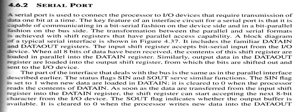
8 another program. When the transfer is completed, the DMA controller informs the processor by sending an interrupt request. In response, the OS puts the suspended program in the Runnable state so that it can be selected by the scheduler to continue execution An example of a computer system is given in above figure, showing how DMA controllers may be used. A DMA controller connects a high-speed network to the computer bus. The disk controller, which controls two disks, also has DMA capability and provides two DMA channels. It can perform two independent DMA operations, as if each disk had its own DMA controller. The registers needed to store the memory address, the word count, and so on are duplicated, so that one set can be used with each device. To start a DMA transfer of a block of data from the main memory to one of the disks, a program writes the address and word count information into the registers of the corresponding channel of the disk controller. It also provides the disk controller with information to identify the data for future retrieval. The DMA controller proceeds independently to implement the specified operation. When the DMA transfer is completed. This fact is recorded in the status and control register of the DMA channel by setting the Done bit. At the same time, if the IE bit is set, the controller sends an interrupt request to the processor and sets the IRQ bit. The status register can also be used to record other information, such as whether the transfer took place correctly or errors occurred. Memory accesses by the processor and the DMA controller are interwoven. Requests by DMA devices for using the bus are always given higher priority than processor requests. Among different DMA devices, top priority is given to high-speed peripherals such as a disk, a high-speed network interface, or a graphics display device. Since the processor originates most memory access cycles, the DMA controller can be said to steal memory cycles from the processor. Hence, the interweaving technique is usually called cycle stealing. Alternatively, the DMA controller may be given exclusive access to the main memory to transfer a block of data without interruption. This is known as block or burst mode Most DMA controllers incorporate a data storage buffer. In the case of the network interface in figure 5 for example, the DMA controller reads a block of data from the main memory and stores it into its input buffer. This transfer takes place using burst mode at a speed appropriate to the memory and the computer bus. Then, the data in the buffer are transmitted over the network at the speed of the network Q.5 a. Explain SERIAL PORT and draw a block diagram of a typical SERIAL INTERFACE. (8) IETE 8
9 IETE 9
 UNIVERSAL SERIAL BUS (USB):-The synergy between computers and communication is at the heart of today s information technology revolution.")
10 b. Explain the universal serial bus (USB) in a computer system. (8) UNIVERSAL SERIAL BUS (USB):-The synergy between computers and communication is at the heart of today s information technology revolution. A modern computer system is likely to involve a wide variety of devices such as keyboards, microphones, cameras, speakers, and display devices. Most computers also have a wired or wireless connection to the Internet. A key requirement is such an environment is the availability of a simple, low-cost mechanism to connect these devices to the computer, and an important recent development in this regard is the introduction of the Universal Serial Bus (USB). This is an industry standard developed through a collaborative effort of several computer and communication companies, including Compaq, Hewlett-Packard, Intel, Lucent, Microsoft, Nortel Networks, and Philips. The USB supports two speeds of operation, called low-speed (1.5 megabits/s) and full-speed (12 megabits/s). The most recent revision of the bus specification (USB 2.0) introduced a third speed of operation, called high-speed (480 megabits/s). The USB is quickly gaining acceptance in the market place, and with the addition of the high-speed capability it may well become the interconnection method of choice for most computer devices. The USB has been designed to meet several key objectives Provides a simple, low-cost and easy to use interconnection system that overcomes the difficulties due to the limited number of I/O ports available on a computer. Accommodate a wide range of data transfer characteristics for I/O devices, including telephone and Internet connections. Enhance user convenience through a plug-and-play mode of operation Port Limitation:-The parallel and serial ports described in previous section provide a generalpurpose point of connection through which a variety of low-to medium-speed devices can be connected to a computer. For practical reasons, only a few such ports are provided in a typical computer. Device Characteristics:-The kinds of devices that may be connected to a computer cover a wide range of functionality. The speed, volume, and timing constraints associated with data transfers to and from such devices vary significantly. A variety of simple devices that may be attached to a computer generate data of a similar nature low speed and asynchronous. Computer mice and the controls and manipulators used with video games are good examples. Plug-and-Play:-As computers become part of everyday life, their existence should become increasingly transparent. For example, when operating a home theater system, which includes at least one computer, IETE 10
11 the user should not find it necessary to turn the computer off or to restart the system to connect or disconnect a device. The plug-and-play feature means that a new device, such as an additional speaker, can be connected at any time while the system is operating. The system should detect the existence of this new device automatically, identify the appropriate device-driver software and any other facilities needed to service that device, and establish the appropriate addresses and logical connections to enable them to communicate. The plug-and-play requirement has many implications at all levels in the system, from the hardware to the operating system and the applications software. One of the primary objectives of the design of the USB has been to provide a plug-and-play capability USB Architecture:-The discussion above points to the need for an interconnection system that combines low cost, flexibility, and high data-transfer bandwidth. Also, I/O devices may be located at some distance from the computer to which they are connected. The requirement for high bandwidth would normally suggest a wide bus that carries 8, 16, or more bits in parallel. However, a large number of wires increases cost and complexity and is inconvenient to the user. Also, it is difficult to design a wide bus that carries data for a long distance because of the data skew problem discussed. The amount of skew increases with distance and limits the data that can be used A serial transmission format has been chosen for the USB because a serial bus satisfies the low-cost and flexibility requirements. Clock and data information are encoded together and transmitted as a single signal. Hence, there are no limitations on clock frequency or distance arising from data skew. Therefore, it is possible to provide a high data transfer bandwidth by using a high clock frequency. As pointed out earlier, the USB offers three bit rates, ranging from 1.5 to 480 megabits/s, to suit the needs of different I/O devices. Q.6 a. Explain static memories and dynamic memories. (8) Static Memories-Bipolar as well as MOS memory cells using a flip-flop like structure to store information can maintain the information as long as current flow to the cell is maintained. Such memories are called static memories. In contracts, Dynamic memories require not only the maintaining of a power supply, but also a periodic refresh to maintain the information stored in them. Dynamic memories can have very high bit densities and very lower power consumption relative to static memories and are thus generally used to realize the main memory unit. Dynamic Memories:-The basic idea of dynamic memory is that information is stored in the form of a charge on the capacitor. An example of a dynamic memory cell is shown below, when the transistor T is turned on and an appropriate voltage is applied to the bit line, information is stored in the cell, in the form of a known amount of charge stored on the capacitor. After the transistor is turned off, the capacitor begins to discharge. This is caused by the capacitor s own leakage resistance and the very small amount of current that still flows through the transistor. Hence the data is read correctly only if is read before the charge on the capacitor drops below some threshold value. During a Read operation, operation, the bit line is placed in a high-impendance state, the transistor is turned on and a sense circuit connected to the bit line is used to determine whether the charge on the capacitor is above or below the threshold value. During such a Read, the charge on the capacitor is restored to its original value and thus the cell is refreshed with every read operation. The cells are organized in the form of a square array such that the high-and lower-order 8 bits of the 16- bit address constitute the row and column addresses of a cell, respectively. In order to reduce the number of pins needed for external connections, the row and column address are multiplexed on 8 pins. To access a cell, the row address is applied first. It is loaded into the row address latch in response to a single pulse on the Row Address Strobe (RAS) input. This selects a row of cells. Now, the column address is applied to the address pins and is loaded into the column address latch under the control of the Column Address Strobe (CAS) input and this address selects the appropriate sense/write circuit. If the R/W signal indicates a Read operation, the output of the selected circuit is transferred to the data output. Do. For a write operation, the data on the DI line is used to overwrite the cell selected IETE 11
12 It is important to note that the application of a row address causes all the cells on the corresponding row to be read and refreshed during both Read and Write operations. To ensure that the contents of a dynamic memory are maintained, each row of cells must be addressed periodically, typically once every two milliseconds. A Refresh circuit performs this function. Some dynamic memory chips incorportate a refresh facility the chips themselves and hence they appear as static memories to the user! such chips are often referred to as Pseudostatic. Another feature available on many dynamic memory chips is that once the row address is loaded, successive locations can be accessed by loading only column addresses. Such block transfers can be carried out typically at a rate that is double that for transfers involving random addresses. Such a feature is useful when memory access follow a regular pattern, for example, in a graphics terminal. Because of their high density and low cost, dynamic memories are widely used in the main memory units of computers. Commercially available chips range in size from 1k to 4M bits or more, and are available in various organizations like 64k x 1, 16k x 4, 1MB x 1 etc. b. What is cache memory? Explain associative mapping cache. (8) CACHE MEMORY:Analysis of a large number of typical programs has shown that most of their execution time is spent on a few main row lines in which a number of instructions are executed repeatedly. These instructions may constitute a simple loop, nested loops or few procedures that repeatedly call each other. The main observation is that many instructions in a few localized are as of the program are repeatedly executed and that the remainder of the program is accessed relatively infrequently. This phenomenan is referred to as locality of reference. If the active segments of a program can be placed in a fast memory, then the total execution time can be significantly reduced, such a memory is referred as a cache memory which is in served between the CPU and the main memory as shown in fig.1 cache memory between main memory & CPU CPU CACHE Main memory Two Level memory Hierarchy: We will adopt the terms Primary level for the smaller, faster memory and the secondary level for larger, slower memory, we will also allow cache to be a primary level with slower semiconductor memory as the corresponding secondary level. At a different point in the hierarchy, the same S.C memory could be the primary level with disk as the secondary level. Primary and Secondary addresses:-a two level hierarchy and its addressing are illustrated in fig.2. A system address is applied to the memory management unit (MMU) that handles the mapping function for the particular pair in the hierarchy. If the MMU finds the address in the Primary level, it provides Primary address, which selects the item from the Primary memory. This translation must be fast, because every time memory is accessed, the system address must be translated. The translation may fail to produce a Primary address because the requested items is not found, so that information can be retrieved from the secondary level and transferred to the Primary level IETE 12
13 Hits and Misses:- Successful translation of reference into Primary address is called a hit, and failure is a miss. The hit ratio is (1-miss ratio). If tp is the Primary memory access time and ts is the secondary access time, the average access time for the two level hierarchy is ta = h tp + (1-h)ts Associative mapped caches:-main memory can be placed anywhere in the cache. After being placed in the cache, a given block is identified uniquely by its main memory block number, referred to as the tag, which is stored inside a separate tag memory in the cache. Regardless of the kind of cache, a given block in the cache may or may not contain valid information. For example, when the system has just been powered up add before the cache has had any blocks loaded into it, all the information there is invalid. The cache maintains a valid bit for each block to keep track of whether the information in the corresponding block is valid. In figure shows the various memory structures in an associative cache, The cache itself contain 256, 8byte blocks, a 256 x 13 bit tag memory for holding the tags of the blocks currently stored in the cache, and a 256 x 1 bit memory for storing the valid bits, Main memory contains 8192, 8 byte blocks. The figure indicates that main memory address references are partition into two fields, a 3 bit word field describing the location of the desired word in the cache line, and a 13 bit tag field describing the main memory block number desired. The 3 bit word field becomes essentially a cache address specifying where to find the word if indeed it is in the cache. The remaining 13 bits must be compared against every 13 bit tag in the tag memory to see if the desired word is present. In the fig, above, main memory block 2 has been stored in the 256 cache block and so the 256th tag entry is 2 mm block 119 has been stored in the second cache block corresponding entry in tag memory is 119 mm block 421 has been stored in cache block 0 and tag memory location 0 has been set to 421. Three valid bits have also been set, indicating valid information in these locations. The associative cache makes the most flexible and complete use of its capacity, storing blocks wherever it needs to, but there is a penalty to be paid for this flexibility the tag memory must be searched in for each memory reference IETE 13
14 Q.7 a. What is virtual memory? Write down the advantages of virtual memory. (8) Virtual Memory:-Virtual memory is the technique of using secondary storage such as disks to enter the apparent size of accessible memory beyond its actual physical size. Virtual memory is implemented by employing a memory-management unit (MMU) to translate every logical address reference into a physical address reference as shown in fig 1. The MMU is imposed between the CPU and the physical memory where it performs these translations under the control of the operating system. Each memory reference is sued by the CPU is translated from the logical address space to the physical address space. Mapping tables guide the translation, again under the control of the operating system. Virtual memory usually demand paging, which means that a Page is moved from disk into main memory only when the processor accesses a word on that page. Virtual memory pages always have a place on the disk once they are created, but are copied to main memory only on a miss or page fault. Advantages of Virtual memory:- 1. Simplified addressing:- Each program unit can be compiled into its own memory space, beginning at address O and extending far beyond the limits of physical memory. Programs and data structures do not require address relocation at load time, nor must they be broken into fragments merely to accommodate memory limitations 2. Cost effective use of memory: - Less expensive disk storage can replace more expensive RAM memory, since the entire program does not need to occupy physical memory at one time. 3. Access control: - Since each memory reference must be translated, it can be simultaneously checked for read, write and execute privileges. This allows hardward level control of access to system resources IETE 14
 4 bit adder with carry look ahead logic-now, consider the design of a 4-bit parallel adder.")
15 and also prevents and also prevents buggy programs or intruders from causing damage to the resources of other users or the system b. Explain 4-bit adder with carry look ahead logic. (8) 4 bit adder with carry look ahead logic-now, consider the design of a 4-bit parallel adder. The carries can be implemented as The complete 4-bit adder is shown in Figure 5b where the B cell indicates Gi, Pi & Si generator. The carries are implemented in the block labeled carry look-ahead logic. An adder implemented in this form is called a carry look ahead adder. Delay through the adder is 3 gate delays for all carry bits and 4 gate delays for all sum bits. In comparison, note that a 4-bit ripple-carry adder requires 7 gate delays for S3(2n-1) and 8 gate delays(2n) for c4. IETE 15
 Booth algo flow chart-the Booth algorithm generates a 2n-bit product and both positive and negative 2's-complement n-bit operands are uniformly treated.")
16 Q.8 a. Explain booth multiplication algorithm. (8) Booth algo flow chart-the Booth algorithm generates a 2n-bit product and both positive and negative 2's-complement n-bit operands are uniformly treated. To understand this algorithm, consider a multiplication operation in which the multiplier is positive and has a single block of 1s, for example, (+30). To derive the product, as in the normal standard procedure, we could add four appropriately shifted versions of the multiplicand. However, using the Booth algorithm, we can reduce the number of required operations by regarding this multiplier as the difference between numbers 32 & 2 as shown below This suggests that the product can be generated by adding 25 times the multiplicand to the 2's-complement of 21 times the multiplicand. For convenience, we can describe the sequence of required operations by recoding the preceding multiplier as In general, in the Booth scheme, -1 times the shifted multiplicand is selected when moving from 0 to 1, and +1 times the shifted multiplicand is selected when moving from 1 to 0, as the multiplier is scanned from right to left IETE 16

17 b. Explain the circuit diagram for restoring division. (8) Restoring Division: Figure shows a logic circuit arrangement that implements restoring division. Note its similarity to the structure for multiplication that was shown in Figure 8. An n-bit positive divisor is loaded into register M and an n-bit positive dividend is loaded into register Q at the start of the operation. Register A is set to 0. After the division is complete, the n-bit quotient is in register Q and the remainder is in register A. The required subtractions are facilitated by using 2's-complement arithmetic. The extra bit position at the left end of both A and M accommodates the sign bit during subtractions. The following algorithm performs restoring division. Do the following n times: 1. Shift A and Q left one binary position. 2. Subtract M from A, and place the answer back in A. 3. If the sign of A is 1, set q0 to 0 and add M back to A (that is, restore A); otherwise, set q0to 1 Q.9 a. Explain execution of a complete instruction. (8) EXECUTION OF A COMPLETE INSTRUCTION:Let us now put together the sequence of elementary operations required to execute one instruction. Consider the instruction Add (R3), R1 which adds the contents of a memory location pointed to by R3 to register R1. Executing this instruction requires the following actions: 1. Fetch the instruction. 2. Fetch the first operand (the contents of the memory location pointed to by R3). IETE 17
18 3. Perform the addition. 4.Load the result into Rl. In figure above indicates the sequence of control steps required to perform these operations for the single-bus architecture of Figure 2. Instruction execution proceeds as follows. In step 1, the instruction fetch operation is initiated by loading the contents of the PC into the MAR and sending a Read request to the memory. The Select signal is set to Select4, which causes the multiplexer MUX to select the constant 4. This value is added to the operand at input B, which is the contents of the PC, and the result is stored in register Z. The updated value is moved from register Z back into the PC during step 2, while waiting for the memory to respond. In step 3, the word fetched from the memory is loaded into the IR. Steps 1 through 3 constitute the instruction fetch phase, which is the same for all instructions. The instruction decoding circuit interprets the contents of the IR at the beginning of step 4. This enables the control circuitry to activate the control signals for steps 4 through 7, which constitute the execution phase. The contents of register R3 are transferred to the MAR in step 4, and a memory read operation is initiated. Then the contents of Rl are transferred to register Y in step 5, to prepare for the addition operation. When the Read operation is completed, the memory operand is available in register MDR, and the addition operation is performed in step 6. The contents of MDR are gated to the bus, and thus also to the B input of the ALU, and register Y is selected as the second input to the ALU by choosing Select Y. The sum is stored in register Z, then transferred to Rl in step 7. The End signal causes a new instruction fetch cycle to begin by returning to step 1. Branch Instructions: A branch instruction replaces the contents of the PC with the branch target address. This address is usually obtained by adding an offset X, which is given in the branch instruction, to the updated value of the PC. Listing in figure 8 below gives a control sequence that implements an unconditional branch instruction. Processing starts, as usual, with the fetch phase. This phase ends when the instruction is loaded into the IR in step 3. The offset value is extracted from the IR by the instruction decoding circuit, which will also perform sign extension if required. Since the value of the updated PC is already available in register Y, the offset X is gated onto the bus in step 4, and an addition operation is performed. The result, which is the branch target address, is loaded A branch instruction replaces the contents of the PC with the branch target address. This address is usually obtained by adding an offset X, which is given in the branch instruction, to the updated value of the PC. Listing in figure 8 below gives a control sequence that implements an unconditional branch instruction. Processing starts, as usual, with the fetch phase. This phase ends when the instruction is loaded into the IR in step 3. The offset value is extracted from the IR by the instruction decoding circuit, which will also perform sign extension if required. Since the value of the updated PC is already available in register Y, the offset X is gated onto the bus in step 4, and an addition operation is performed. The result, which is the branch target address, is loaded into the PC in step 5.The offset X used in a branch instruction is usually the difference between the branch target address and the address immediately following the branch instruction IETE 18
19 b. Explain microprogrammed control in detail. (8) MICROPROGRAMMED CONTROL: ALU is the heart of any computing system, while Control unit is its brain. The design of a control unit is not unique; it varies from designer to designer. Some of the commonly used control logic design methods are; Sequence Reg & Decoder method Hard-wired control method PLA control method Micro-program control method The control signals required inside the processor can be generated using a control step counter and a decoder/ encoder circuit. Now we discuss an alternative scheme, called micro programmed control, in which control signals are generated by a program similar to machine language programs A control word (CW) is a word whose individual bits represent the various control signals in Figure 12. Each of the control steps in the control sequence of an instruction defines a unique combination of Is and Os in the CW. The CWs corresponding to the 7 steps. We have assumed that Select Y is epresented by Select = 0 and Select4 by Select = 1. A sequence of CWs corresponding to the control sequence of a machine instruction constitutes the micro routine for that instruction, and the individual control words in this micro routine are referred to as microinstructions The micro routines for all instructions in the instruction set of a computer are stored in a special memory called the control store. The control unit can generate the control signals for any instruction by sequentially reading the CWs of the corresponding micro routine from the control store. This suggests organizing the control unit as shown in Figure 16. To read the control words sequentially from the control store, a micro program counter (μpc) is used. Every time a new instruction is loaded into the IR, the output of the block labeled "starting address generator" is loaded into the μpc. The μpc is then automatically incremented by the clock, causing successive microinstructions to be read from the control store. Hence, the control signals are delivered to various parts of the processor in the correct sequence IETE 19
Basic Processing Unit: Some Fundamental Concepts, Execution of a. Complete Instruction, Multiple Bus Organization, Hard-wired Control,
 UNIT - 7 Basic Processing Unit: Some Fundamental Concepts, Execution of a Complete Instruction, Multiple Bus Organization, Hard-wired Control, Microprogrammed Control Page 178 UNIT - 7 BASIC PROCESSING
Computer Architecture
 Computer Architecture Lecture 1: Digital logic circuits The digital computer is a digital system that performs various computational tasks. Digital computers use the binary number system, which has two
ADVANCED COMPUTER ARCHITECTURE TWO MARKS WITH ANSWERS
 ADVANCED COMPUTER ARCHITECTURE TWO MARKS WITH ANSWERS 1.Define Computer Architecture Computer Architecture Is Defined As The Functional Operation Of The Individual H/W Unit In A Computer System And The
PESIT Bangalore South Campus
 INTERNAL ASSESSMENT TEST I Date: 30/08/2017 Max Marks: 40 Subject & Code: Computer Organization 15CS34 Semester: III (A & B) Name of the faculty: Mrs.Sharmila Banu.A Time: 8.30 am 10.00 am Answer any FIVE
Module 5 - CPU Design
 Module 5 - CPU Design Lecture 1 - Introduction to CPU The operation or task that must perform by CPU is: Fetch Instruction: The CPU reads an instruction from memory. Interpret Instruction: The instruction
Chapter 3 Machine Instructions & Programs. Jin-Fu Li Department of Electrical Engineering National Central University Jungli, Taiwan
 Chapter 3 Machine Instructions & Programs Jin-Fu Li Department of Electrical Engineering National Central University Jungli, Taiwan Outline Numbers, Arithmetic Operations, and Characters Memory Locations
Advanced Parallel Architecture Lesson 3. Annalisa Massini /2015
 Advanced Parallel Architecture Lesson 3 Annalisa Massini - 2014/2015 Von Neumann Architecture 2 Summary of the traditional computer architecture: Von Neumann architecture http://williamstallings.com/coa/coa7e.html
DC57 COMPUTER ORGANIZATION JUNE 2013
 Q2 (a) How do various factors like Hardware design, Instruction set, Compiler related to the performance of a computer? The most important measure of a computer is how quickly it can execute programs.
PESIT Bangalore South Campus
 INTERNAL ASSESSMENT TEST III Date : 21/11/2017 Max Marks : 40 Subject & Code : Computer Organization (15CS34) Semester : III (A & B) Name of the faculty: Mrs. Sharmila Banu Time : 11.30 am 1.00 pm Answer
COMPUTER ORGANISATION CHAPTER 1 BASIC STRUCTURE OF COMPUTERS
 Computer types: - COMPUTER ORGANISATION CHAPTER 1 BASIC STRUCTURE OF COMPUTERS A computer can be defined as a fast electronic calculating machine that accepts the (data) digitized input information process
2 MARKS Q&A 1 KNREDDY UNIT-I
 2 MARKS Q&A 1 KNREDDY UNIT-I 1. What is bus; list the different types of buses with its function. A group of lines that serves as a connecting path for several devices is called a bus; TYPES: ADDRESS BUS,
UNIT I BASIC STRUCTURE OF COMPUTERS Part A( 2Marks) 1. What is meant by the stored program concept? 2. What are the basic functional units of a
 1. What is meant by the stored program concept? 2. What are the basic functional units of a") UNIT I BASIC STRUCTURE OF COMPUTERS Part A( 2Marks) 1. What is meant by the stored program concept? 2. What are the basic functional units of a computer? 3. What is the use of buffer register? 4. Define
UNIT I BASIC STRUCTURE OF COMPUTERS Part A( 2Marks) 1. What is meant by the stored program concept? 2. What are the basic functional units of a computer? 3. What is the use of buffer register? 4. Define
COMPUTER ARCHITECTURE AND ORGANIZATION Register Transfer and Micro-operations 1. Introduction A digital system is an interconnection of digital
 Register Transfer and Micro-operations 1. Introduction A digital system is an interconnection of digital hardware modules that accomplish a specific information-processing task. Digital systems vary in
COA. Prepared By: Dhaval R. Patel Page 1. Q.1 Define MBR.
 Q.1 Define MBR. MBR( Memory buffer register) A Memory Buffer Register (MBR) is the register in a computers processor that stores the data being transferred to and from the devices It allowing the processor
MaanavaN.Com CS1202 COMPUTER ARCHITECHTURE
 DEPARTMENT OF COMPUTER SCIENCE AND ENGINEERING QUESTION BANK SUB CODE / SUBJECT: CS1202/COMPUTER ARCHITECHTURE YEAR / SEM: II / III UNIT I BASIC STRUCTURE OF COMPUTER 1. What is meant by the stored program
Vtusolution.in COMPUTER ORGANIZATION. Subject Code: 10CS46 PART A
 COMPUTER ORGANIZATION Subject Code: UNIT-1 PART A 6 Hours Basic Structure of Computers: Computer Types, Functional Units, Basic Operational Concepts, Bus Structures, Performance Processor Clock, Basic
Advanced Parallel Architecture Lesson 3. Annalisa Massini /2015
 Advanced Parallel Architecture Lesson 3 Annalisa Massini - Von Neumann Architecture 2 Two lessons Summary of the traditional computer architecture Von Neumann architecture http://williamstallings.com/coa/coa7e.html
ASSEMBLY LANGUAGE MACHINE ORGANIZATION
 ASSEMBLY LANGUAGE MACHINE ORGANIZATION CHAPTER 3 1 Sub-topics The topic will cover: Microprocessor architecture CPU processing methods Pipelining Superscalar RISC Multiprocessing Instruction Cycle Instruction
MARTHANDAM COLLEGE OF ENGINEERING AND TECHNOLOGY DEPARTMENT OF INFORMATION TECHNOLOGY TWO MARK QUESTIONS AND ANSWERS
 MARTHANDAM COLLEGE OF ENGINEERING AND TECHNOLOGY DEPARTMENT OF INFORMATION TECHNOLOGY TWO MARK QUESTIONS AND ANSWERS SUB NAME: COMPUTER ORGANIZATION AND ARCHITECTTURE SUB CODE: CS 2253 YEAR/SEM:II/IV Marthandam
COMPUTER ORGANIZATION AND ARCHITECTURE
 Page 1 1. Which register store the address of next instruction to be executed? A) PC B) AC C) SP D) NONE 2. How many bits are required to address the 128 words of memory? A) 7 B) 8 C) 9 D) NONE 3. is the
SUBROUTINE NESTING AND THE PROCESSOR STACK:-
 SUBROUTINE NESTING AND THE PROCESSOR STACK:- A common programming practice, called subroutine nesting, is to have one subroutine call another. In this case, the return address of the second call is also
2. ADDRESSING METHODS
 2 Addressing Methods STUDY MATERIALS ON COMPUTER ORGANIZATION (As per the curriculum of Third semester BSc Electronics of Mahatma Gandh Uniiversity) Compiled by Sam Kollannore U Lecturer in Electronics
Unit 3 and Unit 4: Chapter 4 INPUT/OUTPUT ORGANIZATION
 Unit 3 and Unit 4: Chapter 4 INPUT/OUTPUT ORGANIZATION Introduction A general purpose computer should have the ability to exchange information with a wide range of devices in varying environments. Computers
UNIT-II. Part-2: CENTRAL PROCESSING UNIT
 Page1 UNIT-II Part-2: CENTRAL PROCESSING UNIT Stack Organization Instruction Formats Addressing Modes Data Transfer And Manipulation Program Control Reduced Instruction Set Computer (RISC) Introduction:
Digital System Design Using Verilog. - Processing Unit Design
 Digital System Design Using Verilog - Processing Unit Design 1.1 CPU BASICS A typical CPU has three major components: (1) Register set, (2) Arithmetic logic unit (ALU), and (3) Control unit (CU) The register
UNIT 2 MACHINE INSTRUCTIONS & PROGRAMS (CONT.)
") 1 UNIT 2 MACHINE INSTRUCTIONS & PROGRAMS (CONT.) ADDRESSING MODES The different ways in which the location of an operand is specified in an instruction are referred to as addressing modes (Table 2.1).
1 UNIT 2 MACHINE INSTRUCTIONS & PROGRAMS (CONT.) ADDRESSING MODES The different ways in which the location of an operand is specified in an instruction are referred to as addressing modes (Table 2.1).
STRUCTURE OF DESKTOP COMPUTERS
 Page no: 1 UNIT 1 STRUCTURE OF DESKTOP COMPUTERS The desktop computers are the computers which are usually found on a home or office desk. They consist of processing unit, storage unit, visual display
COMPUTER ORGANIZATION AND ARCHITECTURE
 COMPUTER ORGANIZATION AND ARCHITECTURE For COMPUTER SCIENCE COMPUTER ORGANIZATION. SYLLABUS AND ARCHITECTURE Machine instructions and addressing modes, ALU and data-path, CPU control design, Memory interface,
4 MEMORY SYSTEM 4.1 BASIC CONCEPTS:
 4 MEMORY SYSTEM 4.1 BASIC CONCEPTS: The maximum size of the Main Memory (MM) that can be used in any computer is determined by its addressing scheme. For example, a 16-bit computer that generates 16-bit
UNIT I DATA REPRESENTATION, MICRO-OPERATIONS, ORGANIZATION AND DESIGN
 UNIT I DATA REPRESENTATION, MICRO-OPERATIONS, ORGANIZATION AND DESIGN Data representation: Data types, complements, fixed point representation, floating-point representation, other binary codes, error
PART A (22 Marks) 2. a) Briefly write about r's complement and (r-1)'s complement. [8] b) Explain any two ways of adding decimal numbers.
![PART A (22 Marks) 2. a) Briefly write about r's complement and (r-1)'s complement. [8] b) Explain any two ways of adding decimal numbers.](/thumbs/96/128058841.jpg "PART A (22 Marks) 2. a) Briefly write about r's complement and (r-1)'s complement. [8] b) Explain any two ways of adding decimal numbers.") Set No. 1 IV B.Tech I Semester Supplementary Examinations, March - 2017 COMPUTER ARCHITECTURE & ORGANIZATION (Common to Electronics & Communication Engineering and Electronics & Time: 3 hours Max. Marks:
Set No. 1 IV B.Tech I Semester Supplementary Examinations, March - 2017 COMPUTER ARCHITECTURE & ORGANIZATION (Common to Electronics & Communication Engineering and Electronics & Time: 3 hours Max. Marks:
k -bit address bus n-bit data bus Control lines ( R W, MFC, etc.)
") THE MEMORY SYSTEM SOME BASIC CONCEPTS Maximum size of the Main Memory byte-addressable CPU-Main Memory Connection, Processor MAR MDR k -bit address bus n-bit data bus Memory Up to 2 k addressable locations
THE MEMORY SYSTEM SOME BASIC CONCEPTS Maximum size of the Main Memory byte-addressable CPU-Main Memory Connection, Processor MAR MDR k -bit address bus n-bit data bus Memory Up to 2 k addressable locations
Concept of Memory. The memory of computer is broadly categories into two categories:
 Concept of Memory We have already mentioned that digital computer works on stored programmed concept introduced by Von Neumann. We use memory to store the information, which includes both program and data.
Register Transfer and Micro-operations
 Register Transfer Language Register Transfer Bus Memory Transfer Micro-operations Some Application of Logic Micro Operations Register Transfer and Micro-operations Learning Objectives After reading this
b) Write basic performance equation.
 Write basic performance equation.") 1. a) What is use of buffers? Ans: The Buffer Register prevents the high speed processor from being locked to a slow I/O device during a sequence of data transfer or reduces speed mismatch between faster
1. a) What is use of buffers? Ans: The Buffer Register prevents the high speed processor from being locked to a slow I/O device during a sequence of data transfer or reduces speed mismatch between faster
 Part A Questions 1. What is an ISP? ISP stands for Instruction Set Processor. This unit is simply called as processor which executes machine instruction and coordinates the activities of other units..
Introduction to CPU Design
 ١ Introduction to CPU Design Computer Organization & Assembly Language Programming Dr Adnan Gutub aagutub at uqu.edu.sa [Adapted from slides of Dr. Kip Irvine: Assembly Language for Intel-Based Computers]
14 CS / IT 403 II/IV B.Tech (Regular)DEGREE EXAMINATION
DEGREE EXAMINATION") 14 CS / IT 403 II/IV B.Tech (Regular)DEGREE EXAMINATION JUNE,2016 Fourth Semester Time:Three Hours Answer Question No 1 Compulsorily. Answer ONE Question from each unit. Computer Organization Maximum:
14 CS / IT 403 II/IV B.Tech (Regular)DEGREE EXAMINATION JUNE,2016 Fourth Semester Time:Three Hours Answer Question No 1 Compulsorily. Answer ONE Question from each unit. Computer Organization Maximum:
AC58/AT58 COMPUTER ORGANIZATION DECEMBER Q2 (a) With the help of diagram explain the different functional units of a Computer?
 With the help of diagram explain the different functional units of a Computer?") Q2 (a) With the help of diagram explain the different functional units of a Computer? Answer: A computer consists of five functionally independent units, namely: input, memory, arithmetic and logic (ALU)
Q2 (a) With the help of diagram explain the different functional units of a Computer? Answer: A computer consists of five functionally independent units, namely: input, memory, arithmetic and logic (ALU)
SAE5C Computer Organization and Architecture. Unit : I - V
 SAE5C Computer Organization and Architecture Unit : I - V UNIT-I Evolution of Pentium and Power PC Evolution of Computer Components functions Interconnection Bus Basics of PCI Memory:Characteristics,Hierarchy
PROBLEMS. 7.1 Why is the Wait-for-Memory-Function-Completed step needed when reading from or writing to the main memory?
 446 CHAPTER 7 BASIC PROCESSING UNIT (Corrisponde al cap. 10 - Struttura del processore) PROBLEMS 7.1 Why is the Wait-for-Memory-Function-Completed step needed when reading from or writing to the main memory?
Chapter 3 : Control Unit
 3.1 Control Memory Chapter 3 Control Unit The function of the control unit in a digital computer is to initiate sequences of microoperations. When the control signals are generated by hardware using conventional
UNIT - I: COMPUTER ARITHMETIC, REGISTER TRANSFER LANGUAGE & MICROOPERATIONS
 UNIT - I: COMPUTER ARITHMETIC, REGISTER TRANSFER LANGUAGE & MICROOPERATIONS (09 periods) Computer Arithmetic: Data Representation, Fixed Point Representation, Floating Point Representation, Addition and
Lecture 04: Machine Instructions
 CSCI2510 Computer Organization Lecture 04: Machine Instructions Ming-Chang YANG mcyang@cse.cuhk.edu.hk Reading: Chap. 2.3~2.4, 2.10~2.11 Recall: Instructions & Program A computer is governed by instructions.
Chapter 3 - Top Level View of Computer Function
 Chapter 3 - Top Level View of Computer Function Luis Tarrataca luis.tarrataca@gmail.com CEFET-RJ L. Tarrataca Chapter 3 - Top Level View 1 / 127 Table of Contents I 1 Introduction 2 Computer Components
UNIT - V MEMORY P.VIDYA SAGAR ( ASSOCIATE PROFESSOR) Department of Electronics and Communication Engineering, VBIT
 Department of Electronics and Communication Engineering, VBIT") UNIT - V MEMORY P.VIDYA SAGAR ( ASSOCIATE PROFESSOR) contents Memory: Introduction, Random-Access memory, Memory decoding, ROM, Programmable Logic Array, Programmable Array Logic, Sequential programmable
UNIT - V MEMORY P.VIDYA SAGAR ( ASSOCIATE PROFESSOR) contents Memory: Introduction, Random-Access memory, Memory decoding, ROM, Programmable Logic Array, Programmable Array Logic, Sequential programmable
CREATED BY M BILAL & Arslan Ahmad Shaad Visit:
 CREATED BY M BILAL & Arslan Ahmad Shaad Visit: www.techo786.wordpress.com Q1: Define microprocessor? Short Questions Chapter No 01 Fundamental Concepts Microprocessor is a program-controlled and semiconductor
Chapter 5 Input/Output Organization. Jin-Fu Li Department of Electrical Engineering National Central University Jungli, Taiwan
 Chapter 5 Input/Output Organization Jin-Fu Li Department of Electrical Engineering National Central University Jungli, Taiwan Outline Accessing I/O Devices Interrupts Direct Memory Access Buses Interface
Chapter 17. Microprogrammed Control. Yonsei University
 Chapter 17 Microprogrammed Control Contents Basic Concepts Microinstruction Sequencing Microinstruction Execution TI 8800 Applications of Microprogramming 17-2 Introduction Basic Concepts An alternative
JNTUWORLD. 1. Discuss in detail inter processor arbitration logics and procedures with necessary diagrams? [15]
![JNTUWORLD. 1. Discuss in detail inter processor arbitration logics and procedures with necessary diagrams? [15]](/thumbs/96/128058746.jpg "JNTUWORLD. 1. Discuss in detail inter processor arbitration logics and procedures with necessary diagrams? [15]") Code No: 09A50402 R09 Set No. 2 1. Discuss in detail inter processor arbitration logics and procedures with necessary diagrams? [15] 2. (a) Discuss asynchronous serial transfer concept? (b) Explain in
Code No: 09A50402 R09 Set No. 2 1. Discuss in detail inter processor arbitration logics and procedures with necessary diagrams? [15] 2. (a) Discuss asynchronous serial transfer concept? (b) Explain in
Unit objective. Unit Introduction UNIT - I. In this unit you will be introduced to :
 Unit objective In this unit you will be introduced to : UNIT - I The basic structure of a computer, Machine instructions and their execution, System software that enables the preparation and execution
Chapter 3. Top Level View of Computer Function and Interconnection. Yonsei University
 Chapter 3 Top Level View of Computer Function and Interconnection Contents Computer Components Computer Function Interconnection Structures Bus Interconnection PCI 3-2 Program Concept Computer components
CHETTINAD COLLEGE OF ENGINEERING AND TECHNOLOGY COMPUTER ARCHITECURE- III YEAR EEE-6 TH SEMESTER 16 MARKS QUESTION BANK UNIT-1
 CHETTINAD COLLEGE OF ENGINEERING AND TECHNOLOGY COMPUTER ARCHITECURE- III YEAR EEE-6 TH SEMESTER 16 MARKS QUESTION BANK UNIT-1 Data representation: (CHAPTER-3) 1. Discuss in brief about Data types, (8marks)
The von Neumann Architecture. IT 3123 Hardware and Software Concepts. The Instruction Cycle. Registers. LMC Executes a Store.
 IT 3123 Hardware and Software Concepts February 11 and Memory II Copyright 2005 by Bob Brown The von Neumann Architecture 00 01 02 03 PC IR Control Unit Command Memory ALU 96 97 98 99 Notice: This session
EE 3170 Microcontroller Applications
 EE 3170 Microcontroller Applications Lecture 4 : Processors, Computers, and Controllers - 1.2 (reading assignment), 1.3-1.5 Based on slides for ECE3170 by Profs. Kieckhafer, Davis, Tan, and Cischke Outline
PESIT Bangalore South Campus
 Fourth Semester B.E. IA Test-1, 2015 USN 1 P E I S PESIT Bangalore South Campus (Hosur Road, 1KM before Electronic City, Bangalore-560 100) Department of Information Science & Engineering Section: 4 th
Q.1 Explain Computer s Basic Elements
 Q.1 Explain Computer s Basic Elements Ans. At a top level, a computer consists of processor, memory, and I/O components, with one or more modules of each type. These components are interconnected in some
INPUT-OUTPUT ORGANIZATION
 INPUT-OUTPUT ORGANIZATION Peripheral Devices: The Input / output organization of computer depends upon the size of computer and the peripherals connected to it. The I/O Subsystem of the computer, provides
Latches. IT 3123 Hardware and Software Concepts. Registers. The Little Man has Registers. Data Registers. Program Counter
 IT 3123 Hardware and Software Concepts Notice: This session is being recorded. CPU and Memory June 11 Copyright 2005 by Bob Brown Latches Can store one bit of data Can be ganged together to store more
Class Notes. Dr.C.N.Zhang. Department of Computer Science. University of Regina. Regina, SK, Canada, S4S 0A2
 Class Notes CS400 Part VI Dr.C.N.Zhang Department of Computer Science University of Regina Regina, SK, Canada, S4S 0A2 C. N. Zhang, CS400 83 VI. CENTRAL PROCESSING UNIT 1 Set 1.1 Addressing Modes and Formats
AC58/AT58/AC106/AT106 COMPUTER ORGANIZATION DEC 2015
 Q.2 a. With the help of diagram, explain the different functional units of a Computer. (6) A computer consists of five functionally independent main parts: input, memory, arithmetic and logic, output,
chapter 8 The Memory System Chapter Objectives
 chapter 8 The Memory System Chapter Objectives In this chapter you will learn about: Basic memory circuits Organization of the main memory Memory technology Direct memory access as an I/O mechanism Cache
Computer Organization and Assembly Language
 Computer Organization and Assembly Language Week 01 Nouman M Durrani COMPUTER ORGANISATION AND ARCHITECTURE Computer Organization describes the function and design of the various units of digital computers
Chapter 4. MARIE: An Introduction to a Simple Computer
 Chapter 4 MARIE: An Introduction to a Simple Computer Chapter 4 Objectives Learn the components common to every modern computer system. Be able to explain how each component contributes to program execution.
Computer Systems Organization
 The IAS (von Neumann) Machine Computer Systems Organization Input Output Equipment Stored Program concept Main memory storing programs and data ALU operating on binary data Control unit interpreting instructions
Chapter 4. MARIE: An Introduction to a Simple Computer. Chapter 4 Objectives. 4.1 Introduction. 4.2 CPU Basics
 Chapter 4 Objectives Learn the components common to every modern computer system. Chapter 4 MARIE: An Introduction to a Simple Computer Be able to explain how each component contributes to program execution.
Question Bank Microprocessor and Microcontroller
 QUESTION BANK - 2 PART A 1. What is cycle stealing? (K1-CO3) During any given bus cycle, one of the system components connected to the system bus is given control of the bus. This component is said to
CPE300: Digital System Architecture and Design
 CPE300: Digital System Architecture and Design Fall 2011 MW 17:30-18:45 CBC C316 Cache 11232011 http://www.egr.unlv.edu/~b1morris/cpe300/ 2 Outline Review Memory Components/Boards Two-Level Memory Hierarchy
Blog -
 . Instruction Codes Every different processor type has its own design (different registers, buses, microoperations, machine instructions, etc) Modern processor is a very complex device It contains Many
Processing Unit CS206T
 Processing Unit CS206T Microprocessors The density of elements on processor chips continued to rise More and more elements were placed on each chip so that fewer and fewer chips were needed to construct
GUJARAT TECHNOLOGICAL UNIVERSITY MASTER OF COMPUTER APPLICATION SEMESTER: III
 GUJARAT TECHNOLOGICAL UNIVERSITY MASTER OF COMPUTER APPLICATION SEMESTER: III Subject Name: Operating System (OS) Subject Code: 630004 Unit-1: Computer System Overview, Operating System Overview, Processes
INTELLIGENCE PLUS CHARACTER - THAT IS THE GOAL OF TRUE EDUCATION UNIT-I
 UNIT-I 1. List and explain the functional units of a computer with a neat diagram 2. Explain the computer levels of programming languages 3. a) Explain about instruction formats b) Evaluate the arithmetic
CPU ARCHITECTURE. QUESTION 1 Explain how the width of the data bus and system clock speed affect the performance of a computer system.
 CPU ARCHITECTURE QUESTION 1 Explain how the width of the data bus and system clock speed affect the performance of a computer system. ANSWER 1 Data Bus Width the width of the data bus determines the number
INPUT/OUTPUT ORGANIZATION
 INPUT/OUTPUT ORGANIZATION Accessing I/O Devices I/O interface Input/output mechanism Memory-mapped I/O Programmed I/O Interrupts Direct Memory Access Buses Synchronous Bus Asynchronous Bus I/O in CO and
Chapter 14 Design of the Central Processing Unit
 Chapter 14 Design of the Central Processing Unit We now focus on the detailed design of the CPU (Central Processing Unit) of the Boz 7. The CPU has two major components: the Control Unit and the ALU (Arithmetic
3.1 Description of Microprocessor. 3.2 History of Microprocessor
 3.0 MAIN CONTENT 3.1 Description of Microprocessor The brain or engine of the PC is the processor (sometimes called microprocessor), or central processing unit (CPU). The CPU performs the system s calculating
Blog - https://anilkumarprathipati.wordpress.com/
 Control Memory 1. Introduction The function of the control unit in a digital computer is to initiate sequences of microoperations. When the control signals are generated by hardware using conventional
Computer Organisation CS303
 Computer Organisation CS303 Module Period Assignments 1 Day 1 to Day 6 1. Write a program to evaluate the arithmetic statement: X=(A-B + C * (D * E-F))/G + H*K a. Using a general register computer with
INPUT/OUTPUT ORGANIZATION
 INPUT/OUTPUT ORGANIZATION Accessing I/O Devices I/O interface Input/output mechanism Memory-mapped I/O Programmed I/O Interrupts Direct Memory Access Buses Synchronous Bus Asynchronous Bus I/O in CO and
Basics of Microprocessor
 Unit 1 Basics of Microprocessor 1. Microprocessor Microprocessor is a multipurpose programmable integrated device that has computing and decision making capability. This semiconductor IC is manufactured
Lecture 11: Control Unit and Instruction Encoding
 CSCI25 Computer Organization Lecture : Control Unit and Instruction Encoding Ming-Chang YANG mcyang@cse.cuhk.edu.hk Reading: Chap. 7.4~7.5 (5 th Ed.) Recall: Components of a Processor Register file: a
CHAPTER 5 : Introduction to Intel 8085 Microprocessor Hardware BENG 2223 MICROPROCESSOR TECHNOLOGY
 CHAPTER 5 : Introduction to Intel 8085 Hardware BENG 2223 MICROPROCESSOR TECHNOLOGY The 8085A(commonly known as the 8085) : Was first introduced in March 1976 is an 8-bit microprocessor with 16-bit address
Darshan Institute of Engineering & Technology for Diploma Studies Unit - 1
 Darshan Institute of Engineering & Technology for Diploma Studies Unit - 1 1. Draw and explain 4 bit binary arithmetic or adder circuit diagram. A binary parallel adder is digital function that produces
 Accessing I/O Devices Interface to CPU and Memory Interface to one or more peripherals Generic Model of IO Module Interface for an IO Device: CPU checks I/O module device status I/O module returns status
Dec Hex Bin ORG ; ZERO. Introduction To Computing
 Dec Hex Bin 0 0 00000000 ORG ; ZERO Introduction To Computing OBJECTIVES this chapter enables the student to: Convert any number from base 2, base 10, or base 16 to any of the other two bases. Add and
1. Define Peripherals. Explain I/O Bus and Interface Modules. Peripherals: Input-output device attached to the computer are also called peripherals.
 1. Define Peripherals. Explain I/O Bus and Interface Modules. Peripherals: Input-output device attached to the computer are also called peripherals. A typical communication link between the processor and
MARIE: An Introduction to a Simple Computer
 MARIE: An Introduction to a Simple Computer 4.2 CPU Basics The computer s CPU fetches, decodes, and executes program instructions. The two principal parts of the CPU are the datapath and the control unit.
M. Sc (CS) (II Semester) Examination, Subject: Computer System Architecture Paper Code: M.Sc-CS-203. Time: Three Hours] [Maximum Marks: 60
![M. Sc (CS) (II Semester) Examination, Subject: Computer System Architecture Paper Code: M.Sc-CS-203. Time: Three Hours] [Maximum Marks: 60](/thumbs/87/96339673.jpg "M. Sc (CS) (II Semester) Examination, Subject: Computer System Architecture Paper Code: M.Sc-CS-203. Time: Three Hours] [Maximum Marks: 60") M. Sc (CS) (II Semester) Examination, 2012-13 Subject: Computer System Architecture Paper Code: M.Sc-CS-203 Time: Three Hours] [Maximum Marks: 60 Note: Question Number 1 is compulsory. Answer any four
M. Sc (CS) (II Semester) Examination, 2012-13 Subject: Computer System Architecture Paper Code: M.Sc-CS-203 Time: Three Hours] [Maximum Marks: 60 Note: Question Number 1 is compulsory. Answer any four
a) Memory management unit b) CPU c) PCI d) None of the mentioned
 Memory management unit b) CPU c) PCI d) None of the mentioned") 1. CPU fetches the instruction from memory according to the value of a) program counter b) status register c) instruction register d) program status word 2. Which one of the following is the address generated
1. CPU fetches the instruction from memory according to the value of a) program counter b) status register c) instruction register d) program status word 2. Which one of the following is the address generated
Computer Organization
 Computer Organization It describes the function and design of the various units of digital computers that store and process information. It also deals with the units of computer that receive information
COMPUTER ARCHITECTURE AND ORGANIZATION. Operation Add Magnitudes Subtract Magnitudes (+A) + ( B) + (A B) (B A) + (A B)
 + ( B) + (A B) (B A) + (A B)") Computer Arithmetic Data is manipulated by using the arithmetic instructions in digital computers. Data is manipulated to produce results necessary to give solution for the computation problems. The Addition,
Computer Arithmetic Data is manipulated by using the arithmetic instructions in digital computers. Data is manipulated to produce results necessary to give solution for the computation problems. The Addition,
Topic #6. Processor Design
 Topic #6 Processor Design Major Goals! To present the single-cycle implementation and to develop the student's understanding of combinational and clocked sequential circuits and the relationship between
Computer organization and architecture UNIT-I 2 MARKS
 Computer organization and architecture UNIT-I 1. What are the functional units? 2. what is meant by input unit? 3. What is meant by memory unit? 4. What are the operations in ALU? 5. What is meant by output
Course Description: This course includes concepts of instruction set architecture,
 Computer Architecture Course Title: Computer Architecture Full Marks: 60+ 20+20 Course No: CSC208 Pass Marks: 24+8+8 Nature of the Course: Theory + Lab Credit Hrs: 3 Course Description: This course includes
Computer Organization and Assembly Language (CS-506)
") Computer Organization and Assembly Language (CS-506) Muhammad Zeeshan Haider Ali Lecturer ISP. Multan ali.zeeshan04@gmail.com https://zeeshanaliatisp.wordpress.com/ Lecture 2 Memory Organization and Structure
Computer Organization and Assembly Language (CS-506) Muhammad Zeeshan Haider Ali Lecturer ISP. Multan ali.zeeshan04@gmail.com https://zeeshanaliatisp.wordpress.com/ Lecture 2 Memory Organization and Structure
COMPUTER ORGANIZATION & ARCHITECTURE
 COMPUTER ORGANIZATION & ARCHITECTURE Instructions Sets Architecture Lesson 5a 1 What are Instruction Sets The complete collection of instructions that are understood by a CPU Can be considered as a functional
Computer Systems. Binary Representation. Binary Representation. Logical Computation: Boolean Algebra
 Binary Representation Computer Systems Information is represented as a sequence of binary digits: Bits What the actual bits represent depends on the context: Seminar 3 Numerical value (integer, floating
Chapter 5B. Large and Fast: Exploiting Memory Hierarchy
 Chapter 5B Large and Fast: Exploiting Memory Hierarchy One Transistor Dynamic RAM 1-T DRAM Cell word access transistor V REF TiN top electrode (V REF ) Ta 2 O 5 dielectric bit Storage capacitor (FET gate,
EC2304-MICROPROCESSOR AND MICROCONROLLERS 2 marks questions and answers UNIT-I
 EC2304-MICROPROCESSOR AND MICROCONROLLERS 2 marks questions and answers 1. Define microprocessors? UNIT-I A semiconductor device(integrated circuit) manufactured by using the LSI technique. It includes
S.R.M. INSTITUTE OF SCIENCE & TECHNOLOGY SCHOOL OF ELECTRONICS & COMMUNICATION ENGINEERING
 S.R.M. INSTITUTE OF SCIENCE & TECHNOLOGY SCHOOL OF ELECTRONICS & COMMUNICATION ENGINEERING QUESTION BANK Subject Code : EC307 Subject Name : Microprocessor and Interfacing Year & Sem : III Year, V Sem