DIGITAL CIRCUIT LOGIC UNIT 9: MULTIPLEXERS, DECODERS, AND PROGRAMMABLE LOGIC DEVICES
|
|
|
- Jasmin Baker
- 5 years ago
- Views:
Transcription


1 DIGITAL CIRCUIT LOGIC UNIT 9: MULTIPLEXERS, DECODERS, AND PROGRAMMABLE LOGIC DEVICES 1
2 Learning Objectives 1. Explain the function of a multiplexer. Implement a multiplexer using gates. 2. Explain the operation of three-state buffers. Determine the resulting output when three-state buffer outputs are connected together. Use three-state buffers to multiplex signals onto a bus. 3. Explain the operation of a decoder and encoder. Use a decoder with added gates to implement a set of logic functions. Implement a decoder or priority encoder using gates. 4. Explain the operation of a read-only memory (ROM). Use a ROM to implement a set of logic functions. 2
3 Learning Objectives 5. Explain the operation of a programmable logic array (PLA). Use a PLA to implement a set of logic functions. Given a PLA table or an internal connection diagram for a PLA, determine the logic functions realized. 6. Explain the operation of a programmable array logic device (PAL). Determine the programming pattern required to realize a set of logic functions with a PAL. 7. Explain the operation of a complex programmable logic device (CPLD) and a field-programmable gate array (FPGA). 8. Use Shannon s expansion theorem to decompose a switching function. 3
4 Introduction Introduction: In this unit we introduce the use of more complex integrated circuits (ICs) in logic design. Integrated circuits may be classified as small-scale integration (SSI), medium-scale integration (MSI), large-scale integration (LSI), or very-large-scale integration (VLSI), depending on the number of gates in each integrated circuit package and the type of function performed. SSI functions include NAND, NOR, AND, and OR gates, inverters, and flip-flops. 4

5 Decoders and Encoders 3-8 Decoder Block Diagram and Truth Table: 5
6 Decoders and Encoders 4-10 Line Decoder Logic Diagram: 6
7 Decoders and Encoders 4-10 Decoder Block Diagram and Truth Table: 7
8 Decoders and Encoders General Line Decoder Output Equations: 8
9 Decoders and Encoders Realization of Functions Using Decoders: For functions f1 and f2: 9

10 iclicker Question 15 What type of logic gate (single gate) is required at the decoder output to realize f1 and f2? (1 minute) A) OR B) AND C) XOR D) NOR E) NAND 10
11 Decoders and Encoders Realization of Functions Using Decoders: For functions f1 and f2: 11
12 Decoders and Encoders Realization of Functions Using Decoders: For functions f1 and f2: 12

13 Decoders and Encoders Encoders: Encoders have the inverse function of decoders. 13
14 Read-Only Memories Read-Only Memory: A read-only memory (ROM) consists of an array of semiconductor devices that are interconnected to store an array of binary data. Once binary data is stored in the ROM, it can be read out whenever desired, but the data that is stored cannot be changed under normal operating conditions. 14
15 Read-Only Memories ROM with n-inputs and m-outputs: A ROM which has n input lines and m output lines (Figure 9-22) contains an array of 2 n words, and each word is m bits long. The input lines serve as an address to select one of the 2 n words. When an input combination is applied to the ROM, the pattern of 0 s and 1 s which is stored in the corresponding word in the memory appears at the output lines. A 2 n m ROM can realize m functions of n variables because it can store a truth table with 2 n rows and m columns. 15

16 Read-Only Memories Basic ROM Structure: A ROM basically consists of a decoder and a memory array, as shown in Figure When a pattern of n 0 s and 1 s is applied to the decoder inputs, exactly one of the 2 n decoder outputs is 1. This decoder output line selects one of the words in the memory array, and the bit pattern stored in this word is transferred to the memory output lines. 16
17 Read-Only Memories 8-Word x 4-Bit ROM: 17
18 Read-Only Memories 8-Word by 4-Bit ROM Functions: 18
19 Read-Only Memories Hexadecimal-to-ASCII Code Converter: 19
20 Read-Only Memories ROM Realization of Code Converter: 20
21 Multiplexers Multiplexers: A multiplexer (or data selector, abbreviated as MUX) has a group of data inputs and a group of control inputs. The control inputs are used to select one of the data inputs and connect it to the output terminal. A 2-1 MUX and its logic equation are shown below: 21
22 Multiplexers More Multiplexers: Logic Equation for 4-1 MUX: Logic Equation for 8-1 MUX: Logic Equation for 2 n -1 MUX: 22
23 Multiplexers Logic Diagram for 8-to-1 MUX: 23
24 Multiplexers 8-to-1 MUX NAND Implementation: NAND Logic Equation from Factoring Equation 9-2: 24

25 Multiplexers Quad Multiplexers to Select Data: Multiplexers are often used to select data which is to be processed or stored in digital system design. 25
26 Multiplexers Enable: Another type of multiplexer has an additional input called an enable. (sometimes asynchronous) The 8-to-1 MUX in Figure 9-3 can be modified to include an enable by changing the AND gates to fiveinput gates. The enable signal E is connected to the fifth input of each of the AND gates. Then, if E = 0, Z = 0 independent of the gate inputs Ii and the select inputs a, b, and c. However, if E = 1, then the MUX functions as an ordinary 8-to-1 multiplexer. 26
27 Multiplexers 4-1 Multiplexer Combinations and Implemented Functions: 27
28 Three-State Buffers Buffers: A gate output can only be connected to a limited number of other device inputs without degrading the digital system s performance. A simple buffer may be used to increase the driving capability of a gate output. Figure 9-10 shows a buffer connected between a gate output and several gate inputs. Because no bubble is present 28
29 Three-State Buffers Four Kinds of Three State- Buffers: 29
30 Three-State Buffers Data Selection and Circuits with Three-State Buffers: 30

31 Three-State Buffers 4-Bit Adder and Bidirectional Input-Outputs: Bi-directional means that the same pin can be used as an input pin and as an output pin, but not both at the same time. 31
32 Programmable Logic Devices A programmable logic device (or PLD) is a general name for a digital integrated circuit capable of being programmed to provide a variety of different logic functions In this chapter we will study: Combinational PLDs Sequential PLDs 32
 can realize m functions of n variables.")
33 Programmable Logic Devices Programmable Logic Arrays (PLA): A PLA performs the same basic function as a ROM. A PLA with n inputs and m outputs (Figure 9-28) can realize m functions of n variables. 33
34 Programmable Logic Devices 34

35 Programmable Logic Devices 35
36 Programmable Logic Devices PLA Tables: The symbols 0, l, and indicate whether a variable is complemented, not complemented, or not present in the corresponding product term. The output side of the table specifies which product terms appear in each output function. A 1 or 0 indicates whether a given product term is present or not present in the corresponding output function. 36
37 Programmable Logic Devices PLA Tables and ROM Truth Tables: In a ROM truth table each row represents a minterm; therefore, exactly one row will be selected by each combination of input values. The 0 s and 1 s of the output portion of the selected row determine the corresponding output values. On the other hand, each row in a PLA table represents a general product term. Therefore, zero, one, or more rows may be selected by each combination of input values. To determine the value of fi for a given input combination, the values of fi in the selected rows of the PLA table must be ORed together. 37
38 Programmable Logic Devices Programmable Array Logic (PAL): The PAL (programmable array logic) is a special case of the programmable logic array in which the AND array is programmable and the OR array is fixed PAL has same structure as PLA in Figure
39 Programmable Logic Devices 39
40 Programmable Logic Devices Implementing a Full Adder Using PAL: 40
41 Complex Programmable Logic Devices Complex Programmable Logic Devices (CPLD): Instead of a single PAL or PLA on a chip, many PALs or PLAs can be placed on a single CPLD chip and interconnected. 41
42 Complex Programmable Logic Devices Figure 9-35 shows how a signal generated in the PLA is routed to an I/O pin through a macrocell. 42
43 Field-Programmable Arrays Field-Programmable Gate Arrays (FPGA): An FPGA is an IC that contains an array of identical logic cells with programmable interconnections. The user can program the functions realized by each logic cell and the connections between the cells. The interior consists of an array of logic cells, also called configurable logic blocks (CLBs). The array of CLBs is surrounded by a ring of inputoutput interface blocks. These I/O blocks connect the CLB signals to IC pins. The space between the CLBs is used to route connections between the CLB outputs and inputs. 43
44 Field-Programmable Arrays FPGAs and CLBs: 44
45 Field-Programmable Arrays Implementing a Function Generator with Inputs a,b,c,d: The numbers in the squares represent the bits stored in the LUT. These bits enable particular minterms. Because the function being implemented is stored as a truth table, a function with only one minterm or with as many as 15 minterms requires a single function generator. 45

46 Field-Programmable Arrays Decomposition of Switching Functions: One method of decomposition is Shannon s Expansion Theorem. 46
47 Field-Programmable Arrays Realization of 5- and 6- Variable Functions: 47


48 Women in Science and Engineering Advice I d Give My Younger Self You can access IEEE President and CEO Ms. Karen Bartleson talk at CSU:
CHAPTER 9 MULTIPLEXERS, DECODERS, AND PROGRAMMABLE LOGIC DEVICES
 CHAPTER 9 MULTIPLEXERS, DECODERS, AND PROGRAMMABLE LOGIC DEVICES This chapter in the book includes: Objectives Study Guide 9.1 Introduction 9.2 Multiplexers 9.3 Three-State Buffers 9.4 Decoders and Encoders
ECE 331 Digital System Design
 ECE 331 Digital System Design Tristate Buffers, Read-Only Memories and Programmable Logic Devices (Lecture #17) The slides included herein were taken from the materials accompanying Fundamentals of Logic
PROGRAMMABLE LOGIC DEVICES
 PROGRAMMABLE LOGIC DEVICES Programmable logic devices (PLDs) are used for designing logic circuits. PLDs can be configured by the user to perform specific functions. The different types of PLDs available
Programmable Logic Devices
 Programmable Logic Devices Programmable Logic Devices Fig. (1) General structure of PLDs Programmable Logic Device (PLD): is an integrated circuit with internal logic gates and/or connections that can
Lecture (05) Boolean Algebra and Logic Gates
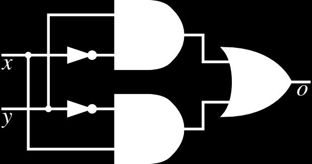
 Boolean Algebra and Logic Gates") Lecture (05) Boolean Algebra and Logic Gates By: Dr. Ahmed ElShafee ١ Minterms and Maxterms consider two binary variables x and y combined with an AND operation. Since eachv ariable may appear in either
Lecture (05) Boolean Algebra and Logic Gates By: Dr. Ahmed ElShafee ١ Minterms and Maxterms consider two binary variables x and y combined with an AND operation. Since eachv ariable may appear in either
Chap-2 Boolean Algebra
 Chap-2 Boolean Algebra Contents: My name Outline: My position, contact Basic information theorem and postulate of Boolean Algebra. or project description Boolean Algebra. Canonical and Standard form. Digital
3. The high voltage level of a digital signal in positive logic is : a) 1 b) 0 c) either 1 or 0
 1 b) 0 c) either 1 or 0") 1. The number of level in a digital signal is: a) one b) two c) four d) ten 2. A pure sine wave is : a) a digital signal b) analog signal c) can be digital or analog signal d) neither digital nor analog
1. The number of level in a digital signal is: a) one b) two c) four d) ten 2. A pure sine wave is : a) a digital signal b) analog signal c) can be digital or analog signal d) neither digital nor analog
CONTENTS CHAPTER 1: NUMBER SYSTEM. Foreword...(vii) Preface... (ix) Acknowledgement... (xi) About the Author...(xxiii)
 Preface... (ix) Acknowledgement... (xi) About the Author...(xxiii)") CONTENTS Foreword...(vii) Preface... (ix) Acknowledgement... (xi) About the Author...(xxiii) CHAPTER 1: NUMBER SYSTEM 1.1 Digital Electronics... 1 1.1.1 Introduction... 1 1.1.2 Advantages of Digital Systems...
CONTENTS Foreword...(vii) Preface... (ix) Acknowledgement... (xi) About the Author...(xxiii) CHAPTER 1: NUMBER SYSTEM 1.1 Digital Electronics... 1 1.1.1 Introduction... 1 1.1.2 Advantages of Digital Systems...
Memory and Programmable Logic
 Memory and Programmable Logic Memory units allow us to store and/or retrieve information Essentially look-up tables Good for storing data, not for function implementation Programmable logic device (PLD),
END-TERM EXAMINATION
 (Please Write your Exam Roll No. immediately) END-TERM EXAMINATION DECEMBER 2006 Exam. Roll No... Exam Series code: 100919DEC06200963 Paper Code: MCA-103 Subject: Digital Electronics Time: 3 Hours Maximum
Presentation 4: Programmable Combinational Devices
 Presentation 4: Programmable Combinational Devices Asst. Prof Dr. Ahmet ÖZKURT DEUEEE Based on the Presentation by Prof. Kim, Young Ho Dept. of Information Computer Engineering E-mail : yhkim@hyowon.cs.pusan.ac.kr
VALLIAMMAI ENGINEERING COLLEGE. SRM Nagar, Kattankulathur DEPARTMENT OF ELECTRONICS AND COMMUNICATION ENGINEERING EC6302 DIGITAL ELECTRONICS
 VALLIAMMAI ENGINEERING COLLEGE SRM Nagar, Kattankulathur-603 203 DEPARTMENT OF ELECTRONICS AND COMMUNICATION ENGINEERING EC6302 DIGITAL ELECTRONICS YEAR / SEMESTER: II / III ACADEMIC YEAR: 2015-2016 (ODD
R10. II B. Tech I Semester, Supplementary Examinations, May
 SET - 1 1. a) Convert the following decimal numbers into an equivalent binary numbers. i) 53.625 ii) 4097.188 iii) 167 iv) 0.4475 b) Add the following numbers using 2 s complement method. i) -48 and +31
Programmable Logic Devices UNIT II DIGITAL SYSTEM DESIGN
 Programmable Logic Devices UNIT II DIGITAL SYSTEM DESIGN 2 3 4 5 6 7 8 9 2 3 4 5 6 7 8 9 2 Implementation in Sequential Logic 2 PAL Logic Implementation Design Example: BCD to Gray Code Converter A B
Injntu.com Injntu.com Injntu.com R16
 1. a) What are the three methods of obtaining the 2 s complement of a given binary (3M) number? b) What do you mean by K-map? Name it advantages and disadvantages. (3M) c) Distinguish between a half-adder
HANSABA COLLEGE OF ENGINEERING & TECHNOLOGY (098) SUBJECT: DIGITAL ELECTRONICS ( ) Assignment
 SUBJECT: DIGITAL ELECTRONICS ( ) Assignment") Assignment 1. What is multiplexer? With logic circuit and function table explain the working of 4 to 1 line multiplexer. 2. Implement following Boolean function using 8: 1 multiplexer. F(A,B,C,D) = (2,3,5,7,8,9,12,13,14,15)
Assignment 1. What is multiplexer? With logic circuit and function table explain the working of 4 to 1 line multiplexer. 2. Implement following Boolean function using 8: 1 multiplexer. F(A,B,C,D) = (2,3,5,7,8,9,12,13,14,15)
Code No: R Set No. 1
 Code No: R059210504 Set No. 1 II B.Tech I Semester Regular Examinations, November 2006 DIGITAL LOGIC DESIGN ( Common to Computer Science & Engineering, Information Technology and Computer Science & Systems
Digital Logic Design Exercises. Assignment 1
 Assignment 1 For Exercises 1-5, match the following numbers with their definition A Number Natural number C Integer number D Negative number E Rational number 1 A unit of an abstract mathematical system
Chapter 13 Programmable Logic Device Architectures
 Chapter 13 Programmable Logic Device Architectures Chapter 13 Objectives Selected areas covered in this chapter: Describing different categories of digital system devices. Describing different types of
COLLEGE OF ENGINEERING DEPARTMENT OF ELECTRICAL AND ELECTRONICS ENGINEERING QUESTION BANK SUBJECT CODE & NAME: EC 1312 DIGITAL LOGIC CIRCUITS UNIT I
 KINGS COLLEGE OF ENGINEERING DEPARTMENT OF ELECTRICAL AND ELECTRONICS ENGINEERING QUESTION BANK SUBJECT CODE & NAME: EC 1312 DIGITAL LOGIC CIRCUITS YEAR / SEM: III / V UNIT I NUMBER SYSTEM & BOOLEAN ALGEBRA
QUESTION BANK FOR TEST
 CSCI 2121 Computer Organization and Assembly Language PRACTICE QUESTION BANK FOR TEST 1 Note: This represents a sample set. Please study all the topics from the lecture notes. Question 1. Multiple Choice
Programmable Logic Devices (PLDs)
") Programmable Logic Devices (PLDs) 212: Digital Design I, week 13 PLDs basically store binary information in a volatile/nonvolatile device. Data is specified by designer and physically inserted (Programmed)
Programmable Logic Devices (PLDs) 212: Digital Design I, week 13 PLDs basically store binary information in a volatile/nonvolatile device. Data is specified by designer and physically inserted (Programmed)
SHRI ANGALAMMAN COLLEGE OF ENGINEERING. (An ISO 9001:2008 Certified Institution) SIRUGANOOR, TIRUCHIRAPPALLI
 SIRUGANOOR, TIRUCHIRAPPALLI") SHRI ANGALAMMAN COLLEGE OF ENGINEERING AND TECHNOLOGY (An ISO 9001:2008 Certified Institution) SIRUGANOOR, TIRUCHIRAPPALLI 621 105 DEPARTMENT OF ELECTRONICS AND COMMUNICATION ENGINEERING EC1201 DIGITAL
SHRI ANGALAMMAN COLLEGE OF ENGINEERING AND TECHNOLOGY (An ISO 9001:2008 Certified Institution) SIRUGANOOR, TIRUCHIRAPPALLI 621 105 DEPARTMENT OF ELECTRONICS AND COMMUNICATION ENGINEERING EC1201 DIGITAL
Very Large Scale Integration (VLSI)
") Very Large Scale Integration (VLSI) Lecture 6 Dr. Ahmed H. Madian Ah_madian@hotmail.com Dr. Ahmed H. Madian-VLSI 1 Contents FPGA Technology Programmable logic Cell (PLC) Mux-based cells Look up table PLA
Very Large Scale Integration (VLSI) Lecture 6 Dr. Ahmed H. Madian Ah_madian@hotmail.com Dr. Ahmed H. Madian-VLSI 1 Contents FPGA Technology Programmable logic Cell (PLC) Mux-based cells Look up table PLA
Topics. Midterm Finish Chapter 7
 Lecture 9 Topics Midterm Finish Chapter 7 ROM (review) Memory device in which permanent binary information is stored. Example: 32 x 8 ROM Five input lines (2 5 = 32) 32 outputs, each representing a memory
Memory and Programmable Logic
 Digital Circuit Design and Language Memory and Programmable Logic Chang, Ik Joon Kyunghee University Memory Classification based on functionality ROM : Read-Only Memory RWM : Read-Write Memory RWM NVRWM
1. Mark the correct statement(s)
") 1. Mark the correct statement(s) 1.1 A theorem in Boolean algebra: a) Can easily be proved by e.g. logic induction b) Is a logical statement that is assumed to be true, c) Can be contradicted by another
1. Mark the correct statement(s) 1.1 A theorem in Boolean algebra: a) Can easily be proved by e.g. logic induction b) Is a logical statement that is assumed to be true, c) Can be contradicted by another
Henry Lin, Department of Electrical and Computer Engineering, California State University, Bakersfield Lecture 7 (Digital Logic) July 24 th, 2012
 July 24 th, 2012") Henry Lin, Department of Electrical and Computer Engineering, California State University, Bakersfield Lecture 7 (Digital Logic) July 24 th, 2012 1 Digital vs Analog Digital signals are binary; analog
Henry Lin, Department of Electrical and Computer Engineering, California State University, Bakersfield Lecture 7 (Digital Logic) July 24 th, 2012 1 Digital vs Analog Digital signals are binary; analog
Model EXAM Question Bank
 VELAMMAL COLLEGE OF ENGINEERING AND TECHNOLOGY, MADURAI Department of Information Technology Model Exam -1 1. List the main difference between PLA and PAL. PLA: Both AND and OR arrays are programmable
PROGRAMMABLE MODULES SPECIFICATION OF PROGRAMMABLE COMBINATIONAL AND SEQUENTIAL MODULES
 PROGRAMMABLE MODULES SPECIFICATION OF PROGRAMMABLE COMBINATIONAL AND SEQUENTIAL MODULES. psa. rom. fpga THE WAY THE MODULES ARE PROGRAMMED NETWORKS OF PROGRAMMABLE MODULES EXAMPLES OF USES Programmable
Boolean Algebra and Logic Gates
 Boolean Algebra and Logic Gates Binary logic is used in all of today's digital computers and devices Cost of the circuits is an important factor Finding simpler and cheaper but equivalent circuits can
Code No: 07A3EC03 Set No. 1
 Code No: 07A3EC03 Set No. 1 II B.Tech I Semester Regular Examinations, November 2008 SWITCHING THEORY AND LOGIC DESIGN ( Common to Electrical & Electronic Engineering, Electronics & Instrumentation Engineering,
Unit 6 1.Random Access Memory (RAM) Chapter 3 Combinational Logic Design 2.Programmable Logic
 Chapter 3 Combinational Logic Design 2.Programmable Logic") EE 200: Digital Logic Circuit Design Dr Radwan E Abdel-Aal, COE Unit 6.Random Access Memory (RAM) Chapter 3 Combinational Logic Design 2. Logic Logic and Computer Design Fundamentals Part Implementation
EE 200: Digital Logic Circuit Design Dr Radwan E Abdel-Aal, COE Unit 6.Random Access Memory (RAM) Chapter 3 Combinational Logic Design 2. Logic Logic and Computer Design Fundamentals Part Implementation
Chapter 2 Logic Gates and Introduction to Computer Architecture
 Chapter 2 Logic Gates and Introduction to Computer Architecture 2.1 Introduction The basic components of an Integrated Circuit (IC) is logic gates which made of transistors, in digital system there are
(ii) Simplify and implement the following SOP function using NOR gates:
 Simplify and implement the following SOP function using NOR gates:") DHANALAKSHMI COLLEGE OF ENGINEERING DEPARTMENT OF ELECTRONICS AND COMMUNICATION ENGINEERING EE6301 DIGITAL LOGIC CIRCUITS UNIT I NUMBER SYSTEMS AND DIGITAL LOGIC FAMILIES PART A 1. How can an OR gate be
DHANALAKSHMI COLLEGE OF ENGINEERING DEPARTMENT OF ELECTRONICS AND COMMUNICATION ENGINEERING EE6301 DIGITAL LOGIC CIRCUITS UNIT I NUMBER SYSTEMS AND DIGITAL LOGIC FAMILIES PART A 1. How can an OR gate be
Principles of Digital Techniques PDT (17320) Assignment No State advantages of digital system over analog system.
 Assignment No State advantages of digital system over analog system.") Assignment No. 1 1. State advantages of digital system over analog system. 2. Convert following numbers a. (138.56) 10 = (?) 2 = (?) 8 = (?) 16 b. (1110011.011) 2 = (?) 10 = (?) 8 = (?) 16 c. (3004.06)
Assignment No. 1 1. State advantages of digital system over analog system. 2. Convert following numbers a. (138.56) 10 = (?) 2 = (?) 8 = (?) 16 b. (1110011.011) 2 = (?) 10 = (?) 8 = (?) 16 c. (3004.06)
EECS 150 Homework 7 Solutions Fall (a) 4.3 The functions for the 7 segment display decoder given in Section 4.3 are:
 4.3 The functions for the 7 segment display decoder given in Section 4.3 are:") Problem 1: CLD2 Problems. (a) 4.3 The functions for the 7 segment display decoder given in Section 4.3 are: C 0 = A + BD + C + BD C 1 = A + CD + CD + B C 2 = A + B + C + D C 3 = BD + CD + BCD + BC C 4
Problem 1: CLD2 Problems. (a) 4.3 The functions for the 7 segment display decoder given in Section 4.3 are: C 0 = A + BD + C + BD C 1 = A + CD + CD + B C 2 = A + B + C + D C 3 = BD + CD + BCD + BC C 4
Scheme G. Sample Test Paper-I
 Sample Test Paper-I Marks : 25 Times:1 Hour 1. All questions are compulsory. 2. Illustrate your answers with neat sketches wherever necessary. 3. Figures to the right indicate full marks. 4. Assume suitable
MGU-BCA-205- Second Sem- Core VI- Fundamentals of Digital Systems- MCQ s. 2. Why the decimal number system is also called as positional number system?
 MGU-BCA-205- Second Sem- Core VI- Fundamentals of Digital Systems- MCQ s Unit-1 Number Systems 1. What does a decimal number represents? A. Quality B. Quantity C. Position D. None of the above 2. Why the
Lecture 21: Combinational Circuits. Integrated Circuits. Integrated Circuits, cont. Integrated Circuits Combinational Circuits
 Lecture 21: Combinational Circuits Integrated Circuits Combinational Circuits Multiplexer Demultiplexer Decoder Adders ALU Integrated Circuits Circuits use modules that contain multiple gates packaged
DIRECTORATE OF DISTANCE EDUCATION COMPUTER ORGANIZATION AND ARCHITECTURE/INTRODUCTION TO COMPUTER ORGANIZATION AND ARCHITECTURE
 www.lpude.in DIRECTORATE OF DISTANCE EDUCATION COMPUTER ORGANIZATION AND ARCHITECTURE/INTRODUCTION TO COMPUTER ORGANIZATION AND ARCHITECTURE Copyright 2012 Lovely Professional University All rights reserved
Introduction to Programmable Logic Devices (Class 7.2 2/28/2013)
") Introduction to Programmable Logic Devices (Class 7.2 2/28/2013) CSE 2441 Introduction to Digital Logic Spring 2013 Instructor Bill Carroll, Professor of CSE Today s Topics Complexity issues Implementation
Introduction to Programmable Logic Devices (Class 7.2 2/28/2013) CSE 2441 Introduction to Digital Logic Spring 2013 Instructor Bill Carroll, Professor of CSE Today s Topics Complexity issues Implementation
R a) Simplify the logic functions from binary to seven segment display code converter (8M) b) Simplify the following using Tabular method
 Simplify the logic functions from binary to seven segment display code converter (8M) b) Simplify the following using Tabular method") SET - 1 1. a) Convert the decimal number 250.5 to base 3, base 4 b) Write and prove de-morgan laws c) Implement two input EX-OR gate from 2 to 1 multiplexer (3M) d) Write the demerits of PROM (3M) e) What
SET - 1 1. a) Convert the decimal number 250.5 to base 3, base 4 b) Write and prove de-morgan laws c) Implement two input EX-OR gate from 2 to 1 multiplexer (3M) d) Write the demerits of PROM (3M) e) What
Chapter 4: Combinational Logic
 Chapter 4: Combinational Logic Combinational Circuit Design Analysis Procedure (Find out nature of O/P) Boolean Expression Approach Truth Table Approach Design Procedure Example : BCD to Excess-3 code
Lecture 7. Standard ICs FPGA (Field Programmable Gate Array) VHDL (Very-high-speed integrated circuits. Hardware Description Language)
 VHDL (Very-high-speed integrated circuits. Hardware Description Language)") Standard ICs FPGA (Field Programmable Gate Array) VHDL (Very-high-speed integrated circuits Hardware Description Language) 1 Standard ICs PLD: Programmable Logic Device CPLD: Complex PLD FPGA: Field Programmable
Standard ICs FPGA (Field Programmable Gate Array) VHDL (Very-high-speed integrated circuits Hardware Description Language) 1 Standard ICs PLD: Programmable Logic Device CPLD: Complex PLD FPGA: Field Programmable
EECS150, Fall 2004, Midterm 1, Prof. Culler. Problem 1 (15 points) 1.a. Circle the gate-level circuits that DO NOT implement a Boolean AND function.
 1.a. Circle the gate-level circuits that DO NOT implement a Boolean AND function.") Problem 1 (15 points) 1.a. Circle the gate-level circuits that DO NOT implement a Boolean AND function. 1.b. Show that a 2-to-1 MUX is universal (i.e. that any Boolean expression can be implemented with
Problem 1 (15 points) 1.a. Circle the gate-level circuits that DO NOT implement a Boolean AND function. 1.b. Show that a 2-to-1 MUX is universal (i.e. that any Boolean expression can be implemented with
UNIT - V MEMORY P.VIDYA SAGAR ( ASSOCIATE PROFESSOR) Department of Electronics and Communication Engineering, VBIT
 Department of Electronics and Communication Engineering, VBIT") UNIT - V MEMORY P.VIDYA SAGAR ( ASSOCIATE PROFESSOR) contents Memory: Introduction, Random-Access memory, Memory decoding, ROM, Programmable Logic Array, Programmable Array Logic, Sequential programmable
UNIT - V MEMORY P.VIDYA SAGAR ( ASSOCIATE PROFESSOR) contents Memory: Introduction, Random-Access memory, Memory decoding, ROM, Programmable Logic Array, Programmable Array Logic, Sequential programmable
Purdue IMPACT 2015 Edition by D. G. Meyer. Introduction to Digital System Design. Module 2 Combinational Logic Circuits
 Purdue IMPACT 25 Edition by D. G. Meyer Introduction to Digital System Design Module 2 Combinational Logic Circuits Glossary of Common Terms DISCRETE LOGIC a circuit constructed using small-scale integrated
Date Performed: Marks Obtained: /10. Group Members (ID):. Experiment # 09 MULTIPLEXERS
:. Experiment # 09 MULTIPLEXERS") Name: Instructor: Engr. Date Performed: Marks Obtained: /10 Group Members (ID):. Checked By: Date: Experiment # 09 MULTIPLEXERS OBJECTIVES: To experimentally verify the proper operation of a multiplexer.
Name: Instructor: Engr. Date Performed: Marks Obtained: /10 Group Members (ID):. Checked By: Date: Experiment # 09 MULTIPLEXERS OBJECTIVES: To experimentally verify the proper operation of a multiplexer.
LECTURE 4. Logic Design
 LECTURE 4 Logic Design LOGIC DESIGN The language of the machine is binary that is, sequences of 1 s and 0 s. But why? At the hardware level, computers are streams of signals. These signals only have two
MEMORY AND PROGRAMMABLE LOGIC
 MEMORY AND PROGRAMMABLE LOGIC Memory is a device where we can store and retrieve information It can execute a read and a write Programmable Logic is a device where we can store and retrieve information
Outline. Field Programmable Gate Arrays. Programming Technologies Architectures. Programming Interfaces. Historical perspective
 Outline Field Programmable Gate Arrays Historical perspective Programming Technologies Architectures PALs, PLDs,, and CPLDs FPGAs Programmable logic Interconnect network I/O buffers Specialized cores Programming
SUBJECT CODE: IT T35 DIGITAL SYSTEM DESIGN YEAR / SEM : 2 / 3
 UNIT - I PART A (2 Marks) 1. Using Demorgan s theorem convert the following Boolean expression to an equivalent expression that has only OR and complement operations. Show the function can be implemented
Code No: R Set No. 1
 Code No: R059210504 Set No. 1 II B.Tech I Semester Supplementary Examinations, February 2007 DIGITAL LOGIC DESIGN ( Common to Computer Science & Engineering, Information Technology and Computer Science
INSTITUTE OF AERONAUTICAL ENGINEERING (Autonomous) Dundigal, Hyderabad
 Dundigal, Hyderabad") INSTITUTE OF AERONAUTICAL ENGINEERING (Autonomous) Dundigal, Hyderabad - 500 043 COMPUTER SCIENCE AND ENGINEERING TUTORIAL QUESTION BANK Name : DIGITAL LOGIC DESISN Code : AEC020 Class : B Tech III Semester
INSTITUTE OF AERONAUTICAL ENGINEERING (Autonomous) Dundigal, Hyderabad - 500 043 COMPUTER SCIENCE AND ENGINEERING TUTORIAL QUESTION BANK Name : DIGITAL LOGIC DESISN Code : AEC020 Class : B Tech III Semester
B.Tech II Year I Semester (R13) Regular Examinations December 2014 DIGITAL LOGIC DESIGN
 Regular Examinations December 2014 DIGITAL LOGIC DESIGN") B.Tech II Year I Semester () Regular Examinations December 2014 (Common to IT and CSE) (a) If 1010 2 + 10 2 = X 10, then X is ----- Write the first 9 decimal digits in base 3. (c) What is meant by don
B.Tech II Year I Semester () Regular Examinations December 2014 (Common to IT and CSE) (a) If 1010 2 + 10 2 = X 10, then X is ----- Write the first 9 decimal digits in base 3. (c) What is meant by don
Programmable Memory Blocks Supporting Content-Addressable Memory
 Programmable Memory Blocks Supporting Content-Addressable Memory Frank Heile, Andrew Leaver, Kerry Veenstra Altera 0 Innovation Dr San Jose, CA 95 USA (408) 544-7000 {frank, aleaver, kerry}@altera.com
KINGS COLLEGE OF ENGINEERING DEPARTMENT OF ELECTRICAL AND ELECTRONICS ENGINEERING QUESTION BANK NAME OF THE SUBJECT: EE 2255 DIGITAL LOGIC CIRCUITS
 KINGS COLLEGE OF ENGINEERING DEPARTMENT OF ELECTRICAL AND ELECTRONICS ENGINEERING QUESTION BANK NAME OF THE SUBJECT: EE 2255 DIGITAL LOGIC CIRCUITS YEAR / SEM: II / IV UNIT I BOOLEAN ALGEBRA AND COMBINATIONAL
ELCT 912: Advanced Embedded Systems
 Advanced Embedded Systems Lecture 2: Memory and Programmable Logic Dr. Mohamed Abd El Ghany, Memory Random Access Memory (RAM) Can be read and written Static Random Access Memory (SRAM) Data stored so
Boolean Algebra. BME208 Logic Circuits Yalçın İŞLER
 Boolean Algebra BME28 Logic Circuits Yalçın İŞLER islerya@yahoo.com http://me.islerya.com 5 Boolean Algebra /2 A set of elements B There exist at least two elements x, y B s. t. x y Binary operators: +
Digital Design with FPGAs. By Neeraj Kulkarni
 Digital Design with FPGAs By Neeraj Kulkarni Some Basic Electronics Basic Elements: Gates: And, Or, Nor, Nand, Xor.. Memory elements: Flip Flops, Registers.. Techniques to design a circuit using basic
Review: Chip Design Styles
 MPT-50 Introduction to omputer Design SFU, Harbour entre, Spring 007 Lecture 9: Feb. 6, 007 Programmable Logic Devices (PLDs) - Read Only Memory (ROM) - Programmable Array Logic (PAL) - Programmable Logic
Hours / 100 Marks Seat No.
 17333 13141 3 Hours / 100 Seat No. Instructions (1) All Questions are Compulsory. (2) Answer each next main Question on a new page. (3) Illustrate your answers with neat sketches wherever necessary. (4)
DIGITAL SYSTEM FUNDAMENTALS (ECE421) DIGITAL ELECTRONICS FUNDAMENTAL (ECE4220. PROGRAMMABLE LOGIC DEVICES (PLDs)
 DIGITAL ELECTRONICS FUNDAMENTAL (ECE4220. PROGRAMMABLE LOGIC DEVICES (PLDs)") COURSE / CODE DIGITAL SYSTEM FUNDAMENTALS (ECE421) DIGITAL ELECTRONICS FUNDAMENTAL (ECE4220 PROGRAMMABLE LOGIC DEVICES (PLDs) A PLD, or programmable logic device, is an electronic component that is used
COURSE / CODE DIGITAL SYSTEM FUNDAMENTALS (ECE421) DIGITAL ELECTRONICS FUNDAMENTAL (ECE4220 PROGRAMMABLE LOGIC DEVICES (PLDs) A PLD, or programmable logic device, is an electronic component that is used
FPGA for Complex System Implementation. National Chiao Tung University Chun-Jen Tsai 04/14/2011
 FPGA for Complex System Implementation National Chiao Tung University Chun-Jen Tsai 04/14/2011 About FPGA FPGA was invented by Ross Freeman in 1989 SRAM-based FPGA properties Standard parts Allowing multi-level
NADAR SARASWATHI COLLEGE OF ENGINEERING AND TECHNOLOGY Vadapudupatti, Theni
 NADAR SARASWATHI COLLEGE OF ENGINEERING AND TECHNOLOGY Vadapudupatti, Theni-625531 Question Bank for the Units I to V SEMESTER BRANCH SUB CODE 3rd Semester B.E. / B.Tech. Electrical and Electronics Engineering
DIGITAL ELECTRONICS. Vayu Education of India
 DIGITAL ELECTRONICS ARUN RANA Assistant Professor Department of Electronics & Communication Engineering Doon Valley Institute of Engineering & Technology Karnal, Haryana (An ISO 9001:2008 ) Vayu Education
PART B. 3. Minimize the following function using K-map and also verify through tabulation method. F (A, B, C, D) = +d (0, 3, 6, 10).
 = +d (0, 3, 6, 10).") II B. Tech II Semester Regular Examinations, May/June 2015 SWITCHING THEORY AND LOGIC DESIGN (Com. to EEE, ECE, ECC, EIE.) Time: 3 hours Max. Marks: 70 Note: 1. Question Paper consists of two parts (Part-A
II B. Tech II Semester Regular Examinations, May/June 2015 SWITCHING THEORY AND LOGIC DESIGN (Com. to EEE, ECE, ECC, EIE.) Time: 3 hours Max. Marks: 70 Note: 1. Question Paper consists of two parts (Part-A
KING FAHD UNIVERSITY OF PETROLEUM & MINERALS COMPUTER ENGINEERING DEPARTMENT
 KING FAHD UNIVERSITY OF PETROLEUM & MINERALS COMPUTER ENGINEERING DEPARTMENT COE 202: Digital Logic Design Term 162 (Spring 2017) Instructor: Dr. Abdulaziz Barnawi Class time: U.T.R.: 11:00-11:50AM Class
BHARATHIDASAN ENGINEERING COLLEGE Degree / Branch : B.E./ECE Year / Sem : II/ III Sub.Code / Name : EC6302/DIGITAL ELECTRONICS
 BHARATHIDASAN ENGINEERING COLLEGE Degree / Branch : B.E./ECE Year / Sem : II/ III Sub.Code / Name : EC6302/DIGITAL ELECTRONICS FREQUENTLY ASKED QUESTIONS UNIT I MINIMIZATION TECHNIQUES AND LOGIC GATES
BUILDING BLOCKS OF A BASIC MICROPROCESSOR. Part 1 PowerPoint Format of Lecture 3 of Book
 BUILDING BLOCKS OF A BASIC MICROPROCESSOR Part PowerPoint Format of Lecture 3 of Book Decoder Tri-state device Full adder, full subtractor Arithmetic Logic Unit (ALU) Memories Example showing how to write
Chapter 2. Boolean Algebra and Logic Gates
 Chapter 2. Boolean Algebra and Logic Gates Tong In Oh 1 Basic Definitions 2 3 2.3 Axiomatic Definition of Boolean Algebra Boolean algebra: Algebraic structure defined by a set of elements, B, together
COPYRIGHTED MATERIAL INDEX
 INDEX Absorption law, 31, 38 Acyclic graph, 35 tree, 36 Addition operators, in VHDL (VHSIC hardware description language), 192 Algebraic division, 105 AND gate, 48 49 Antisymmetric, 34 Applicable input
CHAPTER - 2 : DESIGN OF ARITHMETIC CIRCUITS
 Contents i SYLLABUS osmania university UNIT - I CHAPTER - 1 : BASIC VERILOG HDL Introduction to HDLs, Overview of Digital Design With Verilog HDL, Basic Concepts, Data Types, System Tasks and Compiler
Programmable Logic Devices (PLDs) >Programmable Array Logic (PALs) >Programmable Logic Arrays (PLAs) PAL/GAL 16V8 CPLD: Altera s MAX 3064 & MAX V
 >Programmable Array Logic (PALs) >Programmable Logic Arrays (PLAs) PAL/GAL 16V8 CPLD: Altera s MAX 3064 & MAX V") Menu Look into my... Programmable Logic Devices (PLDs) >Programmable Array Logic (PALs) >Programmable Logic Arrays (PLAs) PAL/GAL 16V8 CPLD: Altera s MAX 3064 & MAX V Read Roth: Sections 9.6-9.8 (Sections
Menu Look into my... Programmable Logic Devices (PLDs) >Programmable Array Logic (PALs) >Programmable Logic Arrays (PLAs) PAL/GAL 16V8 CPLD: Altera s MAX 3064 & MAX V Read Roth: Sections 9.6-9.8 (Sections
PINE TRAINING ACADEMY
 PINE TRAINING ACADEMY Course Module A d d r e s s D - 5 5 7, G o v i n d p u r a m, G h a z i a b a d, U. P., 2 0 1 0 1 3, I n d i a Digital Logic System Design using Gates/Verilog or VHDL and Implementation
Digital Design Using Digilent FPGA Boards -- Verilog / Active-HDL Edition
 Digital Design Using Digilent FPGA Boards -- Verilog / Active-HDL Edition Table of Contents 1. Introduction to Digital Logic 1 1.1 Background 1 1.2 Digital Logic 5 1.3 Verilog 8 2. Basic Logic Gates 9
Programmable Logic Devices
 Programmable Logic Devices INTRODUCTION A programmable logic device or PLD is an electronic component used to build reconfigurable digital circuits. Unlike a logic gate, which has a fixed function, a PLD
EET2411 DIGITAL ELECTRONICS. A device or electrical circuit used to store a single bit (0 or 1) Ex. FF.
 Ex. FF.") Chapter 12 - Memory Devices Digital information is easily stored Commonly used memory devices and systems will be examined Flip flops Registers VLSI and LSI memory devices The difference between main memory
Chapter 12 - Memory Devices Digital information is easily stored Commonly used memory devices and systems will be examined Flip flops Registers VLSI and LSI memory devices The difference between main memory
R07
 www..com www..com SET - 1 II B. Tech I Semester Supplementary Examinations May 2013 SWITCHING THEORY AND LOGIC DESIGN (Com. to EEE, EIE, BME, ECC) Time: 3 hours Max. Marks: 80 Answer any FIVE Questions
(Refer Slide Time: 00:01:53)
") Digital Circuits and Systems Prof. S. Srinivasan Department of Electrical Engineering Indian Institute of Technology Madras Lecture - 36 Design of Circuits using MSI Sequential Blocks (Refer Slide Time:
Digital Circuits and Systems Prof. S. Srinivasan Department of Electrical Engineering Indian Institute of Technology Madras Lecture - 36 Design of Circuits using MSI Sequential Blocks (Refer Slide Time:
Section 6. Memory Components Chapter 5.7, 5.8 Physical Implementations Chapter 7 Programmable Processors Chapter 8
 Section 6 Memory Components Chapter 5.7, 5.8 Physical Implementations Chapter 7 Programmable Processors Chapter 8 Types of memory Two major types of memory Volatile When power to the device is removed
II/IV B.Tech (Regular/Supplementary) DEGREE EXAMINATION. Answer ONE question from each unit.
 DEGREE EXAMINATION. Answer ONE question from each unit.") Hall Ticket Number: 14CS IT303 November, 2017 Third Semester Time: Three Hours Answer Question No.1 compulsorily. II/IV B.Tech (Regular/Supplementary) DEGREE EXAMINATION Common for CSE & IT Digital Logic
Hall Ticket Number: 14CS IT303 November, 2017 Third Semester Time: Three Hours Answer Question No.1 compulsorily. II/IV B.Tech (Regular/Supplementary) DEGREE EXAMINATION Common for CSE & IT Digital Logic
INSTITUTE OF AERONAUTICAL ENGINEERING (Autonomous) Dundigal, Hyderabad
 Dundigal, Hyderabad") INSTITUTE OF AERONAUTICAL ENGINEERING (Autonomous) Dundigal, Hyderabad - 500043 Course Name : DIGITAL LOGIC DESISN Course Code : AEC020 Class : B Tech III Semester Branch : CSE Academic Year : 2018 2019
INSTITUTE OF AERONAUTICAL ENGINEERING (Autonomous) Dundigal, Hyderabad - 500043 Course Name : DIGITAL LOGIC DESISN Course Code : AEC020 Class : B Tech III Semester Branch : CSE Academic Year : 2018 2019
Digital Systems Design with PLDs and FPGAs Kuruvilla Varghese Department of Electronic Systems Engineering Indian Institute of Science Bangalore
 Digital Systems Design with PLDs and FPGAs Kuruvilla Varghese Department of Electronic Systems Engineering Indian Institute of Science Bangalore Lecture-32 Simple PLDs So welcome to just lecture on programmable
Combinational Circuits
 Combinational Circuits Jason Filippou CMSC250 @ UMCP 06-02-2016 ason Filippou (CMSC250 @ UMCP) Circuits 06-02-2016 1 / 1 Outline ason Filippou (CMSC250 @ UMCP) Circuits 06-02-2016 2 / 1 Hardware design
VALLIAMMAI ENGINEERING COLLEGE
 VALLIAMMAI ENGINEERING COLLEGE SRM Nagar, Kattankulathur 603 203 DEPARTMENT OF INFORMATION TECHNOLOGY & COMPUTER SCIENCE AND ENGINEERING QUESTION BANK II SEMESTER CS6201- DIGITAL PRINCIPLE AND SYSTEM DESIGN
UNIT V (PROGRAMMABLE LOGIC DEVICES)
") UNIT V (PROGRAMMABLE LOGIC DEVICES) Introduction There are two types of memories that are used in digital systems: Random-access memory(ram): perform both the write and read operations. Read-only memory(rom):
UNIT V (PROGRAMMABLE LOGIC DEVICES) Introduction There are two types of memories that are used in digital systems: Random-access memory(ram): perform both the write and read operations. Read-only memory(rom):
FPGA: What? Why? Marco D. Santambrogio
 FPGA: What? Why? Marco D. Santambrogio marco.santambrogio@polimi.it 2 Reconfigurable Hardware Reconfigurable computing is intended to fill the gap between hardware and software, achieving potentially much
SIDDHARTH GROUP OF INSTITUTIONS :: PUTTUR Siddharth Nagar, Narayanavanam Road QUESTION BANK (DESCRIPTIVE)
") SIDDHARTH GROUP OF INSTITUTIONS :: PUTTUR Siddharth Nagar, Narayanavanam Road 517583 QUESTION BANK (DESCRIPTIVE) Subject with Code : STLD(16EC402) Year & Sem: II-B.Tech & I-Sem Course & Branch: B.Tech
SIDDHARTH GROUP OF INSTITUTIONS :: PUTTUR Siddharth Nagar, Narayanavanam Road 517583 QUESTION BANK (DESCRIPTIVE) Subject with Code : STLD(16EC402) Year & Sem: II-B.Tech & I-Sem Course & Branch: B.Tech
Course Batch Semester Subject Code Subject Name. B.E-Marine Engineering B.E- ME-16 III UBEE307 Integrated Circuits
 Course Batch Semester Subject Code Subject Name B.E-Marine Engineering B.E- ME-16 III UBEE307 Integrated Circuits Part-A 1 Define De-Morgan's theorem. 2 Convert the following hexadecimal number to decimal
ECE/Comp Sci 352 Digital Systems Fundamentals Kewal K. Saluja and Yu Hen Hu Spring Logic and Computer Design Fundamentals.
 University of Wisconsin - Madison ECE/Comp Sci 352 Digital Systems Fundamentals Kewal K. Saluja and Yu Hen Hu Spring 2002 Chapter 6 Part 2 Memories & Programmable Logic Devices Originals by: Charles R.
Combinational Logic II
 Combinational Logic II Ranga Rodrigo July 26, 2009 1 Binary Adder-Subtractor Digital computers perform variety of information processing tasks. Among the functions encountered are the various arithmetic
Fig. 6-1 Conventional and Array Logic Symbols for OR Gate
 6- (a) Conventional symbol (b) Array logic symbol Fig. 6- Conventional and Array Logic Symbols for OR Gate 2 Prentice Hall, Inc. 6-2 k address lines Read n data input lines emory unit 2 k words n bits
Read-only memory Implementing logic with ROM Programmable logic devices Implementing logic with PLDs Static hazards
 Points Addressed in this Lecture Lecture 7: ROM Programmable Logic Devices Professor Peter Cheung Department of EEE, Imperial College London Read-only memory Implementing logic with ROM Programmable logic
Evolution of Implementation Technologies. ECE 4211/5211 Rapid Prototyping with FPGAs. Gate Array Technology (IBM s) Programmable Logic
 Programmable Logic") ECE 42/52 Rapid Prototyping with FPGAs Dr. Charlie Wang Department of Electrical and Computer Engineering University of Colorado at Colorado Springs Evolution of Implementation Technologies Discrete devices:
ECE 42/52 Rapid Prototyping with FPGAs Dr. Charlie Wang Department of Electrical and Computer Engineering University of Colorado at Colorado Springs Evolution of Implementation Technologies Discrete devices:
Altera FLEX 8000 Block Diagram
 Altera FLEX 8000 Block Diagram Figure from Altera technical literature FLEX 8000 chip contains 26 162 LABs Each LAB contains 8 Logic Elements (LEs), so a chip contains 208 1296 LEs, totaling 2,500 16,000
Follow-up question: now, comment on what each of these acronyms actually means, going beyond a mere recitation of the definition.
 Question 1 Define the following acronyms as they apply to digital logic circuits: ASIC PAL PLA PLD CPLD FPGA file 03041 Answer 1 ASIC: Application-Specific Integrated Circuit PAL: Programmable Array Logic
FPGA Design Challenge :Techkriti 14 Digital Design using Verilog Part 1
 FPGA Design Challenge :Techkriti 14 Digital Design using Verilog Part 1 Anurag Dwivedi Digital Design : Bottom Up Approach Basic Block - Gates Digital Design : Bottom Up Approach Gates -> Flip Flops Digital
DHANALAKSHMI SRINIVASAN COLLEGE OF ENGINEERING AND TECHNOLOGY
 DHANALAKSHMI SRINIVASAN COLLEGE OF ENGINEERING AND TECHNOLOGY Dept/Sem: II CSE/03 DEPARTMENT OF ECE CS8351 DIGITAL PRINCIPLES AND SYSTEM DESIGN UNIT I BOOLEAN ALGEBRA AND LOGIC GATES PART A 1. How many