MICROPROCESSOR AND MICROCONTROLLER
|
|
|
- Timothy Richards
- 6 years ago
- Views:
Transcription

1 A Course Material on By Mr. C.JAGADEESHWARAN ASSISTANT PROFESSOR DEPARTMENT OF ELECTRONICS & COMMUNICATION ENGINEERING SASURIE COLLEGE OF ENGINEERING VIJAYAMANGALAM
2 QUALITY CERTIFICATE This is to certify that the e-course material Subject Code Scubject Class : : Microprocessor and Microcontroller : III Year EEE being prepared by me and it meets the knowledge requirement of the university curriculum. Signature of the Author Name: Designation: C.Jagadeeshwaran Assistant Professor/ECE This is to certify that the course material being prepared by Mr. C.Jagadeeshwaran is of adequate quality. He has referred more than five books amont them minimum one is from aborad author. Signature of HD Name: S.Sriram
3 CONTENTS UNIT 885 & 886 PROCESSOR to Hardware Architecture of 885 Microprocessor Pin Diagram Memory Interfacing.3. Typical EPROM and Static RAM.3.2 Example for Memory Interfacing Timing Diagram.4. Machine cycles of Timing diagram for STA 526AH.4.3 Timing diagram for INR M Interrupts.5.Types of Interrupts Hardware Architecture of 885 Microprocessor 886-Minimum mode of operation.7. Minimum Mode Interface.7.2 Maximum Mode Interface I/O Ports UNIT 2 PROGRAMMING OF 885 PROCESSOR 25 to Instruction Format 2.. One-Byte Instructions 2..2 Two-Byte Instructions 2..3 Three-Byte Instructions The 885 Addressing Modes Instruction Set Classification 2.3. Data Transfer Croup Arithmetic Group Logical Group Branch Group Stack Instructions I/ instructions Machine Control instructions Sample Program Programming using Loop structure with Counting and Indexing Programming using subroutine Instructions Programming using Look up table UNIT 3 PERIPHERAL INTERFACING 37 to Programmable peripheral interface (8255) 3.. Architecture of Pin Diagram of Operational Modes of
4 Control Word Format Programmable Interrupt Controller (8259) 3.2. Features Pinout Block diagram 825 USART 3.3. Block Diagram of Control Words Status Word Programmable Keyboard/Display Interface Pinout Definition Block Diagram of Keyboard Interface of 8279 ADC Interfacing with 885 Microprocessor 3.5. Features Block Diagram of ADC 89 DAC Interfacing with 885 Microprocessor 3.6. DAC 8 Features Circuit Diagram of DAC 8 UNIT 4 85 MICRO CONTROLLER 6 to Architecture of Memory Organization 4..2 Interrupt Structure 4..3 Port Structure 4..4 Timer/Counter Instruction Format 4.2. One-Byte Instructions Two-Byte Instructions Three-Byte Instructions Addressing Modes of 85 Interrupt Structure 4.4. External Interrupt Handling Interrupt I/O Ports Timers 4.6.Timer SFR bit Time Mode (mode ) bit Time Mode (mode ) bit Time Mode (mode 2) Split Timer Mode (mode 3) Using Timers As Event Counters Serial Communication
5 UNIT 5 MICRO CONTROLLER PROGRAMMING & APPLICATIONS 7 to Arithmetic Instructions Logical Instructions Data Transfer Instructions that access the Internal Data Memory Data Transfer Instructions that access the External Data Memory Look up Tables Boolean Instructions Jump Instructions Interfacing Keyboard to 85 Microcontroller Program for Keyboard Interfacing with 85 Seven Segment Disply Interfacing with 85 LCD Interfacing Stepper Motor Interfacing Servo Motor 5.3. Controlling the Servo Motor Program Washing Machine Control 5.4. SCHEMATIC Working of Washing Machine
6 MICROPROCESSORS AND MICRO CONTROLLER L T P C 3 3 AIM To introduce Microprocessor Intel 885 and 886 and the Micro Controller 85 OBJECTIVES To study the Architecture of 885 & 886, 85 To study the addressing modes & instruction set of 885 & 85. To introduce the need & use of Interrupt structure 885 & 85. To develop skill in simple program writing for 85 & 885 and applications To introduce commonly used peripheral / interfacing ICs UNIT I 885 and 886 PROCESSOR 9 Hardware Architecture pintouts - Signals Memory interfacing I/O ports and data transfer concepts Timing Diagram Interrupt structure. UNIT II PROGRAMMING OF 885 PROCESSOR 9 Instruction format and addressing modes Assembly language format Data transfer, data manipulation & control instructions Programming: Loop structure with counting & Indexing - Look up table - Subroutine instructions - stack. UNIT III PERIPHERAL INTERFACING 9 Study of Architecture and programming of ICs: 8255 PPI, 8259 PIC, 825 USART, 8279 Key board display controller and 8253 Timer/ Counter Interfacing with A/D and D/A converter interfacing. UNIT IV 85 MICRO CONTROLLER 9 Functional block diagram - Instruction format and addressing modes Timing Diagram Interrupt structure Timer I/O ports Serial communication. UNIT V MICRO CONTROLLER PROGRAMMING & APPLICATIONS 9 Data Transfer, Manipulation, Control & I/O instructions Simple programming exercises key board and display interface Closed loop control of servo motor- stepper motor control - Washing Machine Control. TEXT BOOKS L = 45 T = 5 TOTAL : 6 PERIODS. Microprocessor and Microcontrollers, Krishna Kant Eastern Company Edition, Prentice Hall of India, New Delhi, Muhammad Ali Mazidi & Janice Gilli Mazidi, R.D.Kinely The 85 Micro Controller and Embedded Systems, PHI Pearson Education, 5 th Indian reprint, 23. REFERENCES. R.S. Gaonkar, Microprocessor Architecture Programming and Application, Wiley Eastern Ltd., New Delhi. 2. The 888 & 886 Microprocessors, Walter A Tribal & Avtar Singh, Pearson, 27, Fourth Edition.
7 UNIT & 886 PROCESSOR. Hardware Architecture of 885 Microprocessor Fig. Hardware Architecture of 885 Control Unit: Generates signals within Microprocessor to carry out the instruction, which has been decoded. In reality causes certain connections between blocks of the µp to be opened or closed, so that data goes where it is required, and so that ALU operations occur. Arithmetic Logic Unit: The ALU performs the actual numerical and logic operation such as add, subtract, AND, OR, etc. Uses data from memory and from Accumulator to perform arithmetic. Always stores result of operation in Accumulator. Registers: The 885/88A-programming model includes six registers, one accumulator, and one flag register, as shown in Figure. In addition, it has two 6-bit registers: the stack pointer and the program
8 counter. The 885/88A has six general-purpose registers to store 8-bit data; these are identified as B, C, D, E, H, and L as shown in the figure. They can be combined as register pairs - BC, DE, and HL - to perform some 6-bit operations. The programmer can use these registers to store or copy data into the registers by using data copy instructions. Accumulator: The accumulator is an 8-bit register that is a part of arithmetic/logic unit (ALU). This register is used to store 8-bit data and to perform arithmetic and logical operations. The result of an operation is stored in the accumulator. The accumulator is also identified as register A. Flags: The ALU includes five flip-flops, which are set or reset after an operation according to data conditions of the result in the accumulator and other registers. They are called Zero (Z), Carry (CY), Sign (S), Parity (P), and Auxiliary Carry (AC) flags. The most commonly used flags are Zero, Carry, and Sign. The microprocessor uses these flags to test data conditions. For example, after an addition of two numbers, if the sum in the accumulator id larger than eight bits, the flip-flop uses to indicate a carry -- called the Carry flag (CY) is set to one. When an arithmetic operation results in zero, the flip-flop called the Zero (Z) flag is set to one. The first Figure shows an 8-bit register, called the flag register, adjacent to the accumulator. However, it is not used as a register; five bit positions out of eight are used to store the outputs of the five flip-flops. The flags are stored in the 8-bit register so that the programmer can examine these flags (data conditions) by accessing the register through an instruction. These flags have critical importance in the decision-making process of the microprocessor. The conditions (set or reset) of the flags are tested through the software instructions. For example, the instruction JC (Jump on Carry) is implemented to change the sequence of a program when CY flag is set. Program Counter (PC): This 6-bit register deals with sequencing the execution of instructions. This register is a memory pointer. Memory locations have 6-bit addresses, and that is why this is a6-bit register. The microprocessor uses this register to sequence the execution of the instructions. The function of the program counter is to point to the memory address from which the next byte is to be fetched. When a byte (machine code) is being fetched, the program counter is incremented by one to point to the next memory location Stack Pointer (SP): The stack pointer is also a 6-bit register used as a memory pointer. It points to a memory location in R/W memory, called the stack. The beginning of the stack is defined by loading 6- bit address in the stack pointer. Instruction Register/Decoder: Temporary store for the current instruction of a program. Latest instruction sent here from memory prior to execution. Decoder then takes instruction and decodes or interprets the instruction. Decoded instruction then passed to next stage. Memory Address Register: Holds address, received from PC, of next program instruction. Feeds the address bus with 2
9 addresses of location of the program under execution. Control Generator: Generates signals within µp to carry out the instruction which has been decoded. In reality causes certain connections between blocks of the µp to be opened or closed, so that data goes where it is required, and so that ALU operations occur. Register Selector: This block controls the use of the register stack in the example. Just a logic circuit which switches between different registers in the set will receive instructions from Control Unit..2 Pin Diagram Fig.2 Pin Diagram of 885 3
10 A8 - A5 (Output 3 State): Address Bus: The most significant 8 bits of the memory address or the 8 bits of the I/ address,3 stated during Hold and Halt modes. AD - AD7 (Input / Output 3 state): Multiplexed Address/Data Bus; Lower 8 bits of the memory address (or I/ address) appear on the bus during the first clock cycle of a machine state. It then becomes thedata bus during the second and third clock cycles. 3 stated during Hold and Halt modes. ALE (Output): Address Latch Enable: It occurs during the first clock cycle of a machine state and enables the address to get latched into the on chip latch of peripherals. The falling edge of ALE is set to guarantee setup and hold times for the address information. ALE can also be used to strobe the status information. ALE is never 3stated. SO, S (Output): Data Bus Status. Encoded status of the bus cycle: S S HALT WRITE READ FETCH S can be used as an advanced R/W status. RD (Output 3state): READ: indicates the selected memory or I/ device is to be read and that the Data Bus is available for the data transfer. WR (Output 3state): WRITE: indicates the data on the Data Bus is to be written into the selected memory or I/ location. Data is set up at the trailing edge of WR. 3stated during Hold and Halt modes. READY (Input): If Ready is high during a read or write cycle, it indicates that the memory or peripheral is ready to send or receive data. If Ready is low, the CPU will wait for Ready to go high before completing the read or write cycle. HOLD (Input): HOLD: indicates that another Master is requesting the use of the Address and Data Buses. The CPU, upon receiving the Hold request will relinquish the use of buses as soon as the completion of the current machine cycle. Internal processing can continue. The processor can regain the buses only after the Hold is removed. When the Hold is acknowledged, the Address, Data, RD, WR, and IO/M lines are 3stated. 4
11 HLDA (Output): HOLD ACKNOWLEDGE: indicates that the CPU has received the Hold request and that it will relinquish the buses in the next clock cycle. HLDA goes low after the Hold request is removed. The CPU takes the buses one half clock cycle after HLDA goes low. INTR (Input): INTERRUPT REQUEST is used as a general purpose interrupt. It is sampled only during the next to the last clock cycle of the instruction. If it is active, the Program Counter (PC) will be inhibited from incrementing and an INTA will be issued. During this cycle a RESTART or CALL instruction can be inserted to jump to the interrupt service routine. The INTR is enabled and disabled by software. It is disabled by Reset and immediately after an interrupt is accepted. INTA (Output): INTERRUPT ACKNOWLEDGE: is used instead of (and has the same timing as) RDduring the Instruction cycle after an INTR is accepted. It can be used to activate the 8259 Interrupt chip or some other interrupt port. RESTART INTERRUPTS: These three inputs have the same timing as INTR except they cause an internal RESTART to be automatically inserted. RST 7.5 Highest Priority RST 6.5 RST 5.5 Lowest Priority TRAP (Input): Trap interrupt is a non maskable restart interrupt. It is recognized at the same time as INTR. It is unaffected by any mask or Interrupt Enable. It has the highest priority of any interrupt. RESET IN (Input): Reset sets the Program Counter to zero and resets the Interrupt Enable and HLDA flipflops. None of the other flags or registers (except the instruction register) are affected The CPU is held in the reset condition as long as Reset is applied. RESET OUT (Output): Indicates CPlJ is being reset. Can be used as a system RESET. The signal is synchronized to the processor clock. X, X2 (Input): Crystal or R/C network connections to set the internal clock generator X can also be an external clock input instead of a crystal. The input frequency is divided by 2 to give the internal operating frequency. CLK (Output): Clock Output for use as a system clock when a crystal or R/ C network is used as an input to the CPU. The period of CLK is twice the X, X2 input period. 5
12 IO/M (Output): IO/M indicates whether the Read/Write is to memory or l/o Tristated during Hold and Halt modes. SID (Input): Serial input data line The data on this line is loaded into accumulator bit 7 whenever a RIM instruction is executed. SOD (output): Serial output data line. The output SOD is set or reset as specified by the SIM instruction. Vcc: +5 volt supply. Vss: Ground Reference..3 Memory Interfacing The memory is made up of semiconductor material used to store the programs and data. Three types of memory is, Process memory Primary or main memory Secondary memory.3. Typical EPROM and Static RAM Fig.3 Static RAM and EPROM 6
13 Table. Number of Address Pins and Data Pins in Memory ICs Memory IC EPROM/RAM Capacity Number of address pins Number of data pins 278/628 kb 8 276/626 2 kb / kb / kb / kb / kb / kb / kb / kb 9 8 A typical semiconductor memory IC will have n address pins, m data pins (or output pins). Having two power supply pins (one for connecting required supply voltage (V and the other for connecting ground). The control signals needed for static RAM are chip select (chip enable), read control (output enable) and write control (write enable). The control signals needed for read operation in EPROM are chip select (chip enable) and read control (output enable). Fig.4 Block Diagram of 3 to 8 Decoder 7
14 Table.2 Truth Table for 3 to 8 decoder Input Output C B A Y7 Y6 Y5 Y4 Y3 Y2 Y Y Fig.5 Block Diagram of 2-4 Decoder Table.3 Truth Table for 2-4 Decoder Input Output B A Y3 Y2 Y Y.3.2 Example for Memory Interfacing Consider a system in which the full memory space 64kb is utilized for EPROM memory. Interface the EPROM with 885 processor. The memory capacity is 64 Kbytes. i.e 2^n = 64 x bytes where n = address lines. So, n = 6. In this system the entire 6 address lines of the processor are connected to address input pins of memory IC in order to address the internal locations of memory. The chip select (CS) pin of EPROM is permanently tied to logic low (i.e., tied to ground). 8
15 Since the processor is connected to EPROM, the active low RD pin is connected to active low output enable pin of EPROM. The range of address for EPROM is H to FFFFH. Fig.6 Memory Interfacing.4 Timing Diagram Timing Diagram is a graphical representation. It represents the execution time taken by each instruction in a graphical format. The execution time is represented in T-states. Instruction Cycle: The time required to execute an instruction is called instruction cycle. Machine Cycle: The time required to access the memory or input/output devices is called machine cycle. T-State: The machine cycle and instruction cycle takes multiple clock periods. A portion of an operation carried out in one system clock period is called as T-state..4. Machine cycles of 885 The 885 microprocessor has 5 (seven) basic machine cycles. They are Opcode fetch cycle (4T) Memory read cycle (3 T) Memory write cycle (3 T) I/O read cycle (3 T) I/O write cycle (3 T) 9
16 Fig.7 Clock Signal.Opcode fetch machine cycle of 885 : Fig.8 Opcode fetch machine cycle Each instruction of the processor has one byte opcode. The opcodes are stored in memory. So, the processor executes the opcode fetch machine cycle to fetch the opcode from memory. Hence, every instruction starts with opcode fetch machine cycle. The time taken by the processor to execute the opcode fetch cycle is 4T. In this time, the first, 3 T-states are used for fetching the opcode from memory and the remaining T-states are used for internal operations by the processor. 2. Memory Read Machine Cycle of 885: The memory read machine cycle is executed by the processor to read a data byte from memory. The processor takes 3T states to execute this cycle. The instructions which have more than one byte word size will use the machine cycle after the opcode fetch machine cycle.
17 Fig.9 Memory Read Machine Cycle 3. Memory Write Machine Cycle of 885 Fig. Memory Write Machine Cycle The memory write machine cycle is executed by the processor to write a data byte in a memory location. The processor takes, 3T states to execute this machine cycle.
18 4. I/O Read Cycle of 885 The I/O Read cycle is executed by the processor to read a data byte from I/O port or from the peripheral, which is I/O, mapped in the system. The processor takes 3T states to execute this machine cycle. The IN instruction uses this machine cycle during the execution. Fig. I/O Read Cycle.4.2 Timing diagram for STA 526AH Fig.2 Timing Diagram for STA 526A H 2
19 STA means Store Accumulator -The contents of the accumulator is stored in the specified address (526A). The opcode of the STA instruction is said to be 32H. It is fetched from the memory 4FFH (see fig). - OF machine cycle Then the lower order memory address is read (6A). - Memory Read Machine Cycle Read the higher order memory address (52).- Memory Read Machine Cycle The combination of both the addresses are considered and the content from accumulator is written in 526A. - Memory Write Machine Cycle Assume the memory address for the instruction and let the content of accumulator is C7H. So, C7H from accumulator is now stored in 526A..4.3 Timing diagram for INR M Fetching the Opcode 34H from the memory 45H. (OF cycle) Let the memory address (M) be 425H. (MR cycle -To read Memory address and data) Let the content of that memory is 2H. Increment the memory content from 2H to 3H. (MW machine cycle) Fig.3 Timing Diagram for INR M 3

20 .5 Interrupts Interrupt is signals send by an external device to the processor, to request the processor to perform a particular task or work. Mainly in the microprocessor based system the interrupts are used for data transfer between the peripheral and the microprocessor. The processor will check the interrupts always at the 2nd T-state of last machine cycle. If there is any interrupt it accept the interrupt and send the INTA (active low) signal to the peripheral. The vectored address of particular interrupt is stored in program counter. The processor executes an interrupt service routine (ISR) addressed in program counter. It returned to main program by RET instruction..5.types of Interrupts: It supports two types of interrupts. Hardware Software.5.. Software interrupts: The software interrupts are program instructions. These instructions are inserted at desired locations in a program. The 885 has eight software interrupts from RST to RST 7. The vector address for these interrupts can be calculated as follows. Interrupt number * 8 = vector address For RST 5,5 * 8 = 4 = 28H Vector address for interrupt RST 5 is 28H Table.4 Vector addresses of all interrupts Hardware interrupts: An external device initiates the hardware interrupts and placing an appropriate signal at the interrupt pin of the processor. If the interrupt is accepted then the processor executes an interrupt service routine. 4
21 The 885 has five hardware interrupts TRAP RST 7.5 RST 6.5 RST 5.5 INTR TRAP: This interrupt is a non-maskable interrupt. It is unaffected by any mask or interrupt enable. TRAP bas the highest priority and vectored interrupt. TRAP interrupt is edge and level triggered. This means that the TRAP must go high and remain high until it is acknowledged. In sudden power failure, it executes a ISR and send the data from main memory to backup memory. The signal, which overrides the TRAP, is HOLD signal. (i.e., If the processor receives HOLD and TRAP at the same time then HOLD is recognized first and then TRAP is recognized). There are two ways to clear TRAP interrupt.. By resetting microprocessor (External signal) 2. By giving a high TRAP ACKNOWLEDGE (Internal signal) RST 7.5: The RST 7.5 interrupt is a maskable interrupt. It has the second highest priority. It is edge sensitive. ie. Input goes to high and no need to maintain high state until it recognized. Maskable interrupt. It is disabled by,.di instruction 2.System or processor reset. 3.After reorganization of interrupt. Enabled by EI instruction. RST 6.5 and 5.5: The RST 6.5 and RST 5.5 both are level triggered.. ie. Input goes to high and stay high until it recognized. Maskable interrupt. It is disabled by,.di, SIM instruction 2.System or processor reset. 3.After reorganization of interrupt. Enabled by EI instruction. The RST 6.5 has the third priority whereas RST 5.5 has the fourth priority. INTR: INTR is a maskable interrupt. It is disabled by,.di, SIM instruction 5
22 2.System or processor reset. 3.After reorganization of interrupt Enabled by EI instruction. Non- vectored interrupt. After receiving INTA (active low) signal, it has to supply the address of ISR. It has lowest priority. It is a level sensitive interrupts. ie. Input goes to high and it is necessary to maintain high state until it recognized. The following sequence of events occurs when INTR signal goes high.. The 885 checks the status of INTR signal during execution of each instruction. 2. If INTR signal is high, then 885 complete its current instruction and sends active low interrupt acknowledge signal, if the interrupt is enabled. 3. In response to the acknowledge signal, external logic places an instruction OPCODE on the data bus. In the case of multibyte instruction, additional interrupt acknowledge machine cycles are generated by the 885 to transfer the additional bytes into the microprocessor. 4. On receiving the instruction, the 885 save the address of next instruction on stack and execute received instruction. SIM and RIM for interrupts: The 885 provide additional masking facility for RST 7.5, RST 6.5 and RST 5.5 using SIM instruction. The status of these interrupts can be read by executing RIM instruction. The masking or unmasking of RST 7.5, RST 6.5 and RST 5.5 interrupts can be performed by moving an 8-bit data to accumulator and then executing SIM instruction. Fig.5 8 bit data to be loaded into the Accumulator 6
23 The status of pending interrupts can be read from accumulator after executing RIM instruction. When RIM instruction is executed an 8-bit data is loaded in accumulator, which can be interpreted as shown in fig. Fig.6 Format of 8 bit data in Accumulator after executing RIM Instruction.6 Hardware Architecture of 885 Microprocessor Intel 886 was launched in 978. It was the first 6-bit microprocessor. This microprocessor had major improvement over the execution speed of 885. It is available as 4-pin Dual-Inline-Package (DIP). It is available in three versions: a. 886 (5 MHz) b (8 MHz) c ( MHz) It consists of 29, transistors. Bus Interface Unit (BIU): The function of BIU is to Fetch the instruction or data from memory. Write the data to memory. Write the data to the port. Read data from the port. Instruction Queue: To increase the execution speed, BIU fetches as many as six instruction bytes ahead to time from memory. All six bytes are then held in first in first out 6 byte register called instruction queue. Then all bytes have to be given to EU one by one. This pre fetching operation of BIU may be in parallel with execution operation of EU, which improves the speed execution of the instruction. 7
24 Execution Unit (EU): The functions of execution unit are To tell BIU where to fetch the instructions or data from. To decode the instructions. To execute the instructions. Fig.7 Architecture of 886 The EU contains the control circuitry to perform various internal operations. A decoder in EU decodes the instruction fetched memory to generate different internal or external control signals required to perform the operation. EU has 6-bit ALU, which can perform arithmetic and logical operations on 8-bit as well as 6-bit. General Purpose Registers of 886: These registers can be used as 8-bit registers individually or can be used as 6-bit in pair to have AX,BX, CX, and DX. a. AX Register: AX register is also known as accumulator register that stores operands for arithmetic operation like divided, rotate. b. BX Register: This register is mainly used as a base register. It holds the starting base location of a memory region within a data segment. c. CX Register: It is defined as a counter. It is primarily used in loop instruction to store loop counter. d. DX Register: DX register is used to contain I/O port address for I/O instruction. 8

25 Segment Registers: Fig.8 Memory Segments of 886 Additional registers called segment registers generate memory address when combined with other in the microprocessor. In 886 microprocessor, memory is divided into 4 segments as follow: a. Code Segment (CS): The CS register is used for addressing a memory location in the Code Segment of the memory, where the executable program is stored. b. Data Segment (DS): The DS contains most data used by program. Data are accessed in the Data Segment by an offset address or the content of other register that holds the offset address. c. Stack Segment (SS): SS defined the area of memory used for the stack. d. Extra Segment (ES): ES is additional data segment that is used by some of the string to hold the destination data. Flag Registers of 886: Fig.9 Flag Register of 886 Flags Register determines the current state of the processor. They are modified automatically by CPU after mathematical operations, this allows to determine the type of the result, and to determine conditions to transfer control to other parts of the program. 886 has 9 flags and they are divided into two categories: Conditional Flags Control Flags Conditional Flags Conditional flags represent result of last arithmetic or logical instruction executed. Conditional flags are as follows: Carry Flag (CF): This flag indicates an overflow condition for unsigned integer arithmetic. It is also used in multiple-precision arithmetic. Auxiliary Flag (AF): If an operation performed in ALU generates a carry/barrow from lower nibble (i.e. D D3) to upper nibble (i.e. D4 D7), the AF flag is set i.e. carry given by D3 bit to 9
26 D4 is AF flag. This is not a general-purpose flag, it is used internally by the processor to perform Binary to BCD conversion. Parity Flag (PF): This flag is used to indicate the parity of result. If lower order 8-bits of the result contains even number of s, the Parity Flag is set and for odd number of s, the Parity Flag is reset. Zero Flag (ZF): It is set; if the result of arithmetic or logical operation is zero else it is reset. Sign Flag (SF): In sign magnitude format the sign of number is indicated by MSB bit. If the result of operation is negative, sign flag is set. Overflow Flag (OF): It occurs when signed numbers are added or subtracted. An OF indicates that the result has exceeded the capacity of machine. Control Flags: Control flags are set or reset deliberately to control the operations of the execution unit. Control flags are as follows: Trap Flag (TP): a. It is used for single step control. b. It allows user to execute one instruction of a program at a time for debugging. c. When trap flag is set, program can be run in single step mode. Interrupt Flag (IF): a. It is an interrupt enable/disable flag. b. If it is set, the maskable interrupt of 886 is enabled and if it is reset, the interrupt is disabled. c. It can be set by executing instruction sit and can be cleared by executing CLI instruction. Direction Flag (DF): a. It is used in string operation. b. If it is set, string bytes are accessed from higher memory address to lower memory address. c. When it is reset, the string bytes are accessed from lower memory address to higher memory address Minimum mode of operation 2
27 Fig.2 Minimum mode of Minimum Mode Interface Address/Data bus: 2 bits vs 8 bits multiplexed Status signals: A6-A9 multiplexed with status signals S3-S6 respectively a. S3 and S4 together form a 2 bit binary code that identifies which of the internal segment registers was used to generate the physical address that was output on the address bus during the current bus cycle. b. S5 is the logic level of the internal interrupt enable flag, s6 is always logic. Control Signals: Address Latch Enable (ALE) is a pulse to logic that signals external circuitry when a valid address is on the bus. This address can be latched in external circuitry on the -to- edge of the pulse at ALE. IO/M line: memory or I/O transfer is selected (complement for 886) DT/R line: direction of data is selected SSO (System Status Output) line: = when data is read from memory and = when code is read from memory (only for 888) BHE (Bank High Enable) line : = for most significant byte of data for 886 and also carries S7 RD line: = when a read cycle is in progress WR line: = when a write cyle is in progress DEN line: (Data enable) Enables the external devices to supply data to the processor. Ready line: can be used to insert wait states into the bus cycle so that it is extended by a number of clock periods Interrupt signals: INTR (Interrupt request) := shows there is a service request, sampled at the final clock cycle of each instruction acquisition cycle. INTA : Processor responds with two pulses going to when it services the interrupt and waits for the interrupt service number after the second pulse. TEST: Processor suspends operation when =. Resumes operation when=. Used to syncronize the processor to external events. NMI (Nonmaskable interrupt) : A leading edge transition causes the processor go to the interrupt routine after the current instruction is executed. RESET : = Starts the reset sequence..7.2 Maximum Mode Interface For multiprocessor environment 8288 Bus Controller is used for bus control WR,IO/M,DT/R,DEN,ALE, INTA signals are not available Instead a. MRDC (memory read command) b. MWRT (memory write command) c. AMWC (advanced memory write command) d. IORC (I/O read command) e. IOWC (I/O write command) f. AIOWC (Advanced I/O write command) g. INTA (interrupt acknowledge) The signals shown above are produced by 8288 depending on the state of S, S and S2. 2
28 a. b. c. d. DEN, DT/R and ALE signals are the same as minimum-mode systems LOCK : when =, prevents other processors from using the bus QS and QS (queue status signals): informs about the status of the queue RQ /GT and RQ /GT are used instead of HOLD and HLDA lines in a multiprocessor environment as request/grant lines. Fig.2 Maximum Mode Interface 22
29 Fig.22 Block and Pin Diagram of 8288 Bus controller 2. I/O Ports There are two methods in which I/O devices can be connected to the Microprocessor. Memory mapped I/O I/O mapped I/O Memory mapped I/O: In this method I/O device is treated like the memory. Here there is no IO/M signal. If the processor wants to read the data from a I/O device it will place the address of the I/O device on the address bus. Then the I/O device will get selected. The memory which is having the same address will also get selected.so we have to use separate address for memory and separate address for I/O device. I/O mapped I/O: Here we have the IO/M signal. So we can select either the memory or I/O device for read and write operation. 2.4 Data Transfer Concepts Parallel data transfer Serial data transfer I. Parallel data transfer Programmed I/O Interrupt I/O DMA Programmed I/O: Here the processor has to check whether the I/O device is ready or not through the Ready signal of the I/O device. If the ready signal is high then it will send the data to the I/O device. Otherwise it will continuously check the Ready signal. The processor is busy in checking the Ready signal. The 23
30 drawback is wastage of time. Interrupt I/O: In this method the I/O device will interrupt the Processor through the INTR signal to indicate to the processor that it is ready to accept the next data. Then the processor will send the INTA signal. Then the processor stops its normal execution and start transferring the data to the I/O device. DMA: Using DMA I/O device can directly transfer the data to the Memory using the Address and Data buses of Processor. II. Serial data Transfer Some of the external I/ devices receive only the serial data. Normally serial communication is used in the MultiProcessor environment. 85 has two pins for serial communication. SID- Serial Input data. SOD-Serial Output data. Interrupts The processor has the following interrupts: INTR is a maskable hardware interrupt. The interrupt can be enabled/disabled using STI/CLI instructions or using more complicated method of updating the FLAGS register with the help of the POPF instruction. When an interrupt occurs, the processor stores FLAGS register into stack, disables further interrupts, fetches from the bus one byte representing interrupt type, and jumps to interrupt processing routine address of which is stored in location 4 * <interrupt type>. Interrupt processing routine should return with the IRET instruction. NMI is a non-maskable interrupt. Interrupt is processed in the same way as the INTR interrupt. Interrupt type of the NMI is 2, i.e. the address of the NMI processing routine is stored in location 8h. This interrupt has higher priority then the maskable interrupt. Software interrupts can be caused by: INT instruction - breakpoint interrupt. This is a type 3 interrupt. INT <interrupt number> instruction - any one interrupt from available 256 interrupts. INTO instruction - interrupt on overflow Single-step interrupt - generated if the TF flag is set. This is a type interrupt. When the CPU processes this interrupt it clears TF flag before calling the interrupt processing routine. Processor exceptions: Divide Error (Type ), Unused Opcode (type 6) and Escape opcode (type 7). 24
31 UNIT - 2 PROGRAMMING OF 885 PROCESSOR 2. Instruction Format An instruction is a command to the microprocessor to perform a given task on a specified data. Each instruction has two parts: one is task to be performed, called the operation code (opcode), and the second is the data to be operated on, called the operand. The operand (or data) can be specified in various ways. It may include 8-bit (or 6-bit) data, an internal register, a memory location, or 8-bit (or 6-bit) address. In some instructions, the operand is implicit. Instruction word size The 885 instruction set is classified into the following three groups according to word size: One-word or -byte instructions Two-word or 2-byte instructions Three-word or 3-byte instructions In the 885, "byte" and "word" are synonymous because it is an 8-bit microprocessor. However, instructions are commonly referred to in terms of bytes rather than words. 2.. One-Byte Instructions A -byte instruction includes the opcode and operand in the same byte. Operand(s) are internal register and are coded into the instruction Table 2. Example for byte Instruction These instructions are -byte instructions performing three different tasks. In the first instruction, both operand registers are specified. In the second instruction, the operand B is specified and the accumulator is assumed. Similarly, in the third instruction, the accumulator is assumed to be the implicit operand. These instructions are stored in 8- bit binary format in memory; each requires one memory location. MOV rd, rs rd rs copies contents of rs into rd. 25
32 Coded as ddd sss where ddd is a code for one of the 7 general registers which is the destination of the data, sss is the code of the source register. Example: MOV A,B Coded as = 78H = 7 octal (octal was used extensively in instruction design of such processors). ADD r A A+r 2..2 Two-Byte Instructions In a two-byte instruction, the first byte specifies the operation code and the second byte specifies the operand. Source operand is a data byte immediately following the opcode. For example: Table 2.2 Example for 2 byte Instruction The instruction would require two memory locations to store in memory. MVI r,data r data Example: MVI A,3H coded as 3EH 3H as two contiguous bytes. This is an example of immediate addressing. ADI data A A + data OUT port DATA Where port is an 8-bit device address. (Port) A. Since the byte is not the data but points directly to where it is located this is called direct addressing. 26
33 2..3 Three-Byte Instructions In a three-byte instruction, the first byte specifies the opcode, and the following two bytes specify the 6-bit address. Note that the second byte is the low-order address and the third byte is the high-order address. opcode + data byte + data byte Table 3.3 Example for 3 byte Instruction This instruction would require three memory locations to store in memory. Three byte instructions - opcode + data byte + data byte LXI rp, data6 rp is one of the pairs of registers BC, DE, HL used as 6-bit registers. The two data bytes are 6-bit data in L H order of significance. rp data6 LXI H,52H coded as 2H 2H 5H in three bytes. This is also immediate addressing. LDA addr A (addr) Addr is a 6-bit address in L H order. Example: LDA 234H coded as 3AH 34H 2H. This is also an example of direct addressing. 2.2 The 885 Addressing Modes The instructions MOV B, A or MVI A, 82H are to copy data from a source into a destination. In these instructions the source can be a register, an input port, or an 8-bit number (H to FFH). Similarly, a destination can be a register or an output port. The sources and destination are operands. The various formats for specifying operands are called the ADDRESSING MODES. For 885, they are: Immediate addressing. Register addressing. Direct addressing. Indirect addressing. Immediate addressing: Data is present in the instruction. Load the immediate data to the destination provided. Example: MVI R,data 27
34 Register addressing: Data is provided through the registers. Example: MOV Rd, Rs Direct addressing: Used to accept data from outside devices to store in the accumulator or send the data stored in the accumulator to the outside device. Accept the data from the port H and store them into the accumulator or Send the data from the accumulator to the port H. Example: IN H or OUT H Indirect Addressing: This means that the Effective Address is calculated by the processor. And the contents of the address (and the one following) is used to form a second address. The second address is where the data is stored. Note that this requires several memory accesses; two accesses to retrieve the 6-bit address and a further access (or accesses) to retrieve the data which is to be loaded into the register. 2.3 Instruction Set Classification An instruction is a binary pattern designed inside a microprocessor to perform a specific function. The entire group of instructions, called the instruction set, determines what functions the microprocessor can perform. These instructions can be classified into the following five functional categories: data transfer (copy) operations, arithmetic operations, logical operations, branching operations, and machine-control operations Data Transfer Croup The data transfer instructions move data between registers or between memory and registers. MOV Move MVI Move Immediate LDA Load Accumulator Directly from Memory STA Store Accumulator Directly in Memory LHLD Load H & L Registers Directly from Memory SHLD Store H & L Registers Directly in Memory An 'X' in the name of a data transfer instruction implies that it deals with a register pair (6-bits); LXI Load Register Pair with Immediate data LDAX Load Accumulator from Address in Register Pair STAX Store Accumulator in Address in Register Pair XCHG Exchange H & L with D & E 28
35 XTHL Exchange Top of Stack with H & L Arithmetic Group The arithmetic instructions add, subtract, increment, or decrement data in registers or memory. ADD Add to Accumulator ADI Add Immediate Data to Accumulator ADC Add to Accumulator Using Carry Flag ACI Add immediate data to Accumulator Using Carry SUB Subtract from Accumulator SUI Subtract Immediate Data from Accumulator SBB Subtract from Accumulator Using Borrow (Carry) Flag SBI Subtract Immediate from Accumulator Using Borrow (Carry) Flag INR Increment Specified Byte by One DCR Decrement Specified Byte by One INX Increment Register Pair by One DCX Decrement Register Pair by One DAD Double Register Add; Add Content of Register Pair to H & L Register Pair Logical Group This group performs logical (Boolean) operations on data in registers and memory and on condition flags. The logical AND, OR, and Exclusive OR instructions enable you to set specific bits in the accumulator ON or OFF. ANA Logical AND with Accumulator ANI Logical AND with Accumulator Using Immediate Data ORA Logical OR with Accumulator OR Logical OR with Accumulator Using Immediate Data XRA Exclusive Logical OR with Accumulator XRI Exclusive OR Using Immediate Data The Compare instructions compare the content of an 8-bit value with the contents of the accumulator; CMP Compare CPI Compare Using Immediate Data 29
36 The rotate instructions shift the contents of the accumulator one bit position to the left or right: RLC Rotate Accumulator Left RRC Rotate Accumulator Right RAL Rotate Left Through Carry RAR Rotate Right Through Carry Complement and carry flag instructions: CMA Complement Accumulator CMC Complement Carry Flag STC Set Carry Flag Branch Group The branching instructions alter normal sequential program flow, either unconditionally or conditionally. The unconditional branching instructions are as follows: JMP Jump CALL Call RET Return Conditional branching instructions examine the status of one of four condition flags to determine whether the specified branch is to be executed. The conditions that may be specified are as follows: NZ Not Zero (Z = ) Z Zero (Z = ) NC No Carry (C = ) C Carry (C = ) PO Parity Odd (P = ) PE Parity Even (P = ) P Plus (S = ) M Minus (S = ) Thus, the conditional branching instructions are specified as follows: Jumps Calls Returns INC CNC RNC (No Carry) JNZ C CNZ CC RNZ RC (Not Zero) (Carry) JZ CZ RZ JP CP RP 3 (Zero) (Plus)
37 JM CM RM (Minus) JP CPO RPO (Parity Odd) JPE JM CPE CM RPE RM (Parity Even) (Minus) JPE CPE RPE (Parity Even) JP CPO RPO (Parity Odd) Two other instructions can affect a branch by replacing the contents or the program counter: PCHL Move H & L to Program Counter RST Special Restart Instruction Used with Interrupts Stack Instructions The following instructions affect the Stack and/or Stack Pointer PUSH Push Two bytes of Data onto the Stack POP Pop Two Bytes of Data off the Stack XTHL Exchange Top of Stack with H & L SPHL Move content of H & L to Stack Pointer I/ instructions IN Initiate Input Operation OUT Initiate Output Operation Machine Control instructions EI Enable Interrupt System DI Disable Interrupt System HLT Halt NOP No Operation 2.4 Sample Program ()Write an assembly program to add two numbers Program MVI D, 8BH MVI C, 6FH MOV A, C 3
38 ADD D OUT PORT HLT (2)Write an assembly program to multiply a number by 8 Program MVI A, 3H RRC RRC RRC OUT PORT HLT (3)Write an assembly program to find greatest between two numbers Program MVI B, 3H MVI C, 4H MOV A, B CMP C JZ EQU JC GRT OUT PORT HLT EQU: MVI A, H OUT PORT HLT GRT: MOV A, C OUT PORT HLT 2.5 Programming using Loop structure with Counting and Indexing (i) 6 bit Multiplication ADDRESS LABEL MNEMONICS START LHLD 42 OPCODE SPHL LHLD 422 XCHG LXI H, L LXI B, DAD SP JNC L2 32
39 INX B L2 DCX D MOV A,E ORA D JNZ L SHLD 424 MOV L,C MOV H,B SHLD 426 HLT (ii)finding the maximum number in the given array ADDRESS LABEL MNEMONICS START LDA 45 OPCODE MOV C, A LXI H, 45 L2 MOV A, M L3 DCR C INX H JZ L CMP M JC L2 JMP L3 L STA 452 HLT (iii) To sort the array of data in ascending order ADDRESS LABEL MNEMONICS OPCODE START L3 MVI B, 33
40 LXI H, 42 MOV C, M DCR C INX H L2 MOV A, M INX H CMP M JC L MOV D, M MOV M, A DCX H MOV M, D INX H MVI B, L DCR C JNZ L2 DCR B JZ L3 HLT 2.6 Programming using subroutine Instructions Generation of Square waveform using DAC ADDRESS LABEL MNEMONICS START MVI A,H OPCODE OUT C8 CALL DELAY MVI A,FF OUT C8 CALL DELAY 34
41 JMP START MVI B,5H MVI C,FF DELAY DCR C L2 JNZ L L DCR B JNL L2 RET 2.7 Programming using Look up table ADDRESS LABEL MNEMONICS START MVI B,8 OPCODE MVI A, (DISPLAY MODE SETUP) OUT C2 MVI A,CC (CLEAR DISPLAY) OUT C2 MVI A,9 (WRITE DISPLAY RAM) OUT C2 MVI A, FF (CLEAR DISPLAY RAM) OUT C DCR B JNZ L IN C2 L2 ANI 7 JZ L2 MVI A, 4 (SET TO READ FIFO RAM) OUT C2 IN C ANI F 35
42 MOV L, A MVI H, 42 MOV A, M OUT C JMP L2 LOOKUP TABLE 42 C 9F 4A B F C 6C A 68 E8 36
43 UNIT - 3 PERIPHERAL INTERFACING 3. Programmable peripheral interface (8255) 3.. Architecture of 8255 The parallel input-output port chip 8255 is also called as programmable peripheral input- output port. The Intel s 8255 is designed for use with Intel s 8-bit, 6-bit and higher capability microprocessors. It has 24 input/output lines which may be individually programmed in two groups of twelve lines each, or three groups of eight lines. The two groups of I/O pins are named as Group A and Group B. Each of these two groups contains a subgroup of eight I/O lines called as 8-bit port and another subgroup of four lines or a 4-bit port. Thus Group A contains an 8-bit port A along with a 4-bit port. C upper. The port A lines are identified by symbols PA-PA7 while the port C lines are identified as PC4-PC7. Similarly, Group B contains an 8-bit port B, containing lines PB-PB7 and a 4-bit port C with lower bits PC- PC3. The port C upper and port C lower can be used in combination as an 8-bit port C. Both the port C are assigned the same address. Thus one may have either three 8-bit I/O ports or two 8-bit and two 4-bit ports from All of these ports can function independently either as input or as output ports. This can be achieved by programming the bits of an internal register of 8255 called as control word register (CWR). This buffer receives or transmits data upon the execution of input or output instructions by the microprocessor. The control words or status information is also transferred through the buffer. Fig Architecture 37
44 3..2 Pin Diagram of 8255 Fig 3.2 Pin Diagram of 8255 The signal description of 8255 are briefly presented as follows: PA7-PA: These are eight port A lines that acts as either latched output or buffered input lines depending upon the control word loaded into the control word register. PC7-PC4: Upper nibble of port C lines. They may act as either output latches or input buffers lines. This port also can be used for generation of handshake lines in mode or mode 2. PC3-PC: These are the lower port C lines, other details are the same as PC7-PC4 lines. PB-PB7: These are the eight port B lines which are used as latched output lines or buffered input lines in the same way as port A. RD: This is the input line driven by the microprocessor and should be low to indicate read operation to WR: This is an input line driven by the microprocessor. A low on this line indicates write operation. CS: This is a chip select line. If this line goes low, it enables the 8255 to respond to RD and WR signals, otherwise RD and WR signal are neglected. A-A: These are the address input lines and are driven by the microprocessor. These lines A-A with RD, WR and CS from the following operations for These address lines are used for addressing any one of the four registers, i.e. three ports and a control word register as given in table below. In case of 886 systems, if the 8255 is to be interfaced with lower order data bus, the A and A pins of 8255 are connected with A and A2 respectively. D-D7: These are the data bus lines those carry data or control word to/from the microprocessor. RESET: A logic high on this line clears the control word register of All ports are set as input ports by default after reset. 38
45 3..3 Operational Modes of 8255 There are two main operational modes of 8255: Input/output mode Bit set/reset mode Input / Output Mode There are three types of the input/output mode. They are as follows: Mode In this mode, the ports can be used for simple input/output operations without handshaking. If both port A and B are initialized in mode, the two halves of port C can be either used together as an additional 8-bit port, or they can be used as individual 4-bit ports. Since the two halves of port C are independent, they may be used such that one-half is initialized as an input port while the other half is initialized as an output port. The input output features in mode are as follows: O/p are latched. I/p are buffered not latched. Port do not have handshake or interrupt capability. Mode When we wish to use port A or port B for handshake (strobed) input or output operation, we initialize that port in mode (port A and port B can be initialized to operate in different modes, ie, for eg., port A can operate in mode and port B in mode ). Some of the pins of port C function as handshake lines. For port B in this mode (irrespective of whether is acting as an input port or output port), PC, PC and PC2 pins function as handshake lines. If port A is initialized as mode input port, then, PC3, PC4 and PC5 function as handshake signals. Pins PC6 and PC7 are available for use as input/output lines. The mode which supports handshaking has following features:. Two ports i.e. port A and B can be used as 8-bit I/O port. 2. Each port uses three lines of port c as handshake signal and remaining two signals can be function as I/O port. 3. Interrupt logic is supported. 4. Input and Output data are latched. Mode 2 Only group A can be initialized in this mode. Port A can be used for bidirectional handshake data transfer. This means that data can be input or output on the same eight lines (PA - PA7). Pins PC3 PC7 are used as handshake lines for port A. The remaining pins of port C (PC - PC2) can be used as input/output lines if group B is initialized in mode. In this mode, the 8255 may be used to extend the system bus to a slave microprocessor or to transfer data bytes to and from a floppy disk controller Bit Set/Reset (BSR) mode In this mode only port b can be used (as an output port). Each line of port C (PC - PC7) can be set/reset by suitably loading the command word register.no effect occurs in input-output mode. The individual bits of port c can be set or reset by sending the signal OUT instruction to the control register. 39

46 3..4 Control Word Format Input/output mode format Fig 3.3 Control Word format for Input/Output Mode The figure shows the control word format in the input/output mode. This mode is selected by making D7 = ''. D, D, D3, D4 are for lower port C, port B, upper port C and port A respectively. When D or D or D3 or D4 are "SET", the corresponding ports act as input ports. For eg, if D = D4 = '', then lower port C and port A act as input ports. If these bits are "RESET", then the corresponding ports act as output ports. For eg, if D = D3 = '', then port B and upper port C act as output ports. D2 is used for mode selection for group B (Port B and Lower Port C). When D2 = '', mode is selected and when D2 = '', mode is selected. D5, D6 are used for mode selection for group A (Upper Port C and Port A). The format is as follows: D6 D5 Mode X BSR mode format Control Word format in BSR mode The figure shows the control word format in BSR mode. This mode is selected by making D7=''. D is used for bit set/reset. When D= '', the port C bit selected (selection of a port C bit is shown in the next point) is SET, when D = '', the port C bit is RESET. D, D2, D3 are used to select a particular port C bit whose value may be altered using D bit as mentioned above. 4
 = h = 3h = 5h = 7h = 9h = Bh = Dh = Fh Control Word (Reset) = h = 2h = 4h = 6h = 8h = Ah = Ch = Eh The selection of")
47 Fig 3.4 Control Register format in BSR mode B2 B B PC Bit Control Word (Set) = h = 3h = 5h = 7h = 9h = Bh = Dh = Fh Control Word (Reset) = h = 2h = 4h = 6h = 8h = Ah = Ch = Eh The selection of the port C bits are done as follows: D3 D2 D Bit/pin of port C selected PC PC PC2 PC3 PC4 PC5 PC6 PC7 D4, D5, D6 are not used. 3.2Programmable Interrupt Controller (8259) 3.2. Features 8 levels of interrupts. Can be cascaded in master-slave configuration to handle 64 levels of interrupts. Internal priority resolver. Fixed priority mode and rotating priority mode. Individually maskable interrupts. Modes and masks can be changed dynamically. Accepts IRQ, determines priority, checks whether incoming priority > current level being serviced, issues interrupt signal. 4

48 In 885 mode, provides 3 byte CALL instruction. In 886 mode, provides 8 bit vector number. Polled and vectored mode. Starting address of ISR or vector number is programmable. No clock required Pinout Fig 3.5 Pin Diagram of 8259 Table 3. Pin Description of 8259 D-D7 Bi-directional, tristated, buffered data lines. Connected to data bus directly or through buffers RD-bar Active low read control WR-bar Active low write control A Address input line, used to select control register CS-bar Active low chip select CAS-2 Bi-directional, 3 bit cascade lines. In master mode, PIC places slave ID no. on these lines. In slave mode, the PIC reads slave ID no. from master on these lines. It may be regarded as slave-select. SP-bar bar /EN- Slave program / enable. In non-buffered mode, it is SP-bar input, used to distinguish master/slave PIC. In buffered mode, it is output line used to enable buffers INT Interrupt line, connected to INTR of microprocessor INTA-bar Interrupt ack, received active low from microprocessor IR-7 Asynchronous IRQ input lines, generated by peripherals. 42
49 3.2.3 Block diagram Fig 3.6 Block Diagram of 8259 A D7 D6 D5 D4 D3 D2 D D A7 A6 A5 LTIM ADI SNGL IC4 D: IC4: =no ICW4, =ICW4 required D: SNGL: =Single PIC, =Cascaded PIC D2: ADI: Address interval. Used only in 885, not 886. =ISR's are 4 bytes apart (2, 24, etc) =ISR's are 8 byte apart (2, 28, etc) D3: LTIM: level triggered interrupt mode: =All IR lines level triggered. =edge triggered D4-D7: A5-A7: 885 only. ISR address lower byte segment. The lower byte is of which A7, A6, A5 are provided by D7-D5 of ICW (if ADI=), or A7, A6 are provided if ADI=. A4-A (or A5-A) are set by 8259 itself: A7 A6 A5 A4 43 A3 A2 A A
50 ADI= (spacing 4 bytes) IRQ A7 A6 A5 A4 A3 A2 A A IR A7 A6 A5 IR A7 A6 A5 IR2 A7 A6 A5 IR3 A7 A6 A5 IR4 A7 A6 A5 IR5 A7 A6 A5 IR6 A7 A6 A5 IR7 A7 A6 A5 ADI= (spacing 8 bytes) IRQ A7 A6 A5 A4 A3 A2 A A IR A7 A6 IR A7 A6 IR2 A7 A6 IR3 A7 A6 IR4 A7 A6 IR5 A7 A6 IR6 A7 A6 IR7 A7 A6 ICW2 (Initialization Command Word Two) Higher byte of ISR address (885), or 8 bit vector address (886). A D7 D6 D5 D4 D3 D2 D D A5 A4 A3 A2 A A A9 A8 44
51 ICW3 (Initialization Command Word Three) D7 D6 D5 D4 D3 D2 D D Master S7 S6 S5 S4 S3 S2 S S Slave ID3 ID2 ID A Master mode: indicates slave is present on that interrupt, indicates direct interrupt Slave mode: ID3-ID2-ID is the slave ID number. Slave 4 on IR4 has ICW3=4h ( ) ICW4 (Initialization Command Word Four) A D7 D6 D5 D4 D3 D2 D D SFNM BUF M/S AEOI Mode SFNM: =Special Fully Nested Mode, =FNM M/S: =Master, =Slave AEOI: =Auto End of Interrupt, =Normal Mode: =885, =886 OCW (Operational Command Word One) A D7 D6 D5 D4 D3 D2 D D M7 M6 M5 M4 M3 M2 M M IRn is masked by setting Mn to ; mask cleared by setting Mn to (n=..7) OCW2 (Operational Command Word Two) A D7 D6 D5 D4 D3 D2 D D R SL EOI L3 L2 L 45
52 R SL EOI Action Non specific EOI (L3L2L=) Specific EOI command (Interrupt to clear given by L3L2L) Rotate priorities on non-specific EOI Rotate priorities in auto EOI mode set Rotate priorities in auto EOI mode clear Rotate priority on specific EOI command (resets current ISR bit) Specific rotation of priorities (Lowest priority ISR=L3L2L) Set priority (does not reset current ISR bit) No operation EOI Auto rotation of priorities (L3L2L=) OCW3 (Operational Command Word Three) A D7 D6 D5 D4 D3 D2 D D D7 ESMM SMM MODE RIR RIS ESMM SMM Effect X No effect Reset special mask Set special mask Interrupt sequence (single PIC) One or more of the IR lines goes high. Corresponding IRR bit is set evaluates the request and sends INT to CPU. 46
53 CPU sends INTA-bar. Highest priority ISR is set. IRR is reset releases CALL instruction on data bus. CALL causes CPU to initiate two more INTA-bar's releases the subroutine address, first lowbyte then highbyte. ISR bit is reset depending on mode UNIVERSAL SYNCHRONOUS ASYNCHRONOUS RECEIVER TRANSMITTER (USART) The 825 is a USART (Universal Synchronous Asynchronous Receiver Transmitter) for serial data communication. As a peripheral device of a microcomputer system, the 825receives parallel data from the CPU and transmits serial data after conversion. This device also receives serial data from the outside and transmits parallel data to the CPU after conversion Block Diagram of 825 Fig 3.7 Block diagram of the 825 USART (Universal Synchronous Asynchronous Receiver Transmitter) 47
54 3.3.2 Control Words There are two types of control word. Mode instruction (setting of function) Command (setting of operation) ) Mode Instruction Mode instruction is used for setting the function of the 825. Mode instruction will be in "wait for write" at either internal reset or external reset. That is, the writing of a control word after resetting will be recognized as a "mode instruction." Items set by mode instruction are as follows: Synchronous/asynchronous mode Stop bit length (asynchronous mode) Character length Parity bit Baud rate factor (asynchronous mode) Internal/external synchronization (synchronous mode) Number of synchronous characters (Synchronous mode) The bit configuration of mode instruction is shown in Figures 3.8 and 3.9. In the case of synchronous mode, it is necessary to write one-or two byte sync characters. If sync characters were written, a function will be set because the writing of sync characters constitutes part of mode instruction. Fig 3.8 Bit Configuration of Mode Instruction (Asynchronous) 48
55 Fig 3.9 Bit Configuration of Mode Instruction (synchronous) 2) Command Command is used for setting the operation of the 825. It is possible to write a command whenever necessary after writing a mode instruction and sync characters. Items to be set by command are as follows: Transmit Enable/Disable Receive Enable/Disable DTR, RTS Output of data. Resetting of error flag. Sending to break characters Internal resetting Hunt mode (synchronous mode) 49
56 Fig 3. Bit Configuration of Command 5
57 3.3.3 Status Word It is possible to see the internal status of the 825 by reading a status word. Fig 3. Bit Configuration of Status Word 3.4 Programmable Keyboard/Display Interface A programmable keyboard and display interfacing chip. Scans and encodes up to a 64-key keyboard. Controls up to a 6-digit numerical display. Keyboard section has a built-in FIFO 8 character buffer. The display is controlled from an internal 6x8 RAM that stores the coded display information. 5
58 3.4. Pinout Definition 8279 Fig 3.2 Pin Diagram of 8279 A: Selects data () or control/status () for reads and writes between micro and BD: Output that blanks the displays. CLK: Used internally for timing. Max is 3 MHz. CN/ST: Control/strobe, connected to the control key on the keyboard CS: Chip select that enables programming, reading the keyboard, etc. DB7-DB: Consists of bidirectional pins that connect to data bus on micro. IRQ: Interrupt request, becomes when a key is pressed, data is available. OUT A3-A/B3-B: Outputs that sends data to the most significant/least significant nibble of display. RD(WR): Connects to micro's IORC or RD signal, reads data/status registers. RESET: Connects to system RESET. RL7-RL: Return lines are inputs used to sense key depression in the keyboard matrix. Shift: Shift connects to Shift key on keyboard. SL3-SL: Scan line outputs scan both the keyboard and displays. 52
59 3.4.2 Block Diagram of 8279 Fig 3.3 Block Diagram of 8279 Display section: The display section has eight output lines divided into two groups A-A3 and B-B3. The output lines can be used either as a single group of eight lines or as two groups of four lines, in conjunction with the scan lines for a multiplexed display. The output lines are connected to the anodes through driver transistor in case of common cathode 7-segment LEDs. The cathodes are connected to scan lines through driver transistors. The display can be blanked by BD (low) line. The display section consists of 6 x 8 display RAM. The CPU can read from or write into any location of the display RAM. Scan section: The scan section has a scan counter and four scan lines, SL to SL3. In decoded scan mode, the output of scan lines will be similar to a 2-to-4 decoder. In encoded scan mode, the output of scan lines will be binary count, and so an external decoder should be used to convert the binary count to decoded output. The scan lines are common for keyboard and display. The scan lines are used to form the rows of a matrix keyboard and also connected to digit drivers of a multiplexed display, to turn ON/OFF. 53
60 CPU interface section: The CPU interface section takes care of data transfer between 8279 and the processor. This section has eight bidirectional data lines DB to DB7 for data transfer between 8279 and CPU. It requires two internal address A = for selecting data buffer and A = for selecting control register of8279. The control signals WR (low), RD (low), CS (low) and A are used for read/write to It has an interrupt request line IRQ, for interrupt driven data transfer with processor. The 8279 require an internal clock frequency of khz. This can be obtained by dividing the input clock by an internal prescaler. The RESET signal sets the 8279 in 6-character display with two -key lockout keyboard modes Keyboard Interface of 8279 The keyboard matrix can be any size from 2x2 to 8x8.Pins SL2-SL sequentially scan each column through a counting operation. The 74LS38 drives 's on one line at a time. The 8279 scans RL pins synchronously with the scan. RL pins incorporate internal pull-ups, no need for external resistor pull-ups. The 8279 must be programmed first. First three bits given below select one of 8 control registers (opcode). DDMMM Mode set: Opcode. DD sets displays mode. MMM sets keyboard mode. DD field selects either: 8- or 6-digit display Whether new data are entered to the rightmost or leftmost display position. MMM Field: DD Function Encoded keyboard with 2 key lockout Decoded keyboard with 2 key lockout Encoded keyboard with N key rollover Decoded keyboard with N key rollover Encoded sensor matrix Decoded sensor matrix Strobed keyboard, encoded display scan Strobed keyboard, decoded display scan Encoded: SL outputs are active-high, follow binary bit pattern -7 or -5. Decoded: SL outputs are active-low (only one low at any time). Pattern output:,,,. 54

61 Strobed: An active high pulse on the CN/ST input pin strobes data from the RL pins into an internal FIFO for reading by micro later. 2-key lockout/n-key rollover: Prevents 2 keys simultaneously/accepts all keys pressed from st to last. from being recognized if pressed Fig 3.3 Keyboard Interface of

62 Fig 3.4 Display Interface of ADC Interfacing with 885 Microprocessor 3.5. Features Fig 3.5 Pin Diagram of ADC 89 56
63 The ADC89 is an 8-bit successive approximation type ADC with inbuilt 8-channel multiplexer. The ADC89 is suitable for interface with 886 microprocessor. The ADC89 is available as a 28 pin IC in DIP (Dual Inline Package). The ADC89 has a total unadjusted error of ± LSD (Least Significant Digit). The ADC88 is also same as ADC89 except the error. The total unadjusted error in ADC88 is ± /2 LSD Block Diagram of ADC 89 Fig 3.6 Block Diagram of ADC 89 The successive approximation register (SAR) performs eight iterations to determine the digital code for input value. The SAR is reset on the positive edge of START pulse and start the conversion process on the falling edge of START pulse. A conversion process will be interrupted on receipt of new START pulse. The End-Of-Conversion (EOC) will go low between and 8 clock pulses after the positive edge of START pulse. The ADC can be used in continuous conversion mode by tying the EOC output to START input. In this mode an external START pulse should be applied whenever power is switched ON. The 256R ladder network has been provided instead of conventional R/2R ladder because of its inherent monotonic, which guarantees no missing digital codes. Also the 256R resistor network does not cause load variations on the reference voltage. The comparator in ADC89/ADC88 is a chopper- stabilized comparator. It converts the DC input signal into an AC signal, and amplifies the AC sign using high gain AC amplifier. Then it converts AC signal to DC signal. This technique limits the drift component of the amplifier, because the drift is a DC component and it is not amplified/passed by the AC ampifier. This makes the ADC extremely insensitive to temperature, long term drift and input offset errors. In ADC conversion process the input 57
64 analog value is quantized and each quantized analog value will have a unique binary equivalent. The quantization step in ADC89/ADC88 is given by, PROGRAM ADDRESS MNEMONICS OPCODE DESCRIPTION MVI A, Channel select OUT C8 H ALE Low MVI A,8 Channel, select OUT C8 H ALE High HLT 3.6 DAC Interfacing with 885 Microprocessor 3.6. DAC 8 Features To convert the digital signal to analog signal a Digital-to-Analog Converter (DAC) has to be employed. The DAC will accept a digital (binary) input and convert to analog voltage or current. Every DAC will have "n" input lines and an analog output. The DAC require a reference analog voltage (Vref) or current (Iref) source. The smallest possible analog value that can be represented by the n-bit binary code is called resolution. The resolution of DAC with n-bit binary input is /2nof reference analog value Circuit Diagram of DAC 8 The DAC8 is an 8-bit, high speed, current output DAC with a typical settling time (conversion time) of ns. It produces complementary current output, which can be converted to voltage by using simple resistor load. The DAC8 require a positive and a negative supply voltage in the range of ± 5V to ±8V. 58
65 Fig 3.7 Circuit Diagram of DAC 8 It can be directly interfaced with TTL, CMOS, PMOS and other logic families. For TTL input, the threshold pin should be tied to ground (VLC = V). The reference voltage and the digital input will decide the analog output current, which can be converted to a voltage by simply connecting a resistor to output terminal or by using an op-amp I to V converter. The DAC8 is available as a 6-pin IC in DIP. Table 3.2 ADC Conversion Table 59
66 Square Wave Generation Using DAC 8 ADDRESS LABEL MNEMONICS START MVI A,H OPCODE OUT C8 CALL DELAY MVI A,FF OUT C8 CALL DELAY JMP START MVI B,5H MVI C,FF DELAY DCR C L2 JNZ L DCR B L JNL L2 RET 6
67 UNIT MICRO CONTROLLER 4. Architecture of 85 Fig 4. Architecture of Memory Organization Logical separation of program and data memory Separate address spaces for Program (ROM) and Data (RAM) Memory Allow Data Memory to be accessed by 8-bit addresses quickly and manipulated by 8-bit CPU Program Memory Only be read, not written to The address space is 6-bit, so maximum of 64K bytes Up to 4K bytes can be on-chip (internal) of 85 core PSEN (Program Store Enable) is used for access to external Program Memory Data Memory Includes 28 bytes of on-chip Data Memory which are more easily accessible directly by its instructions There is also a number of Special Function Registers (SFRs) Internal Data Memory contains four banks of eight registers and a special 32- byte long segment which is bit addressable by 85 bit-instructions External memory of maximum 64K bytes is accessible by movx 6
68 Fig 4.2 Internal data Memory 4..2 Interrupt Structure The 85 provides 4 interrupt sources Two external interrupts Two timer interrupts 4..3 Port Structure The 85 contains four I/O ports All four ports are bidirectional Each port has SFR (Special Function Registers P through P3) which works like a latch, an output driver and an input buffer Both output driver and input buffer of Port and output driver of Port 2 are used for accessing external memory Accessing external memory works like this Port outputs the low byte of external memory address (which is time- multiplexed with the byte being written or read) Port 2 outputs the high byte (only needed when the address is 6 bits wide) Port 3 pins are multifunctional The alternate functions are activated with the written in the corresponding bit in the port SFR 62

69 Table 4. Alternate Functions of Port 3 pins 4..4 Timer/Counter The 85 has two 6-bit Timer/Counter registers. Timer 2. Timer Both can work either as timers or event counters Both have four different operating modes 4.2 Instruction Format An instruction is a command to the microprocessor to perform a given task on a specified data. Each instruction has two parts: one is task to be performed, called the operation code (opcode), and the second is the data to be operated on, called the operand. The operand (or data) can be specified in various ways. It may include 8-bit (or 6-bit) data, an internal register, a memory location, or 8-bit (or 6-bit) address. In some instructions, the operand is implicit. Instruction word size The 85 instruction set is classified into the following three groups according to word size: One-word or -byte instructions Two-word or 2-byte instructions Three-word or 3-byte instructions 4.2. One-Byte Instructions A -byte instruction includes the opcode and operand in the same byte. Operand(s) are internal register and are coded into the instruction. These instructions are -byte instructions performing three different tasks. In the first instruction, both operand registers are specified. In the second instruction, the operand B is specified and the accumulator is assumed. Similarly, in the third instruction, the accumulator is assumed to be the implicit operand. These instructions are stored in 8- bit binary format in memory; each requires one memory location Two-Byte Instructions In a two-byte instruction, the first byte specifies the operation code and the second byte specifies the operand. Source operand is a data byte immediately following the opcode. 63

70 4.2.3 Three-Byte Instructions In a three-byte instruction, the first byte specifies the opcode, and the following two bytes specify the 6-bit address. Note that the second byte is the low-order address and the third byte is the high-order address. 4.3 Addressing Modes of 85 The 85 provides a total of five distinct addressing modes. immediate register direct register indirect indexed Immediate Addressing Mode The operand comes immediately after the op-code. The immediate data must be preceded by the pound sign, "#". Register Addressing Mode Register addressing mode involves the use of registers to hold the data to be manipulated Direct Addressing Mode It is most often used to access RAM locations 3-7FH. This is due to the fact that register bank locations are accessed by the register names of R - R7. There is no such name for other RAM locations so must use direct addressing In the direct addressing mode, the data is in a RAM memory location whose address is known, and this address is given as a part of the instruction 64

71 Register Indirect Addressing Mode A register is used as a pointer to the data. If the data is inside the CPU, only registers R and R are used for this purpose. R2 - R7 cannot be used to hold the address of an operand located in RAM when using indirect addressing mode. When RO and R are used as pointers they must be preceded by the@ sign. Indexed Addressing Mode Indexed addressing mode is widely used in accessing data elements of look-up table entries located in the program ROM space of the 85. The instruction used for this purpose is : MOVC A+DPTR The 6-bit register DPTR and register A are used to form the address of the data element stored in on-chip ROM. Because the data elements are stored in the program (code) space ROM of the 85, the instruction MOVC is used instead of MOV. The "C" means code. In this instruction the contents of A are added to the 6-bit register DPTR to form the 6- bit address of the needed data. 4.4 Interrupt Structure 85 provides 4 interrupt sources. 2 external interrupts 2. 2 timer interrupts They are controlled via two SFRs, IE and IP Each interrupt source can be individually enabled or disabled by setting or clearing a bit in IE (Interrupt Enable). IE also exists a global disable bit, which can be cleared to disable all interrupts at once Each interrupt source can also be individually set to one of two priority levels by setting or clearing a bit in IP (Interrupt Priority) A low-priority interrupt can be interrupted by high-priority interrupt, but not by another lowpriority one A high-priority interrupt can t be interrupted by any other interrupt source If interrupt requests of the same priority level are received simultaneously, an internal polling sequence determines which request is serviced, so within each priority lever there is a second priority structure This internal priority structure is determined by the polling sequence, shown in the following table 65

72 Table 4.2 Interrupt Priority Level 4.4. External Interrupt External interrupts ~INT and ~INT have two ways of activation. Level-activated 2. Transition-activated This depends on bits IT and IT in TCON The flags that actually generate these interrupts are bits IE and IE in TCON On-chip hardware clears that flag that generated an external interrupt when the service routine is vectored to, but only if the interrupt was transition-activated When the interrupt is level-activated, then the external requesting source is controlling the request flag, not the on-chip hardware Handling Interrupt When interrupt occurs (or correctly, when the flag for an enabled interrupt is found to be set ()), the interrupt system generates an LCALL to the appropriate location in Program Memory, unless some other conditions block the interrupt Several conditions can block an interrupt An interrupt of equal or higher priority level is already in progress The current (polling) cycle is not the final cycle in the execution of the instruction in progress The instruction in progress is RETI or any write to IE or IP registers If an interrupt flag is active but not being responded to for one of the above conditions, must be still active when the blocking condition is removed, or the denied interrupt will not be serviced Next step is saving the registers on stack. The hardware-generated LCALL causes only the contents of the Program Counter to be pushed onto the stack, and reloads the PC with the beginning address of the service routine In some cases it also clears the flag that generated the interrupt, and in other cases it doesn t. It clears an external interrupt flag (IE or IE) only if it was transition- avtivated. Having only PC be automatically saved gives programmer more freedom to decide how much time to spend saving other registers. Programmer must also be more careful with proper selection, which register to save. The service routine for each interrupt begins at a fixed location. The interrupt locations are spaced at 8-byte interval, beginning at 3H for External Interrupt, BH for Timer, 3H for External Interrupt and BH for Timer. 66
 which works like a latch, an output driver and an input buffer")
73 Fig 4.3 Interrupt Location in 85 Program Memory 4.5 I/O Ports The 85 contains four I/O ports All four ports are bidirectional Each port has SFR (Special Function Registers P through P3) which works like a latch, an output driver and an input buffer Both output driver and input buffer of Port and output driver of Port 2 are used for accessing external memory Accessing external memory works like this. Port outputs the low byte of external memory address (which is time- multiplexed with the byte being written or read) 2. Port 2 outputs the high byte (only needed when the address is 6 bits wide) Port 3 pins are multifunctional The alternate functions are activated with the written in the corresponding bit in the port SFR Table 4.3 Alternate Functions of Port 3 pins 4.6 Timers The 85 comes equipped with two timers, both of which may be controlled, set, read, and configured individually. The 85 timers have three general functions: ) Keeping time and/or calculating the amount of time between events, 2) Counting the events themselves, or 3) Generating baud rates for the serial port. One of the primary uses of timers is to measure time. We will discuss this use of timers first and will subsequently discuss the use of timers to count events. When a timer is used to measure time it is also called an "interval timer" since it is measuring the time of the interval between two events. 67
74 4.6.Timer SFR 85 has two timers which each function essentially the same way. One timer is TIMER and the other is TIMER. The two timers share two SFRs (TMOD and TCON) which control the timers, and each timer also has two SFRs dedicated solely to itself (TH/TL and TH/TL). Table 4.4 SFR SFR Name TH TL TH TL TCON TMOD Description Timer High Byte Timer Low Byte Timer High Byte Timer Low Byte Timer Control Timer Mode SFR Address 8Ch 8Ah 8Dh 8Bh 88h 89h bit Time Mode (mode ) Timer mode "" is a 3-bit timer. This is a relic that was kept around in the 85 to maintain compatability with its predecesor, the 848. Generally the 3-bit timer mode is not used in new development. When the timer is in 3-bit mode, TLx will count from to 3. When TLx is incremented from 3, it will "reset" to and increment THx. Thus, effectively, only 3 bits of the two timer bytes are being used: bits -4 of TLx and bits -7 of THx. This also means, in essence, the timer can only contain 892 values. If you set a 3-bit timer to, it will overflow back to zero 892 machine cycles later. Again, there is very little reason to use this mode and it is only mentioned so you wont be surprised if you ever end up analyzing archaeic code which has been passed down through the generations (a generation in a programming shop is often on the order of about 3 or 4 months) bit Time Mode (mode ) Timer mode "" is a 6-bit timer. This is a very commonly used mode. It functions just like 3bit mode except that all 6 bits are used. TLx is incremented from to 255. When TLx is incremented from 255, it resets to and causes THx to be incremented by. Since this is a full 6-bit timer, the timer may contain up to distinct values. If you set a 6-bit timer to, it will overflow back to after 65,536 machine cycles bit Time Mode (mode 2) Timer mode "2" is an 8-bit auto-reload mode. What is that, you may ask? Simple. When a timer is in mode 2, THx holds the "reload value" and TLx is the timer itself. Thus, TLx starts counting up. When TLx reaches 255 and is subsequently incremented, instead of resetting to (as in the case of modes and ), it will be reset to the value stored in THx Split Timer Mode (mode 3) Timer mode "3" is a split-timer mode. When Timer is placed in mode 3, it essentially becomes two separate 8-bit timers. That is to say, Timer is TL and Timer is TH. Both timers count from to 255 and overflow back to. All the bits that are related to Timer will now be tied to TH. 68
75 While Timer is in split mode, the real Timer (i.e. TH and TL) can be put into modes, or 2 normally--however, you may not start or stop the real timer since the bits that do that are now linked to TH. The real timer, in this case, will be incremented every machine cycle no matter what Using Timers As Event Counters We've discussed how a timer can be used for the obvious purpose of keeping track of time. However, the 85 also allows us to use the timers to count events. How can this be useful? Let's say you had a sensor placed across a road that would send a pulse every time a car passed over it. This could be used to determine the volume of traffic on the road. We could attach this sensor to one of the 85's I/O lines and constantly monitor it, detecting when it pulsed high and then incrementing our counter when it went back to a low state. This is not terribly difficult, but requires some code. Let's say we hooked the sensor to P.; the code to count cars passing would look something like this: JNB P., $ ; If a car hasn't raised the signal, keep waiting JB P., $ ; The line is high which means the car is on the sensor right now INC COUNTER ; The car has passed completely, so we count it 4.7 Serial Communication Some of the external I/ devices receive only the serial data. Normally serial communication is used in the Multi-Processor environment.85 has two pins for serial communication. SID- Serial Input data. SOD-Serial Output data. 69


76 UNIT 5 MICRO CONTROLLER PROGRAMMING & APPLICATIONS 5. Arithmetic Instructions 5.2 Logical Instructions 7


77 5.3 Data Transfer Instructions that access the Internal Data Memory 5.4 Data Transfer Instructions that access the External Data Memory 5.5 Look up Tables 7

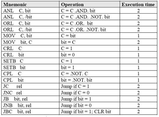
78 5.6 Boolean Instructions 5.7 Jump Instructions 72


79 5.8 Interfacing Keyboard to 85 Microcontroller The key board here we are interfacing is a matrix keyboard. This key board is designed with a particular rows and columns. These rows and columns are connected to the microcontroller through its ports of the micro controller 85. We normally use 8*8 matrix key board. So only two ports of 85 can be easily connected to the rows and columns of the key board. Whenever a key is pressed, a row and a column gets shorted through that pressed key and all the other keys are left open. When a key is pressed only a bit in the port goes high. Which indicates microcontroller that the key is pressed. By this high on the bit key in the corresponding column is identified. Once we are sure that one of key in the key board is pressed next our aim is to identify that key. To do this we firstly check for particular row and then we check the corresponding column the key board. To check the row of the pressed key in the keyboard, one of the row is made high by making one of bit in the output port of 85 high. This is done until the row is found out. Once we get the row next out job is to find out the column of the pressed key. The column is detected by contents in the input ports with the help of a counter. The content of the input port is rotated with carry until the carry bit is set. The contents of the counter is then compared and displayed in the display. This display is designed using a seven segment display and a BCD to seven segment decoder IC The BCD equivalent number of counter is sent through output part of 85 displays the number of pressed key. Fig 5. Interfacing Keyboard to 85 Microcontroller Fig 5.2 Circuit Diagram of Interfacing Keyboard to 85 73
80 5.9 Program for Keyboard Interfacing with 85 Start of main program: to check that whether any key is pressed start: mov a,#h mov p,a ;making all rows of port p zero mov a,#fh mov p,a ;making all rows of port p high press: mov a,p2 jz press ;check until any key is pressed after making sure that any key is pressed mov a,#h ;make one row high at a time mov r4,a mov r3,#h ;initiating counter next: mov a,r4 mov p,a ;making one row high at a time mov a,p2 ;taking input from port A jnz colscan ;after getting the row jump to check column mov a,r4 rl a ;rotate left to check next row mov r4,a mov a,r3 add a,#8h ;increment counter by 8 count mov r3,a sjmp next ;jump to check next row after identifying the row to check the colomn following steps are followed colscan:mov r5,#h in: rrc a ;rotate right with carry until get the carry jc out ;jump on getting carry inc r3 ;increment one count jmp in out: mov a,r3 74
81 da a ;decimal adjust the contents of counter before display mov p2,a jmp start ;repeat for check next key 5. Seven Segment Disply Interfacing with 85 Fig 5.3 Interfacing LEDS to 85 Microcontroller Fig 5.4 Seven Segment Display Fig 5.5 Connecting Seven segment Display with 85 75
. This is due to the following reasons: The declining prices of LCDs.")
82 5. LCD Interfacing This section describes the operation modes of LCDs, then describes how to program and interface an LCD to an 85 using Assembly and C. LCD operation: In recent years the LCD is finding widespread use replacing LEDs (seven-segment LEDs or other multisegment LEDs). This is due to the following reasons: The declining prices of LCDs. The ability to display numbers, characters, and graphics. This is in contrast to LEDs, which are limited to numbers and a few characters. Incorporation of a refreshing controller into the LCD, thereby relieving the CPU of the task of refreshing the LCD. In contrast, the LED must be refreshed by the CPU (or in some other way) to keep displaying the data. Ease of programming for characters and graphics. LCD pin descriptions The LCD discussed in this section has 4 pins. The function of each pin is given in Table 5-. Figure 5.6 shows the pin positions for various LCDs. Table 5. Function of Pins VCC> VSS> and VEE While Vcc and Vss provide +5V and ground, respectively, VEE is used for controlling LCD contrast. 76

83 RS, register select There are two very important registers inside the LCD. The RS pin is used for their selection as follows. If RS =, the instruction command code register is selected, allowing the user to send a command such as clear display, cursor at home, etc. If RS = the data register is selected, allowing the user to send data to be displayed on the LCD. R/W, read/write R/W input allows the user to write information to the LCD or read information from it. R/W = when reading; R/W = when writing. E, enable The enable pin is used by the LCD to latch information presented to its data pins. When data is supplied to data pins, a high-to-low pulse must be applied to this pin in order for the LCD to latch in the data present at the data pins. This pulse must be a minimum of 45 ns wide. DO-D7 The 8-bit data pins, DO - D7, are used to send information to the LCD or read the contents of the LCD's internal registers. To display letters and numbers, we send ASCII codes for the letters A - Z, a - z, and numbers - 9 to these pins while making RS =. Figure 5.6 Pin Positions. There are also instruction command codes that can be sent to the LCD to clear the display or force the cursor to the home position or blink the cursor. Table 2-2 lists the instruction command codes. We also use RS = to check the busy flag bit to see if the LCD is ready to receive information. The 77
84 busy flag is D7 and can be read when R/W = and RS =, as follows: if R/W=, RS =. When D7 = (busy flag = ), the LCD is busy taking care of internal operations and will not accept any new information. When D7 =, the LCD is ready to receive new information. Note: It is recommended to check the busy flag before writing any data to the LCD. Figure 5.7 Pin Positions for Various LCDs from Optrex Sending commands and data to LCDs with a time delay Program 5.: Communicating with LCD using a delay 78
85 To send any of the commands from Figure 5.6 to the LCD, make pin RS =. For data, make RS =. Then send a high-to-low pulse to the E pin to enable the internal latch of the LCD. This is shown in Program 5-. See Figure 5.7 for LCD connections. Program 5.2 Sending code or data to the LCD with checking busy flag The above code showed how to send commands to the LCD without checking the busy flag. Notice that we must put a long delay between issuing data or commands to the LCD. However, a much better way is to monitor the busy flag before issuing a command or data to the LCD. This is shown in Program 5.3. Program 5.3: Communicating with LCD using the busy flag 79
86 Figure 5.8. LCD Timing for Read ( L-to-H for E line) Notice in the above program that the busy flag is D7 of the command register. To read the command register we make R/W = and RS =, and a L-to-H pulse for the E pin will provide us the command register. After reading the command register, if bit D7 (the busy flag) is high, the LCD is busy and no information (command or data) should be issued to it. Only when D7 = can we send data or commands to the LCD. Notice in this method that no time delays are used since we are checking the busy flag before issuing commands or data to the LCD. Contrast the Read and Write timing for the LCD in Figures 5.8 and 5.9. Note that the E line is negative-edge triggered for the write while it is positive-edge triggered for the read. 8

87 Figure 5.9. LCD Timing for Write (H-to-L for E line) LCD data sheet In the LCD, one can put data at any location. The following shows address locations and how they are accessed. where AAAAAAA = to for line and AAAAAAA - to for line 2. See Table 2-3. Table 5.3 LCD Addressing The upper address range can go as high as for the 4-charac-ter-wide LCD, while for the 2-character-wide LCD it goes up to (9 decimal = binary). Notice that the upper range (binary) = 39 decimal, which corresponds to locations to 39 for the LCDs of 4x2 size. From the above discussion we can get the addresses of cursor positions for various sizes of LCDs. See Figure 2-5 for the cursor addresses for common types of LCDs. Note that all the addresses are in hex. Table 2-4 provides a detailed list of LCD commands and instructions. Table 2-2 is extracted from this table. 8

88 Figure 5. Cursor Addresses for Some LCDs 5.2 Stepper Motor Interfacing This section begins with an overview of the basic operation of stepper motors. Then we describe how to interface a stepper motor to the 85. Finally, we use Assembly language programs to demonstrate control of the angle and direction of stepper motor rotation. Stepper motors: A stepper motor is a widely used device that translates electrical pulses into mechanical movement. In applications such as disk drives, dot matrix printers, and robotics, the stepper motor is used for position control. Stepper motors commonly have a permanent magnet rotor (also called the shaft) surrounded by a stator. There are also steppers called variable reluctance stepper motors that do not have a PM rotor. The most common stepper motors have four stator windings that are paired with a center-tapped common as shown in Figure 5.. This type of stepper motor is commonly referred to as a. four-phase or unipolar stepper motor. The center tap allows a change of current direction in each of two coils when a winding is grounded, thereby resulting in a polarity change of the stator. Notice that while a conventional motor shaft runs freely, the stepper motor shaft moves in a fixed repeat-able increment, which allows one to move it to a precise position. This repeatable fixed movement is possible as a result of basic magnetic theory where poles of the same polarity repel and opposite poles attract. The direction of the rotation is dictated by the stator Poles. The stator poles are determined by the current sent through the wire coils. As the direction of the current is changed, the polarity is also changed causing the reverse motion of the rotor. The stepper motor discussed here has a total of 6 leads: 4 leads representing the four stator windings and 2 commons for the center-tapped leads. As the sequence of power is applied to each stator winding, the rotor will rotate. Table 5.4 Normal 4-Step Sequence 82

89 There are several widely used sequences where each has a different degree of precision. Table 5.4 shows a 2-phase, 4-step stepping sequence. It must be noted that although we can start with any of the sequences in Table 5.5, once we start we must continue in the proper order. For example, if we start with step 3 (), we must continue in the sequence of steps 4,,2, etc. Step angle Table 5.5 Stepper Motor Step Angle How much movement is associated with a single step? This depends on the internal construction of the motor, in particular the number of teeth on the stator and the rotor. The step angle is the minimum degree of rotation associated with a single step. Various motors have different step angles. Table 5.5 shows some step angles for various motors. In Table 5.5, notice the term steps per revolution. This is the total number of steps needed to rotate one complete rotation or 36 degrees (e.g., 8 steps x 2 degrees = 36). It must be noted that perhaps contrary to one's initial impression, a stepper motor does not need more terminal leads for the stator to achieve smaller steps. All the stepper motors discussed in this section have 4 leads for the stator winding and 2 COM wires for the center tap. Although some manufacturers set aside only one lead for the common signal instead of two, they always have 4 leads for the stators. Next we discuss some associated terminology in order to understand the stepper motor further. Example 5. Describe the 85 connection to the stepper motor of Figure 5. and code a program to rotate it continuously. Solution: The following steps show the 85 connection to the stepper motor and its programming. Use an ohmmeter to measure the resistance of the leads. This should identify which COM leads are connected to which winding leads. The common wire(s) are connected to the positive side of the motor's power supply. In many motors, +5 V is sufficient. The four leads of the stator winding are controlled by four bits of the 85 port (Pl.O - P.3). However, since the 85 lacks sufficient current to drive the stepper motor windings, we must use a driver such as the ULN23 to energize the stator. Instead of the ULN23, we could have used transistors as drivers, as shown in Figure 7-9. However, notice that if transistors are used as drivers, we must also use diodes to take care of inductive current generated when the coil is turned off. One reason that using the ULN23 is preferable to the use of transistors as drivers is that the ULN23 has an internal diode to take care of back EMF. 83
90 Change the value of DELAY to set the speed of rotation. We can use the single-bit instructions SETB and CLR instead of RR A to create the sequences. Figure Connection to Stepper Motor Steps per second and rpm relation: The relation between rpm (revolutions per minute), steps per revolution, and steps per second is as follows. The four-step sequence and number of teeth on rotor The switching sequence shown earlier in Table 5.4 is called the 4-step switching sequence since after four steps the same two windings will be "ON" How much movement is associated with these four 84
91 steps? After completing every four steps, the rotor moves only one tooth pitch. Therefore, in a stepper motor with 2 steps per revolution, the rotor has 5 teeth since 4x5 = 2 steps are needed to complete one revolution. This leads to the conclusion that the minimum step angle is always a function of the number of teeth on the rotor. In other words, the smaller the step angle, the more teeth the rotor passes. 5.3 Servo Motor Servos are DC motors with built in gearing and feedback control loop circuitry. And no motor drivers required. They are extremely popular with robot, RC plane, and RC boat builders. Most servo motors can rotate about 9 to 8 degrees. Some rotate through a full 36 degrees or more. However, servos are unable to continually rotate, meaning they can't be used for driving wheels, unless they are modified (how to modify), but their precision positioning makes them ideal for robot legs and arms, rack and pinion steering, and sensor scanners to name a few. Since servos are fully self-contained, the velocity and angle control loops are very easy to implement, while prices remain very affordable. To use a servo, simply connect the black wire to ground, the red to a 4.8-6V source, and the yellow/white wire to a signal generator (such as from your microcontroller). Vary the square wave pulse width from -2 ms and your servo is now position/velocity controlled. Pulse width modulation (PWM) is a powerful technique for controlling analog circuits with a processor's digital outputs. PWM is employed in a wide variety of applications, ranging from measurement and communications to power control and conversion. The general concept is to simply send an ordinary logic square wave to your servo at a specific wave length, and your servo goes to a particular angle (or velocity if your servo is modified). The wavelength directly maps to servo angle. Fig 5.9 Pulse for controlling Servo motor 5.3. Controlling the Servo Motor PWM Pulse width modulation (PWM) is a powerful technique for controlling analog circuits with a processor's digital outputs. PWM is employed in a wide variety of applications, ranging from measurement and communications to power control and conversion. The general concept is to simply send an ordinary logic square wave to your servo at a specific wave length, and your servo goes to a particular angle (or velocity if your servo is modified). The wavelength directly maps to servo angle. Programmable Counter Array (PCA) The PCA is a special modules in Philips P89V5RD2 which includes a special 6-bit Timer that 85
92 has five 6-bit capture/compare modules associated with it. Each of the modules can be programmed to operate in one of four modes: rising and/or falling edge capture, software timer, high-speed output, or pulse width modulator. Each module has a pin associated with it in port. Module is connected to P.3 (CEX), module to P.4 (CEX), etc. Registers CH and CL contain current value of the free running up counting 6-bit PCA timer. The PCA timer is a common time base for all five modules and can be programmed to run at: /6 the oscillator frequency, /2 the oscillator frequency, the Timer overflow, or the input on the ECI pin (P.2). The timer count source is determined from the CPS and CPS bits in the CMOD SFR. In the CMOD SFR there are three additional bits associated with the PCA. They are CIDL which allows the PCA to stop during idle mode, WDTE which enables or disables the Watchdog function on module 4, and ECF which when set causes an interrupt and the PCA overflow flag CF (in the CCON SFR) to be set when the PCA timer overflows. The Watchdog timer function is implemented in module 4 of PCA. Here, we are interested only PWM mode. 85 Pulse width modulator mode All of the PCA modules can be used as PWM outputs. Output frequency depends on the source for the PCA timer. All of the modules will have the same frequency of output because they all share one and only PCA timer. The duty cycle of each module is independently variable using the module's capture register CCAPnL. When the value of the PCA CL SFR is less than the value in the module's CCAPnL SFR the output will be low, when it is equal to or greater than the output will be high. When CL overflows from FF to, CCAPnL is reloaded with the value in CCAPnH. This allows updating the PWM without glitches. The PWM and ECOM bits in the module's CCAPMn register must be set to enable the PWM mode. For more details see P89V5RD2 datasheet. This is an example how to control servos with 85 by using PWM. The schematic is shown below. I use P.4 (CEX) to control the left servo and P.2 (CEX2) to control the right servo. Here, I use GWS servo motor model S3T STD. I need three states of duty cycle: 2 ms to Stop the servo ms to Rotate Clockwise Calculation for duty cycle (for XTAL MHz with 6 Clock/Machine cycle) Initial PWM Period = 2mS (8.432MHz /6-Cycle Mode) Initial PCA Count From Timer Overflow Cycle of Timer = (/8.432MHz)x6 =.326 us Timer AutoReload = 24 Cycle = us Cycle PCA = [(/8.432MHz)x6]x24 = us Period 2mS of PCA = 2ms/78.25us = 256 (CL Reload) CL (2mS) = 256 Cycle Auto Reload Load CCAPxH (.ms) = = 243 (243,244,...,255 = 3 Cycle) Load CCAPxH (2.mS) = = 23 (23,23,...,255 = 26 Cycle) 86
 Compiler : SDCC /* Control the Left servo */ void ServoL_back() { CCAPH = 243; } void ServoL_forward() { CCAPH = 23; } void ServoL_stop() { CCAPH = ; } /* Control the Right")
93 Fig 5. Schematic Control Program Filename : pwm_servos.h Hardware : Controller -> P89V5RD2 XTAL -> MHz Mode -> 6 Clock/MC I/O : P.4 -> Left (PWM-CEX) P.5 -> Right (PWM-CEX2) Compiler : SDCC /* Control the Left servo */ void ServoL_back() { CCAPH = 243; } void ServoL_forward() { CCAPH = 23; } void ServoL_stop() { CCAPH = ; } /* Control the Right servo */ void ServoR_back() { CCAP2H = 23; } void ServoR_forward() { 87
94 CCAP2H = 243; } void ServoR_stop() { CCAP2H = ; } /* Initialize the PCA and PWM mode */ void Servos_init() { /* Initial Timer Generate Overflow PCA */ TMOD = x2; /* Timer Mode2 : 8bit auto reload */ TH = 6; /* , 8.25usec Auto-relead (2msec/PWM) */ TL = TH; TCON = x; /* setb TR, TCON or,*/ /*Initial PWM Period = 2mS (8.432MHz /6-Cycle Mode) Initial PCA Count From Timer Overflow Cycle of Timer = (/8.432MHz)x6 =.326uS Timer AutoReload = 24 Cycle = 78.25uS Cycle PCA = [(/8.432MHz)x6]x24 = 78.25uS Period 2mS of PCA = 2ms/78.25us = 256(CL Reload) CL(2mS) = 256 Cycle Auto Reload Load CCAPxH(.mS) = = 243 (243,244,...,255 = 3 Cycle) Load CCAPxH(2.mS) = = 23 (23,23,...,255 = 26 Cycle)*/ CMOD=x4; CCAPM=x42; CCAPM2=x42; CCAPH=x; CCAP2H=x; CCON=x4; } test.c #include <p89v5rd2.h> #include "pwm_servos.h" void PowerOn() { unsigned char inner, outer; IE = x; P = xff; /* Motor STOP */ for (outer = x; outer < x; outer++) { /* Delay for a while */ for (inner = x; inner < xff; inner++); } Servos_init(); IE = x8; /* Start interrupt */ } void main() { PowerOn(); ServoR_forward(); ServoL_back(); while (); } 5.4 Washing Machine Control Many washing m/c shell in the market has mechanical controlled sequence for activated the timer and the sequence back and forth for their motor; washing motor or spinning motor. Spinning motor control only has one direction only, and its simple could be changed to the discrete mechanical timer which sell on the market. But washing motor control has 2 direction for this purpose, it means to squeeze the clothes, it must go to forward and then reversed. The sequence is like this: First, go to forward direction for about a few seconds Than stop, while the chamber is still rotate 88
95 Second, go back to reverse direction for about a few seconds Than stop, while the chamber is still rotate And so on, back and forth, until the the timer elapsed 5.4. Schematic Timing sequence like the above description, can be implemented with many way, by using discrete electronic components, timer, using a program or a microcontroller or microprocessor, etc. Because I am learning the PIC microcontroller for right now, I will implement this function using this microcontroller, but for you who familiar with another kind of microcontroller my adapted it to your purpose. By using PIC micro, it can be made more compact. First I plan to make 2 buttons, for set the timer and another for reset the timer or for the emergency stop push button. Then to know the timer works or not, I need a visual display. For this purpose I will use 7-segmen display showing the rest of the timer. To run the motor sequence of course I need a pair of relays (power relays, about 3 Amperes output), one for forward and another for reverse option. I will use the very common family of PIC micro, ie : 6F84A, because this is the most popular type and very simples used and very much used. Also can be obtained easily in the market. But this is the medium type of PIC micro family. It has kbyte of memory (EEPROM type) and 3 I/O pins. It can be reprogrammable thousands times. Because the I/O just only 3 pins, I used a BCD to 7-segmen chip. So it will left a few I/O pins for expanded in the future. You can omitted this chip for timing sequence purpose and save one IC price, because the I/O just exactly enough. I/O port A- = SET push button I/O port A- = RST push button I/O port A-2 = Reserved I/O port A-3 = Reserved I/O port A-4 = Reserved I/O port B- = Forward Relay (Run motor forward) I/O port B- = Reverse Relay (Run motor reverse) I/O port B-2 = Activated unit 7-segmen (multiplexed) I/O port B-3 = Activated ten 7-segmen (multiplexed) I/O port B-4 = BCD data A (for 7-segmen) I/O port B-5 = BCD data B (for 7-segmen) I/O port B-6 = BCD data C (for 7-segmen) I/O port B-7 = BCD data D (for 7-segmen) Also integrated power supply to run it modularly The I/O can be configured as input pin or output pin bit-ly. It is up to you to choose the I/O pin number goes to what function, but it infect the program firmware of course. Once you choose, then it is just like that, except you also change both, the program and the hardware Working of Washing Machine The direction of rotation can be controlled when switchs is in position A, coil L of the motor receives the current directly, whereas coil L2 receives the current with a phase shift due to capacitor C. So the rotor rotates in clockwise direction (see Fig. 2(a)). When switch S is in position B, the reverse happens and the rotor rotates in anti-clock wise direction Thus switch S can change the rotation direction. The motor cannot be reversed instantly. It needs a brief pause between switching directions, or else it may get damaged. For this purpose, another spin direction control timer (IC2) is employed. It is realised with an IC 555. This timer gives an alternate on and off time duration of seconds and 3 seconds, respectively. So after every l seconds of running (either in clockwise or anti clockwise direction), the motor stops for a brief duration of 3 seconds. The values 89
96 of R3 and R4 are calculated accordingly. The master timer is realised with monostable IC555 (IC) and its on time is decided by the resistance of -mega- ohm potmeter VR. A 47-kilo-ohm resistor is added in series so that even when the VR knob is in zero resistance position, the net series resistance is not zero Fig 5. Circuit Diagram of Washing Machine Fig 5.2 Rotation of Motor 9
97 QUESTION BANK 9
98 UNIT- 885 & 886 PROCESSOR Two Marks Questions with Answers. What is microprocessor? Give the power supply &clock frequency of 885 A microprocessor is a multipurpose, programmable logic device that reads binary instructions from a storage device called memory accepts binary data. As input and processes data according to those instructions and provides result as output. The power of 885 is +5v and clock frequency in 3MHZ. 2. List few applications of microprocessor-based system. It is used: For measurements, display and control of current, voltage, Temperature, pressure, etc. For traffic control and industrial tool control. For speed control of machines. 3. What are the functions of an accumulator? The accumulator is the register associated with the ALU operations and sometimes I/O operations. It is an integral part of ALU. It holds one of d a t a t o be processed by ALU. It also temporarily stores the result of the operation performed by the ALU. 4. List the 6 bit registers of 885 microprocessor. Stack pointer (sp) and program counter (pc). 5.List the allowed register pairs of 885. B-C register pair D-C register pair H-L register pair. 6.Mention the purpose of SID and SOD lines SID(serial input data line): It is an input line through which the microprocessor accepts serial data. SOD(serial output data line): 7.What is an opcode? It is an output line through which the microprocessor sends output serial data. The part of the instruction that specifies the operation to be performed is called the operation code or opcode. 92
99 8. What is the function of IO/M signal in the 885? It is a statussignal. It is used to differentiate between memory locations and I/O operations w h e n this signal is low (IO/M=) it denotes the memory related operations. When this signal is high (IO/M=) it denotes an I/O operation 9. What is an operand? The data on which the operation is to be performed is called as an operand.. How many address lines in a 496*8 EPROM CHIP? 2 Address lines.. Control signals used for DMA operation are HOLD HLDA 2. What is meant by wait state? This state is used by slow peripheral devices. The peripheral devices can transfer the data to or from the microprocessor by using READY input line. The microprocessor remains in the wait state as long as READY line is low. During the wait state, the contents of the address, address/data and control buses are held constant. 3. What is meant by polling? Polling or device polling is a process which identifies the device that has interrupted the microprocessor. 4. What is meant by interrupt? Interrupt is an external signal that causes a microprocessor to jump to a specific subroutine. 5. Explain priority interrupts of 885? The 885 microprocessor has five interrupt inputs. They are TRAP, RST7.5, RST 6.5, RST 5.5, and INTR. these interrupts have a fixed priority of interrupt service. If two or more interrupts go high at the same time, the 885 will service them on priority basis. The TRAP has the highest priority followed by RST7.5, RST6.5, and RST5.5. The p r i o r i t y of interrupts in 885 is shown in the table. 6. What is a microcomputer? Interrupts TRAP RST7.5 2 RST6.5 3 RST5.5 4 INTR 5 priority A computer that is designed using a microprocessor as its CPU is called microcomputer. 93
100 7. What is the signal classification of 885? All the signals of 885 can be classified into 6 groups Address bus Data bus Control and status signals Power supply and frequency signals Externally intiated signals Serial I/O ports 8. What are operations performed on data in 885? The various operations performed are Store 8-bit data Perform arithmetic and logical operations Test for conditions Sequence the execution of instructions Store data temporarily during execution in the defined R/W Memory locations called the stack 9. Steps involved to fetch a byte in 885? The pc places the 6-bit memory address on the address bus The control unit sends the control signal RD to enable the memory chip The byte from the memory location is placed on the data bus The byte is placed in the instruction decoder of the microprocessor and the task is carried out according to the instruction. 2. How many interrupts does 885 have mention them The 885 has 5 interrupt signals they have INTR, RST7.5, RST6.5, RST5.5 and TRAP 2. Basic concepts in the memory interfacing? The primary function of memory interfacing is that the microprocessor should be able to read from and write into a given register of a memory chip.to perform these operations the microprocessor should, Be able to select the chip Identify the register Enable the appropriate buffer 22. Define instruction cycle, machine cycle and T-state? Instruction cycle is defined as the time required completing the execution of an instruction. Machine cycle is defined as the time required completing one operation of accessing memory, I/O or acknowledging an external request. T cycle is defined as one subdivision of the operation performed in one clock period. 23. What is the use of ALE? The ALE is used to latch the lower order address so that it can be available in T2 and T3 and used for identifying the memory address. During T the ALE goes high, the latch is transparent ie, 94
101 the output changes according to the input data, so the output of the latch is the lower order address. When ALE goes low, the lower order address is latched until the next ALE. 24. How many machine cycles does 885 have? Mention them. The 885 have seven machine cycles they are Opcode fetch Memory read Memory write I/O read I/Owrite Interrupt acknowledge Bus idle 25. Explain the signals HOLD, READY and SID. HOLD indicates that a peripheral such a DMA controller is requesting the use of address bus, data bus and control bus. READY is used to delay the microprocessor read or write cycles until a slow responding peripheral is ready to accept or send data. SID is used to accept serial data bit by bit. 26. What is the use of bidirectional buffer? It is used to increase the driving capacity of data bus. The data bus of the microcomputer system is bidirectional, so it requires a buffer that allow the data to flow in both directions. 27. Give the register organization of 885? W(8)Register Z(8) Register B(8)Register E(8)Register H(8)Register L(8) Register Stack pointer(6) Program counter(6) 28. What is the microcontroller and microcomputer? Microcontroller is a device that includes microprocessor, memory and I/O signal lines on a single chip, fabricated using VLSI technology. Microcomputer is a computer that is designed using microprocessor as its CPU.it includes microprocessor, memory and I/O. 29. Define flags? The flags are used to reflect the data conditions in the accumulator. The 885 flags are S-sign flag Zero flag Auxiliary flag Parity flag Carry Flag 95
102 3. Difference between memory mapped I/O and peripheral I/O? MEMORY MAPPEED I/O 6-bit device address The data transfer between any generalpurpose register and I/O port The memory map(64kb)is shared between I/O device and system memory More hardware is required to decode 6-bit address 8-bit device address PERIPHERAL I/O The data transfer only between accumulator and I/O port The I/O map is independent of the memory map,256 input device and 256 output device Less hardware is required to decode 8-bit address 3. What is interfacing? An interface is a shared boundary between the devices which involves sharing information. Interfacing is the process of making two different systems communicate with each other. 32. What is memory mapping? The assignment of memory address to various registers in a memory chip is called as memory mapping. 32. What is I/O mapping? The assignment of address to various I/O devices in the memory chip is called as I/O Mapping.. Describe the functional pin diagram of Describe the functional block diagram of Explain the 885 interrupt system in detail. 8 Marks Questions 4. Explain various machine cycles supported by What is the difference between minimum and maximum modes of 886? How are T modes selected? 6. Describe the sequence of event that may occur during the different T state in the opcode fetch machine cycle of List out the maskable and non maskable interrupts available in Write short notes on addressing memory 9. Give the functions of NMI, BHE and TEST pins of 886. Write notes on addressing input and output devices.. Describe the sequence of event that may occur during the different T state in the opcode fetch machine cycle of Explain the concept of pipelining in 886. Discuss its advantages and disadvantages. 96
103 6 Marks Questions. Draw and explain the architecture of Design a microprocessor system to interface an 8K 8 EPROM and 8K 8 RAM. 3. How many interrupts are available in 886? List the predefined software interrupts available in Explain the minimum mode of operation of Explain the Maximum mode of operation of Draw and explain the architecture of
104 UNIT-2 PROGRAMMING OF 885 PROCESSOR Two Marks Questions with Answers. What is an instruction? An instruction is a binary pattern entered through an input device to command the microprocessor to perform that specific function. 2. How many operations are there in the instruction set of 885 microprocessor? There are 74 operations in the 885 microprocessor 3. List out the five categories of the 885 instructions. Give e.g. of the instructions for each group? Data transfer group MOV,MVI,LXI Arithmetic group ADD,SUB,INR. Logical group- ANA,XRA,CMP. Branch group JMP,JNZ,CALL. Stack I/O and machine control group PUSH,POP,IN,HLT. 4. Explain the difference between a JMP instruction and CALL instruction. A JMP instruction permanently changes the program counter. A CALL instruction leaves information on the stack so that the original program execution sequence can be resumed. 5. Explain the purpose of the I/O instructions IN and OUT The IN instruction is used to move data from an I/O port in to the accumulator. The OUT instruction is used to move data from the accumulator to an I/O port. The IN and OUT instructions are used only on microprocessor, which use address space for interfacing. a separate 6. What is the difference between the shift and rotate instructions? A rotate instruction is a closed loop instruction.that is the data moved out at one end is put back in at the other end. The shift instruction loses the data that is moved out of the last bit locations. 7. List the four instructions which control the interrupt structure of the 885 microprocessor? DI(disable interrupts) EI(enable interrupts) RIM(read interrupt masks) SIM(set interrupt masks) 8. Mention the categories of instruction and give two ex for each category? The instructions of 885 can be categorized in to the following five 98
105 . Data transfer MOV RD,RS,STA 6-BIT 2. Arithmetic ADD R,DCR M. 3. Logical XRI 8- bit,rar 4. Branching JNZ CALL 6-bit 5. Machine control HLT,NOP 9. Explain LDA, STA AND DAA instructions LDA copies the data byte in to the accumulator from the memory location specified by the 6-bit address. STA copies the data byte from the accumulator in the memory location specified by 6-bit address. DAA changes the content of the accumulator from binary to 4-bit BCD digits. Explain the different instruction formats with ex? The instruction set is grouped in to the following formats One byte instruction Two byte instruction MVI A,39H Three byte instruction JMP 2345H MOV C,A. What is the use of addressing modes, mention the different types? The v arious formats of specifying the operands are called as addressing modes, it is used to access the operands or data. The different types are as follows. Immediate addressing 2. Register addressing 3. Direct addressing 4. Indirect addressing 5. Implicit addressing 2. Define stack and stack related instructions? The stack is a group of memory locations in the R/W memory that is used for the temporary storage of binary information during the execution of the program. The stack related instructions are PUSH and POP 3. Why do we use XRA A instruction? The XRA A instruction is used to value H clear the contents of the accumulator and store the 4. Compare CALL and PUSH instructions CALL When CALL is executed the microprocessor automatically stores the 6-bit address of the instruction next to CALL on the stack When CALL is executed the stack pointer is decremented by two PUSH The program uses the instruction PUSH to save the contents of the register pair on the stack When PUSH is executed the stack pointer register is decremented by two 5. How does the microprocessor differentiate b/w data and instruction? When the first m/c code of an instruction is fetched and decoded in the instruction register, the 99
106 microprocessor recognizes the n u m b e r o f b y t e s r e q u i r e d to f e t c h t h e e n t i r e instruction. For ex MVI A,data, the second byte is always considered as data. If the data byte is omitted by mistake whatever is in that memory location will be considered as data and the byte after the data will be treated as the next instruction. 6. Compare RET and POP RET RET transfers the content of the top two locations of the stack to the PC When RET is executed the SP is incremented by two. And it has 8 conditional RETURN instructions POP Pop transfers the content of the top two locations of the stack to the specified register pair When POP is executed the SP is incremented by two and no conditional POP instructions 7. What are subroutine? Procedures are group of instructions stored as a separate program in memory and it is called from the main program in memory and it is called from the main program whenever required. The type of procedure depends on where the procedures are stored in memory. If it is in the same code segment as that of the main program then it is a near procedure otherwise it is a far procedure. 8. What is a recursive procedures? A recursive procedure is a procedure, which calls itself. Recursive procedures are used to work with complex data structures called trees. If the procedure is called with N=3, then the N is decremented by after each procedure CALL and the procedure is called until N=. 9. How to access subroutine with in the main program procedure? accessed by CALL & RET instruction machine code of instruction is put only once in the memory iii)with procedures less memory is required parameters can be passed in registers, memory location or stack 2. Define stack? Stack is a sequence of RAM memory locations defined by the programmer. 2. How the microprocessor is synchronized with peripherals? The timing and control unit synchronizes all the microprocessor operations with clock and generates control signals necessary for communication between the microprocessor and peripherals. 22. What is the minimum s/m and how it is formed in 885? A minimum s/m is one which is formed using minimum number of IC chips. The 885 based minimum s/m is formed using 855, 8355 &
107 8 Marks Questions. Write a program to arrange /n numbers in ascending order. 2. Write a program to unpack a two digit BCD number stored at memory location CH 3. Write a program to calculate the factorial of a number between to 8 4. Write a program to find the number of negative, zero and positive numbers 5. Write a program to ADD two 8 Bit numbers. 6. Explain the stack operations with an example 7. Describe an Input/Output instructions with an example. 8. Explain the BCD to Decimal code conversion technique and write 885 assembly language program for the same 9. Explain the BCD to Seven Segment code conversion technique and write 885 assembly language program for the same.. Discuss in detail about jump instructions. Discuss the operation of Looping, Counting and indexing with Look up table. 6 Marks Questions. Explain the addressing modes of 885 with example 2. Explain the Different types of instruction in Explain the Arithmetic and logical instruction in 885 with example 4. With an example, Explain the operation of Data transfer instructions 5. Discuss in detail about the operation of Subroutines instructions.
108 UNIT- 3 PERIPHERAL INTERFACING Two Marks Questions with Answers. What is the use of 85 chip? Intel s 825A is a universal synchronous asynchronous receiver and transmitter compatible with Intel s Processors. This may be programmed to operate in any of the serial communication modes built into it. This chip converts the parallel data into a serial stream of bits suitable for serial transmission. It is also able to receive a serial stream of bits and converts it into parallel data bytes to be read by a microprocessor. 2. What are the different types of methods used for data transmission? The data transmission between points involves unidirectional or bi-directional transmission of meaningful digital data through a medium. There are basically there modes of data transmission Simplex Duplex Half Duplex In simplex mode, data is transmitted only in one direction over a single communication channel. For example, a computer (CPU) may transmit data for a CRT display unit in this mode. In duplex mode, data may be transferred between two trans receivers in both directions simultaneously. In half duplex mode, on the other hand, data transmission may take place in either direction, but at a time may be transmitted only in one direction. For example, a computer may communication with a terminal in this mode. When the terminal sends data (i.e. terminal is sender).the message is received by the computer (i.e. computer is receiver). However, it is not possible to transmit data from the computer to terminal and from terminal to the computer simultaneously. 3. What is the various programmed data transfer method? Synchronous data transfer Asynchronous data transfer Interrupt driven data transfer 4. What is synchronous data transfer? It is a data method which is used when the I/O device and the microprocessor match in speed. The transfer a data to or from the device, the user program issues a suitable instruction addressing the device. The data transfer is completed at the end of the execution of this instruction. 5. What is asynchronous data transfer? It is a data transfer method which is used when the speed of I/O device does not match with the speed of the microprocessor. Asynchronous data transfer is also called as Handshaking. 2
109 6. What are the functional types used in control words of 825a? The control words of 825A are divided into two functional types Mode Instruction control word: - This defines the general operational characteristics of 825A. Command Instruction control word: - The command instruction controls the actual operations of the selected format like enable transmit/receiver, error reset and modem control. 7. What are the basic modes of operation of 8255? There are two basic modes of operation of 8255, viz. I/O mode. BSR mode In I/O mode, the 8255 ports work as programmable I/O ports, while in BSR mode only port C (PC-PC7) can be used to set or reset its individual port bits. Under the IO mode of operation, further there are three modes of operation of 8255, So as to support different types of applications, viz. mode, mode, and mode 2. Mode - Basic I/O mode Mode -Strobe I/O mode Mode 2- Strobe bi-direction I/O 8. Write the features of mode in 8255? Two 8-bit ports (port A and port B) and two 4-bit ports (port C upper and lower) are available. Thetwo 4-bit ports can be combined used as a third8-bitport. Any port can be used as an input or output port. Output ports are latched. Input ports are not latched. A maximum of four ports are available so that overall 6 I/O configurations are possible. 9. What are the features used mode in 8255? Two groups A and group B are available for strobe data transfer. Each group contains one 8-bit data I/O port and one 4-bit control/data port. The 8-bit data port can be either used as input or output port. The inputs and outputs both are latched. Out of 8-bit port C, PC-PC2 is used to generate control signals for port B and PC3=PC5 are used to generate control signals for port A. The inputs PC6, PC7 may be used as independent data lines.. What are the signals used in input control signal and output control signals? Input control signals STB (Strobe input) Output control signal OBF (Output buffer full) INTR (Interrupt request) IBF (Input buffer full) INTR (Interrupt request) ACK (Acknowledge input). What are the features used mode 2 in8255? The signals 8-bit port in group A is available. 3
110 The 8-bit port is bi-directional and additionally a 5-bit control port is available. Three I/O lines are available at port C, viz PC2-PC. Inputs and output are both latched. The 5-bit control port C (PC3-PC7) is used for generating/accepting handshake Signals for the 8-bit data transfer on port A. 2. What are the modes of operation used in 8253? Each of the three counters of 8253 can be operated in one of the following six modes of operation. Mode (Interrupt on terminal count) Mode (Programmable monoshot) Mode 2 (Rate generator) Mode 3 (Square wave generator) Mode 4 (Software triggered strobe) Mode 5 (Hardware triggered strobe) 3. What are the different types of write operations used in 8253? There are two types write operation in 8253 Writing a control word register Writing a count value into a count register The control word register accepts data from the data buffer and initialize Initializing the operating modes (mode - mode 4) Selection of counters (counter - counter 2) Choose binary /BCD counters. Loading of the counter registers. The mode control register is a write only register and the CPU cannot read its contents. 4. Give the different types of command words used in 8259A The command words of 8259A are classified in two groups Initialization command words (ICWs) Operation command words (OCWs) 5. Give the operation modes of 8259A? Fully Nest Mode End of Interrupt Automatic Rotation Automatic EOI mode Specific Rotation Special Mask Mode Edge and level Triggered Mode Reading 8259 Status Poll command Special Fully Nested Mode 4
111 Buffered Mode Cascade Mode 6. Define scan counter? The scan counter has two modes to scan the key matrix and refresh the display. In the encoded mode, the counter provides binary count that is to be externally decoded to provide the scan lines for keyboard and display. In the decoded scan mode, the counter internally decodes the least significant 2 bit and provides a decoded out of 4 scan on SL3-SL 3. The keyboard and display both are in the same mode at a time. 7. What is the output modes used in 8279? 8279 provides two output modes for selecting the display options. Display scan In this mode, 8279 provides 8 or 6 character- multiplexed displays those can be organized as dual 4-bit or single 8-bit display units. Display Entry 8279 allows options for data entry on the displays. The display data is entered for display from the right side or from the left side. 8. What are the modes used in keyboard modes? Scanned Keyboard mode with 2 Key Lockout Scanned K e y b o a r d w i t h N -Key Rollover. Scanned Keyboard Special Error Mode. Scanned Matrix Mode. 9. What are the modes used in display modes?. Left Entry Mode In the left entry mode, the data is entered from the left side of the display unit. 2. Right Entry Mode In the right entry mode, the first entry to be displayed is entered on the rightmost display. 2. What is the use of modem control unit in 825? The modem control unit handles the modem handshake signals to coordinate the communication between the modem and the USART. 2. List the operation modes of 8255? a) I/O Mode Mode - Simple Input/Output. Mode - Strobe Input/Output (handshake mode) Mode 2- Strobe bi-directional mode b) Bit Set/Reset Mode. 22. What is a control word? It is a word stored in a register (control register) used to control the operation of a program digital device. 5
112 23. What is the purpose of control word written to control register in 8255? The control words written to control register specify an I/O function for each I/O port. The bit D7 of the control word determines either the I/O functions of the BSR function. 24. What is the size of ports in 8255? Port - A : 8- bits Port - B : 8- bits Port -CU : 4- bits Port -CL : 4- bits 25. What is an USART? USART stands for universal Synchronous / Asynchronous Receiver / Transmitter. It is a programmable communication interface that can communicate by using either synchronous or asynchronous serial data. 26. What is the use of 825 chip? 825 chip is mainly used as the asynchronous serial interface between the processor and the external equipment. 27. The 8279 is a programmable interface. Keyboard/ Display 28. List the major components of the Keyboard/ Display interface. Keyboard section Scan section Display section CPUinterface section 29. What is Key bouncing? Mechanical switch are used as keys in most of the keyboard. When a key is pressed the contact bounce back and forth and settle down only after a small time delay (about 2ms). Even though a key is actuated once, it will appear to have been actuated several times. This problem is called Key Bouncing 3. What is TXD? TXD- Transmitter Data Output This output pin carries serial of the transmitted data bits along with other information like start bit, stop bits and priority bit. 3. Define HRQ? The hold request output request the access of the system bus. In non- cascaded 8257 systems, this is connected with HOLD pin of CPU. In cascade mode, this pin of a slave is connected with a DRQ input line of the master 8257, while that of the master is connected with HOLD input of the CPU. 6
113 32. What is RXD? RXD- Receive Data Input This input pin of 825A receives a composite stream of the data to be received by 825A. 33. What are the internal devices of a typical DAC? The internal devices of a DAC are R/2R resistive network, an internal latch and current to voltage converting amplifier. 34. What is setting or conversion time in DAC? The time taken by the DAC to convert a given digital data to corresponding analog signal is called conversion time. 35. What are the different types of ADC? The different types of ADC are successive approximation ADC, counter type ADC, flash type ADC, integrator converters and voltage to frequency converters. 8 Marks Questions. Using model, write a program to communicate between two microprocessors using Bring about the features of Explain the advantages of using the USART chips in microprocessor based systems 4. Show the control word format of 8255 and explain how each bit is programmed 5. Use RST 5.5 instead of RST 7.5 and change mask pattern accordingly 6. Describe with any one of the mode configurations of 8254 timer in detail 7. Use RST 5.5 instead of RST 7.5 and change mask pattern accordingly 8. Bring about the features of With neat block diagram explain the functions of Explain the advantages of using the keyboard and display controller chips in microprocessor based system. 7
114 6 Marks Questions. Explain any one of the modes of 8255 in detail 2. With neat block diagram explain PPI 3. Explain the working of 8254 timer 4. Explain how to convert an analog signal into digital signal 5. Explain the 7 segment LED interface with microprocessor. 8
115 UNIT-IV MICROCONTROLLERS 85 Two Marks Questions with Answers. What is mean by microcontroller? A device which contains the microprocessor with integrated peripherals like memory, serial ports, parallel ports, timer/counter, interrupt controller, data acquisition interfaces like ADC, DAC is called microcontroller. 2. Explain DJNZ instruction of Intel 85 microcontroller? DJNZ Rn, rel Decrement the content of the register Rn and jump if not zero. DJNZ direct, rel Decrement the content of direct 8- bit address and jump if not zero. 3. State the function of RS and RS bits in the flag register of Intel 85 microcontroller? RS, RS- Register bank select bits RS, RS- Bank Bank Bank Bank 2 Bank 3 4. Give the alternate functions for the port pins of port3? RD WR T T INT INT TXD RXD RD Read data control output WR Write data control output T Timer / counter external input or test pin T Timer / counter external input or test pin INT Interrupt input pin INT interrupt input pin TXD Transmit data pin for serial port in UART mode RXD Receive data pin for serial port in UART mode 5. Specify the single instruction, which clears the most significant bit of B register of 85, without affecting the remaining bits. Single instruction, which clears the most significant bit of B register of 85, without affecting the remaining bits, is CLR B Explain the function of the pins PSEN and EA of 85. PSEN: PSEN stands for program store enable. In 85 based system in which an external 9
116 ROM holds the program code, this pin is connected to the OE pin of the ROM. EA: EA stands for external access. When the EA pin is connected to Vcc, program fetched to address H through FFFH are directed to the internal ROM and program fetches to addresses H through FFFFH are directed to external ROM/EPROM. When the EA pin is grounded, all addresses fetched by program are directed to the external ROM/EPROM. 7. Explain the 6-bit registers DPTR and SP of 85. DPTR: DPTR stands for data pointer. DPTR consists of a high byte (DPH) and a low byte (DPL). Its function is to hold a 6-bit address. It may be manipulated as a 6- bit data registers. It serves as a base register in indirect jumps, lookup table instructions and external data transfer. SP: SP stands for stack pointer. SP is a 8-bit wide register. It is incremented before data is stored during PUSH and CALL instructions. The stack array can reside anywhere in-chip RAM. The stack pointer is initiailsed to 7H after a reset. This causes the stack to begin at location. 8H. 8. Name the special functions registers available in 85. Accumulator B Register Stack pointer. Data pointer Interrupt priority control register. Interrupt enable control register. 9. Explain the register IE format of 85. EA ET2 ES ET EX ET EX EA- Enable all control bit. ET2- Timer 2 interrupt enable bit. ES- Enable serial port control bit. ET- Enable Timer control bit. EX-Enable external interrupt control bit. ET-Enable Timer control bit. EX-Enable external interrupt control bit.. Compare Microprocessor and Microcontroller. Microprocessor Microcontroller. Microprocessor contains ALU, general Microcontroller contains the circuitry of Purpose register counter, clock timing microprocessor and in addition it has Circuit and interrupt circuit. Built-in ROM, RAM, I/O devices and counter. 2. It has many instructions to move data It has many instructions to move between memory and CPU. data between memory and CPU. 3. It has one or two bit handling it has many bit handling instructions. instruction.
117 4. Access times for memory and I/O Less access times for built-in memory Devices are more. and I/O devices. 5. Microprocessor based system Microcontroller based system requires requires more hardware less hardware reducing PCB size and Increasing the reliability.. Name the five interrupt sources of 85? The interrupt are: Vector address External interrupt : IE: 3H Timers interrupt : TF: BH External interrupt : IE: 3H Timers interrupt : TF:BH Serial interrupt Receive interrupt: RI: 23H Transmit interrupt: TI: 23H 2. Write a program to subtract the contents of RI of Bank from the contents of R f Bank2. MOV PSW, # MOV A, R MOV PSW, # SUBB A, R 3. How the RS-232 serial bus is interrupt to TL logic device? The RS-232 signal voltage level devices are not compatible with TTL logic levels. Hence for interfacing TTL devices to RS-232 serial bus, level converters are used. The popularly used level converters are MC 488 & MC 489 or MAX List some of the features of 896 microcontroller. The 896 is a 6-bit microcontroller. The 896 is designed to use in application which require high speed calculations and fast I/O operation. The high speed I/O section of an 896 includes a 6-bit timer, a 6- bit counter, a 4 input programmable edge detector, 4 software timer and counter 6-output programmable events Generator. It has instructions, which can operate on bit, byte, word and double words. 5. List the features of 85 microcontroller? The features are Single supply +5 volt operation using HMOS technology. 496 bytes program memory on chip (not on 83)
118 28 data register banks Four register mode, 6-bit timer/ counter. Extensive Boolean processing capabilities. 64 KB external RAM size 32 bi-directional individually addressable I/O lines. 8 bit CPU optimized for control applications. 6. Explain the operating mode of 85 serial ports? In this mode serial enters & exits through RXD, TXD outputs the shift clock 8 bits are transmitted/received: 8 data bits (LSB first). The baud rate is fixed at /2 the oscillator frequency. 7. Explain the operating mode of 85 ports? In this mode bits are transmitted (through TXD) or received (through RXD): a start bit (), 8 data bits (LSB first) a, programmable 9 th data bit, & a stop bit ().ON transmit the 9 th data bit (TB* in SCON) can be assigned the value of or. For eg: the parity bit (P, in the PSW) could be moved into TB8. On receive the 9 th data bit go in to the RS8 in Special Function Register SCON, while the stop bit is ignored. The baud rate is programmable to either /32, or /64 the oscillator frequency. 8. Explain the mode 3 of 85 serial ports? In this mode bits are transmitted (through TXD) or received (through RXD): a start bit (), 8 data bits (LSB first) a, programmable 9 th data bit, & a stop bit (). In fact, Mode 3 is the same as Mode 2 in all respect except the baud rate. The baud rate in Mode 3 is variable. In all the four modes, transmission is initiated by any instruction that uses SBUF as a destination register. Reception is initiated in Mode by the condition RI= & REN=. Reception is initiated in other modes by the incoming start bit if REn=. 9. List the addressing modes of 85? Direct addressing Register addressing Register indirect addressing Implicit addressing Immediate addressing Index addressing Bit addressing. 2
119 8 Marks Questions. Explain the different serial communication modes in Discuss the peripheral interface of Explain the memory structure of Explain the interrupt structure of 85 microcontroller Explain how interrupts are Prioritized 5. What is the difference between the Microprocessors and Microcontrollers? 6. Explain the I/O port structure of Discuss the peripheral interface of Explain the different serial communication modes in Explain the timing diagram for 85. Discuss in detail about operation of addressing modes. 6 Marks Questions. Describe the architecture of 85 with neat diagram 2. States various modes available for timer in Explain the functional pin diagram of 85 Microcontroller 4. Discuss in detail about the operation of interrupt. 5. With an example, explain the operation of instruction format in 85. 3
120 UNIT V MICRO CONTROLLER PROGRAMMING & APPLICATIONS Two Marks Questions with Answers. Write a program using 85 assembly language to change the data 55h stored in the lower byte of the data pointer register to AAH using rotate instruction? MOV DPL,#55H MOV A,DPL RL A LABEL : SJMP Label 2. Explain the contents of the accumulator after the execution of the following program segments? MOV A,#3CH MOV R4,#66H ANL A,R4 A 3C R4 66 A Write a program to load accumulator a,dph and DPL with 3H? MOV A,#3 MOV DPH,A MOV DPL,A 4. Write a program to perform multiplication of 2 nos using 85? MOV A,#data MOV B,#data 2 MUL AB MOV DPTR,#5 value) INC DPTR MOV A,B MOVX@DPTR,A 5. Write a program to mask the th &7 th bit using 85? MOV A,#data ANL A,#8 4
121 MOV DPTR,#45 LOOP SJMP LOOP 6. Write about CALL statement in 85? There are two subroutine CALL instructions. They are LCALL(Long CALL) ACALL(Absolute CALL) Each increments the pc to the st byte of the instruction & pushes them in to the stack. 7. Write about the jump statement? There are three forms of jump. They are LJMP(Long-jump)-address 6 AJMP(Absolute jump)-address Sjmp(short jump)-relative address 8. Write a program to load accumulator DPH & DPL using 85? MOV A,#3 MOV DPH,A MOV DPL,A 9. Write a program to find 2 s complement using 85? MOV A,R CPL A INC A. Write a program to add two 8-bit numbers using 85? MOV A,#3H ADD A,#5H. Write a program to swap two numbers using 85? MOV A,#data SWAP A 2. Write a program to subtract two 8-bit numbers & exchange the digits using 85? MOV A,#9F MOV R,#4 SUBB A,R SWAP A 5
122 3. Write a program to subtract the contents of R of bank from the contents of R of bank 2 using 85? MOV PSW,# MOV A,R MOV PSW,# SUBB A,R 4. Explain the operating mode of 85 serial ports? In this mode serial enters & exits through RXD,TXD output the shift clock 8 bits are transmitted or received 8 data bits(lsb first).the baud rate is fixed at /2 the oscillator frequency. 5. Explain the operating mode2 of 85 serial ports? In this mode bits are transmitted (through TXD)or received(through RXD)A start bit(),8 data bits(lsb first),a programmable 9 th data bit & a stop bit() ON transmit the 9 th data bit(tb*in SCON) can be assigned the value of or.or for eg: the parity bit(p,in the PSW) could be moved into TB8. On receive the 9 th data bit go in to the RB8 in special function register SCON, while the stop bit is ignored. The baud rate is programmable to either /32 or /64 the oscillator frequency. 6. Explain the mode3 of 85 serial ports? In this mode bits are transmitted(through TXD)or received(through RXD): a start bit().8 data bits(lsb first), a programmable 9 th data bit,& a stop bit().in fact, mode3 is the same as mode2 in all respects except the baud rate. the baud rate in mode3 is variable.in all the four modes, transmission is initiated by any instruction that uses SBUF as a destination register. Reception is initiated by any instruction that uses SBUF as a destination register. Reception is initiated in mode by the condition R= & REN=.reception is initiated in other modes by the incoming start bit if REN-. 7. What are the tasks involved in keyboard interfacing? The task involved in keyboard interfacing are sensing a keyboard interfacing are sensing a key actuation, de bouncing the key and generating key codes(decoding the key).these task are performed software if the keyboard is interfaced through ports and they are performed by hardware if the keyboard is interfaced through How a keyboard matrix is formed in keyboard interface? The return lines RL to RL7 of 8279 are used to form the columns of keyboard matrix.in decoded scan the scan lines SLO to SL3 of 8279 are used to form the rows of keyboard matrix. In encoded scan mode, the output lines of external decoder are used as rows of keyboard matrix. 9. What is scanning in keyboard and what is scan time? The process of sending a zero to each row of a keyboard matrix and reading the columns for key actuation is called scanning. The scan time is the time taken by the processor to scan all the rows one by one starting from first row and coming back to the first row. 6
123 2. What is scanning in display and what is the scan time? In display devices the process of sending display codes to 7-segment LED S to display the led s one by one is called scanning. The scan time is the time taken to display all the 7- segment LED S one by one, starting from first LED and coming back to the first LED again. 2. Give some ex of input devices to microprocessor-based systems The input devices used in the microprocessor- based system are keyboards, DIP switches ADC, floppy disc, etc.. 8 Marks Questions. Write 85 ALP to read data from port I when negative edge triggered at INTO and supply the data to port 2 by masking the upper 4 bits 2. Write 85 ALP to transmit Hello World to PC at 96 baud for external crystal frequency of.592mhz 3. Explain addition and subtraction instructions of Explain various types of jump instructions according to range 5. Write a 85 ALP to find Fibonacci series of N given numbers 6. Write a 85 ALP to find the average of given N numbers 7. Discuss the operation of Data transfer operation. 8. Write the program for closed loop control of servo motor 9. Write the program for stepper motor control. Write the program for Washing Machine Control.. 7
124 6 Marks Questions. With a neat circuit diagram explain how a 4 х 4 keypad is interfaced with 85 microcontroller and write 85 ALP for keypad scanning 2. Draw the schematic for interfacing a stepper motor with 85 microcontroller and write 85 ALP for changing speed and direction of motor 3. Draw the schematic for interfacing a servo motor with 85 microcontroller and write 85 ALP for servo motor control 4. Explain Data Transfer and manipulation instructions of Explain Control & I/O instructions of 85 with an example. 8
125 UNIVERSITY QUESTION PAPERS 9
126 Time : Three hours Reg. No. : B.E./B.Tech. DEGREE EXAMINATION, APRIL/MAY 2 Sixth Semester Electrical and Electronics Engineering EE 2354 MICROPROCESSORS AND MICROCONTROLLERS (Regulation 28) Answer ALL questions PART A ( 2 = 2 marks) Maximum : marks. Specify the size of data, address, memory word and memory capacity of 885 microprocessor. 2. How is the memory segment accessed by 886 microprocessor identified? 3. State the function of given 885 instructions: JP, JPE, JPO, JNZ. 4. How is PUSH B instruction executed? Find the status after the execution. 5. What are the different ways to end the interrupt execution in 8259 programmable Interrupt controller? 6. What is the function of Scan section in 8279 programmable keyboard/display Controller? 7. List the alternative functions assigned to Port 3 pins of 85 microcontroller. 8. Mention the size of DPTR and Stack Pointer in 85 microcontroller. 9. What is the operation of the given 85 microcontroller instructions: XRL A, direct?. What are the different operations performed by Boolean variable instructions of 85? PART B (5 6 = 8 marks). (a) (i) Explain the architecture, data flow and instruction execution of 885 microprocessor. (8) (ii) Question Paper Code : 322 With timing diagram, explain the memory read operation in 885 microprocessor. (8) Or (b) (i) Show the pin configuration and function of signals of 886 microprocessor. (8) (ii) Show the memory organization and interfacing with 886 microprocessor. Explain how the memory is accessed. (8) 2. (a) (i) Describe the instruction format and addressing modes of 885 microprocessor. (8)
127 (ii) Write an assembly language program based on 885 microprocessor instruction set to search the smallest data in a set. (8) Or (b) (i) With suitable example, discuss about 885 microprocessor instructions used for data manipulation. (8) 3. (a) (i) Explain the operation of 8255 PPI Port A programmed as input and output in Mode with necessary handshaking signals. (8) (b) (ii) Write an assembly language program based on 885 microprocessor instruction set to find the square root of data from to n using Lookup table. (8) (ii) Show and explain the ADC interfacing with 885 microprocessor. (8) Or With functional block diagram, explain the operation and programming of 825 USART in detail. (6) 4. (a) Discuss about the organization of Internal RAM and Special function registers of 85 microcontroller in detail. (6) Or (b) (i) Explain the Interrupt structure with the associated registers in 85 microcontroller. (8) (ii) Explain in detail the modes of operation of Timer unit in 85 microcontroller. (8) 5. (a) (i) Explain the Data transfer instructions and Program control instructions of 85 microcontroller. (8) Or (b) (i) Explain the interfacing of Keyboard/Display with 85 microcontroller. (8) (ii) Explain the Servomotor control using 85 microcontroller. (8) 2 322
128 Anna University B.E./B.Tech. DEGREE EXAMINATION, NOVEMBER/DECEMBER 2. Sixth Semester Electrical and Electronics Engineering EE 2354 MICROPROCESSORS AND MICROCONTROLLER (Regulation 28) Time : Three hours Maximum : marks Answer ALL questions. PART A ( 2 = 2 marks). Draw the schematic of latching low-order address bus in 885 microprocessor. 2. If the stack segment register contains 3h and stack pointer register contains 8434h, what is the physical address of the top of the stack in 886 microprocessor? 3. Why do we need look-up table? 4. How are the 885 instructions classified according to the functional categories? 5. Draw the Mode Word format of 825 USART. 6. State the use of ISR and PR registers in 8259 PIC. 7. List the on-chip peripherals of 85 microcontroller. 8. What are the addressing modes of 85 microcontroller? 9. Why do we need opto-isolator circuit between microcontroller and the Stepper motor?. Mention the I/O instructions of 85 microcontroller. PART B (5 6 = 8 marks). (a) (i) Explain in detail the 885 interrupt structure. (8) (ii) Draw the timing diagram for IN and OUT instruction of 885 and explain. (8) Or (b) (i) Draw the internal block diagram of 886 and explain the bus interface unit and execution unit. (8) (ii) How address decoding is done in memory Interface. (8) 2. (a) (i) Write a program to count from to 9 with one second delay between each count. At the count of 9, the counter should reset itself to and repeat the sequence continuously. Assume the clock frequency is MHz. (8) (ii) Write a program with a flowchart to multiply two 8-bit numbers.(8) Or (b) (i) Compare the similarities and differences of CALL and RET instructions with PUSH and POP instructions. (8) (ii) Sixteen bytes are stored in memory locations at XX5h to XX5Fh. Transfer the entire block of data to new memory locations starting at XX7h. (8) 3. (a) (i) Explain the operating modes of 8255 programmable peripheral interface. (8) (ii) Draw the logical block diagram of 8279 keyboard display controller and explain. (8) Or (b) (i) Draw the control word of 8253 timer/counter and explain the operating modes of 8253 timer/counter. (8) (ii) Why do we need A/D converter and D/A converter? Draw the block diagram to interface 885 microprocessor with A/D convertor and D/A convertor. (8) 4. (a) (i) Explain the program memory and data memory structure of 85 microcontroller. (8) (ii) Draw the pin diagram of 85 microcontroller and explain its port structure. (8) Or (b) (i) Draw the TMOD register format and explain the different operating modes of timer in 85 microcontroller. (8) (ii) Explain how serial communication is performed in 85 microcontroller. (8)
129 5. (a) (i) Explain with a program to rotate the stepper motor in both clockwise and anticlockwise direction using 85 microcontroller. (8) (ii) How to interface a 7 segment display using 85 microcontroller. (8) Or (b) (i) How 85 is used in washing machine control? (8) (ii) How do you interface a 4 4 matrix keyboard using 85 microcontroller? (8)
130
131
132
133
134
135
(2) Explain the addressing mode of OR What do you mean by addressing mode? Explain diff. addressing mode for 8085 with examples.
 Explain the addressing mode of OR What do you mean by addressing mode? Explain diff. addressing mode for 8085 with examples.") (1) Explain instruction format and Opcode format of 8085 μp with example. OR With help of examples, explain the formation of opcodes of 8085 OR What is an instruction? List type of instruction based on
(1) Explain instruction format and Opcode format of 8085 μp with example. OR With help of examples, explain the formation of opcodes of 8085 OR What is an instruction? List type of instruction based on
 Instruction Set Instruction set of 8085 can be classified in following groups: Data Transfer Instructions These instructions can perform data transfer operations between Registers of 8085 e.g. MOV 8085
8085 INSTRUCTION SET INSTRUCTION DETAILS
 8085 INSTRUCTION SET INSTRUCTION DETAILS DATA TRANSFER INSTRUCTIONS MOV Rd, Rs Copy from source to destination This instruction copies the contents of the source register Rs into the destination register
INSTRUCTION SET OF 8085
 INSTRUCTION SET OF 8085 Instruction Set of 8085 An instruction is a binary pattern designed inside a microprocessor to perform a specific function. The entire group of instructions that a microprocessor
Control Unit: The control unit provides the necessary timing and control Microprocessor resembles a CPU exactly.
 Unit I 8085 and 8086 PROCESSOR Introduction to microprocessor A microprocessor is a clock-driven semiconductor device consisting of electronic logic circuits manufactured by using either a large-scale
MAHALAKSHMI ENGINEERING COLLEGE TIRUCHIRAPALLI
 MAHALAKSHMI ENGINEERING COLLEGE TIRUCHIRAPALLI-621213. QUESTION BANK DEPARTMENT: EEE SUB CODE: EE2324 YR/ SEM:III/ VI SUB NAME: MICROPROCESSORS & MICROCONTROLLERS UNIT 2- PROGRAMMING OF 8085 MICROPROCESSORS
م.م. ماجد عيدان. Introduction to microprocessor and microcomputer
 Lect. (1) Introduction to microprocessor and microcomputer Reference Books: 1. Ramesh S. Gaonkar, "Microprocessor Architecture, Programming and Application with the 8085". 2. Anokh Singh, A.K. Chhabra,Fundamentals
1. Internal Architecture of 8085 Microprocessor
 1. Internal Architecture of 8085 Microprocessor Control Unit Generates signals within up to carry out the instruction, which has been decoded. In reality causes certain connections between blocks of the
UNIT I. Differences between: Microcomputer, Microprocessor and Microcontroller
 UNIT I SYLLABUS INTRODUCTION TO 8085 Intel 8085 Microprocessor architecture signals Addressing modes Instruction classification Instruction set Timing diagram ALP format Programming 8085 8-bit and 16-bit
MAHALAKSHMI ENGINEERING COLLEGE TIRUCHIRAPALLI UNIT I THE 8085 & 8086 MICROPROCESSORS. PART A (2 Marks)
") MAHALAKSHMI ENGINEERING COLLEGE TIRUCHIRAPALLI-621213. UNIT I THE 8085 & 8086 MICROPROCESSORS PART A (2 Marks) 1. Give the significance of SIM and RIM instruction available in 8085. [NOV/DEC 2006] Instruction
MAHALAKSHMI ENGINEERING COLLEGE TIRUCHIRAPALLI-621213. UNIT I THE 8085 & 8086 MICROPROCESSORS PART A (2 Marks) 1. Give the significance of SIM and RIM instruction available in 8085. [NOV/DEC 2006] Instruction
Unit 1 8 BIT MICROPROCESSOR ARCHITECTURE
 Unit 1 8 BIT MICROPROCESSOR ARCHITECTURE 8085 -Internal Architecture - Addressing modes - Instruction set -Timing diagrams -Interrupts-Assembly language Programming 1. Internal Architecture of 8085 Microprocessor
SAMPLE STUDY MATERIAL
 Microprocessor-IN Postal Correspondence Course 1 SAMPLE STUDY MATERIAL Instrumentation Engineering IN Postal Correspondence Course GATE & PSUs Microprocessor Microprocessor-IN Postal Correspondence Course
1. Internal Architecture of 8085 Microprocessor
 Practical 1 Date : AIM : Introduction Of Microprocessor 8085. 1. Internal Architecture of 8085 Microprocessor Control Unit Generates signals within µp to carry out the instruction, which has been decoded.
1. INTRODUCTION TO MICROPROCESSOR AND MICROCOMPUTER ARCHITECTURE:
 1. INTRODUCTION TO MICROPROCESSOR AND MICROCOMPUTER ARCHITECTURE: A microprocessor is a programmable electronics chip that has computing and decision making capabilities similar to central processing unit
Introduction to Assembly Language Programming (Instruction Set) 1/18/2011 1
 1/18/2011 1") Introduction to Assembly Language Programming (Instruction Set) 1/18/2011 1 High Level Language Compiler Assembly Language Assembler Machine Code Microprocessor Hardware 1/18/2011 2 8085A Instruction Set
Introduction to Assembly Language Programming (Instruction Set) 1/18/2011 1 High Level Language Compiler Assembly Language Assembler Machine Code Microprocessor Hardware 1/18/2011 2 8085A Instruction Set
MICROPROCESSOR BASICS AND RELATED TERMS
 MICROPROCESSOR BASICS AND RELATED TERMS Microprocessor: Programmable integrated device that has computing ability and decision making capacity. It is the CPU of computer. A multipurpose, programmable,
1. Internal Architecture of 8085 Microprocessor
 Practical 1 Date : AIM : Introduction Of Microprocessor 8085. 1. Internal Architecture of 8085 Microprocessor Control Unit Generates signals within µp to carry out the instruction, which has been decoded.
Subject Code: Model Answer Page No: /25
 Important Instructions to examiners: 1) The answers should be examined by key words and not as word-to-word as given in the model answer scheme. 2) The model answer and the answer written by candidate
EE309: Computer Organization, Architecture and MicroProcessors. sumantra/courses/up/up.html GND HIGH ORDER ADDRESS BUS
 CMP:8085 Primer-1 EE309: Computer Organization, rchitecture and MicroProcessors http://www.ee.iitb.ac.in/ sumantra/courses/up/up.html The 8085 Chip F LGS: S Z x x P x cy EXTERNLLY INITITED SIGNLS SERIL
CHETTINAD COLLEGE OF ENGINEERING AND TECHNOLOGY
 CHETTINAD COLLEGE OF ENGINEERING AND TECHNOLOGY DEPARTMENT ELECTRONICS AND COMMUNICATION ENGINEERING CS 2252-MICROPROCESSOR AND MICROCONTROLLER COURSE NOTES UNIT I 8085 MICROPROCESSOR OBJECTIVES:.* Study
EC2304-MICROPROCESSOR AND MICROCONROLLERS 2 marks questions and answers UNIT-I
 EC2304-MICROPROCESSOR AND MICROCONROLLERS 2 marks questions and answers 1. Define microprocessors? UNIT-I A semiconductor device(integrated circuit) manufactured by using the LSI technique. It includes
2. List the five interrupt pins available in INTR, TRAP, RST 7.5, RST 6.5, RST 5.5.
 DHANALAKSHMI COLLEGE OF ENGINEERING DEPARTMENT OF ELECTRICAL AND ELECTRONICS ENGINEERING EE6502- MICROPROCESSORS AND MICROCONTROLLERS UNIT I: 8085 PROCESSOR PART A 1. What is the need for ALE signal in
Assembly Language Programming of 8085
 Assembly Language Programming of 8085 Topics 1. Introduction 2. Programming model of 8085 3. Instruction set of 8085 4. Example Programs 5. Addressing modes of 8085 6. Instruction & Data Formats of 8085
Microprocessor Architecture
 Microprocessor - 8085 Architecture 8085 is pronounced as "eighty-eighty-five" microprocessor. It is an 8-bit microprocessor designed by Intel in 1977 using NMOS technology. It has the following configuration
UNIT II OVERVIEW MICROPROCESSORS AND MICROCONTROLLERS MATERIAL. Introduction to 8086 microprocessors. Architecture of 8086 processors
 OVERVIEW UNIT II Introduction to 8086 microprocessors Architecture of 8086 processors Register Organization of 8086 Memory Segmentation of 8086 Pin Diagram of 8086 Timing Diagrams for 8086 Interrupts of
9/25/ Software & Hardware Architecture
 8086 Software & Hardware Architecture 1 INTRODUCTION It is a multipurpose programmable clock drive register based integrated electronic device, that reads binary instructions from a storage device called
COPYRIGHT IS NOT RESERVED BY AUTHORS. AUTHORS ARE NOT RESPONSIBLE FOR ANY LEGAL ISSUES ARISING OUT OF ANY COPYRIGHT DEMANDS
 COPYRIGHT IS NOT RESERVED BY AUTHORS. AUTHORS ARE NOT RESPONSIBLE FOR ANY LEGAL ISSUES ARISING OUT OF ANY COPYRIGHT DEMANDS AND/OR REPRINT ISSUES CONTAINED IN THIS MATERIALS. THIS IS NOT MEANT FOR ANY
1 MALP ( ) Unit-1. (1) Draw and explain the internal architecture of 8085.
 Unit-1. (1) Draw and explain the internal architecture of 8085.") (1) Draw and explain the internal architecture of 8085. The architecture of 8085 Microprocessor is shown in figure given below. The internal architecture of 8085 includes following section ALU-Arithmetic
(1) Draw and explain the internal architecture of 8085. The architecture of 8085 Microprocessor is shown in figure given below. The internal architecture of 8085 includes following section ALU-Arithmetic
MICROPROCESSOR AND MICROCONTROLLER BASED SYSTEMS
 MICROPROCESSOR AND MICROCONTROLLER BASED SYSTEMS UNIT I INTRODUCTION TO 8085 8085 Microprocessor - Architecture and its operation, Concept of instruction execution and timing diagrams, fundamentals of
MSMF GATE CENTRE. Sub: MICROPROCESSORS. Time: 50min Date: Marks:33
 MSMF GATE CENTRE Sub: MICROPROCESSORS Time: 50min Date:20-12-16 Marks:33 1. Which interrupt has highest priority in 8085 microprocessor? a) INTR b) RST 4.5 c) RST 6.5 d) RST 7.5 2. In 8085 microprocessor,
S.R.M. INSTITUTE OF SCIENCE & TECHNOLOGY SCHOOL OF ELECTRONICS & COMMUNICATION ENGINEERING
 S.R.M. INSTITUTE OF SCIENCE & TECHNOLOGY SCHOOL OF ELECTRONICS & COMMUNICATION ENGINEERING QUESTION BANK Subject Code : EC307 Subject Name : Microprocessor and Interfacing Year & Sem : III Year, V Sem
LIST OF PROGRAMS. Prg. Name of the Program. 1 Study of Pin Diagram of Study of Architecture of Study of 8085 Kit.
 LIST OF PROGRAMS Prg. Name of the Program No. 1 Study of Pin Diagram of 8085 2 Study of Architecture of 8085 3 Study of 8085 Kit 4 Reverse Order 5 Exchange of memory blocks 6 Absolute Difference 7 Even
CHAPTER 5 : Introduction to Intel 8085 Microprocessor Hardware BENG 2223 MICROPROCESSOR TECHNOLOGY
 CHAPTER 5 : Introduction to Intel 8085 Hardware BENG 2223 MICROPROCESSOR TECHNOLOGY The 8085A(commonly known as the 8085) : Was first introduced in March 1976 is an 8-bit microprocessor with 16-bit address
MAHARASHTRA STATE BOARD OF TECHNICAL EDUCATION (Autonomous) (ISO/IEC Certified) MODEL ANSWER
 (ISO/IEC Certified) MODEL ANSWER") MODEL ANSWER SUMMER 17 EXAMINATION Subject Title: Microprocessor Subject Code: 17443 I m p o r t a n t I n s t r u c t i o n s t o e x a m i n e r s : 1) The answers should be examined by key words and
MODEL ANSWER SUMMER 17 EXAMINATION Subject Title: Microprocessor Subject Code: 17443 I m p o r t a n t I n s t r u c t i o n s t o e x a m i n e r s : 1) The answers should be examined by key words and
Architecture & Instruction set of 8085 Microprocessor and 8051 Micro Controller
 of 8085 microprocessor 8085 is pronounced as "eighty-eighty-five" microprocessor. It is an 8-bit microprocessor designed by Intel in 1977 using NMOS technology. It has the following configuration 8-bit
Internal architecture of 8086
 Case Study: Intel Processors Internal architecture of 8086 Slide 1 Case Study: Intel Processors FEATURES OF 8086 It is a 16-bit μp. 8086 has a 20 bit address bus can access up to 220 memory locations (1
INSTITUTE OF ENGINEERING AND MANAGEMENT, KOLKATA Microprocessor
 INSTITUTE OF ENGINEERING AND MANAGEMENT, KOLKATA Microprocessor Subject Name: Microprocessor and Microcontroller Year: 3 rd Year Subject Code: CS502 Semester: 5 th Module Day Assignment 1 Microprocessor
Assembly Language Programming of 8085
 Assembly Language Programming of 8085 1. Introduction A microprocessor executes instructions given by the user Instructions should be in a language known to the microprocessor Microprocessor understands
ELECTRICAL ENGINEERING
 Serial : 1. JP_EE_Microprocessor_130618 CLASS TEST Delhi Noida Bhopal Hyderabad Jaipur Lucknow Indore Pune Bhubaneswar Kolkata Patna Web: E-mail: info@madeeasy.in Ph: 011-45124612 ELECTRICAL ENGINEERING
Chapter 1: Basics of Microprocessor [08 M]
![Chapter 1: Basics of Microprocessor [08 M]](/thumbs/77/75860546.jpg "Chapter 1: Basics of Microprocessor [08 M]") Microprocessor: Chapter 1: Basics of Microprocessor [08 M] It is a semiconductor device consisting of electronic logic circuits manufactured by using either a Large scale (LSI) or Very Large Scale (VLSI)
Microprocessor: Chapter 1: Basics of Microprocessor [08 M] It is a semiconductor device consisting of electronic logic circuits manufactured by using either a Large scale (LSI) or Very Large Scale (VLSI)
VARDHAMAN COLLEGE OF ENGINEERING (AUTONOMOUS) Shamshabad, Hyderabad
 Shamshabad, Hyderabad") Introduction to MS-DOS Debugger DEBUG In this laboratory, we will use DEBUG program and learn how to: 1. Examine and modify the contents of the 8086 s internal registers, and dedicated parts of the memory
Introduction to MS-DOS Debugger DEBUG In this laboratory, we will use DEBUG program and learn how to: 1. Examine and modify the contents of the 8086 s internal registers, and dedicated parts of the memory
Lecture Note On Microprocessor and Microcontroller Theory and Applications
 Lecture Note On Microprocessor and Microcontroller Theory and Applications MODULE: 1 1. INTRODUCTION TO MICROPROCESSOR AND MICROCOMPUTER ARCHITECTURE: A microprocessor is a programmable electronics chip
Intel 8086 MICROPROCESSOR. By Y V S Murthy
 Intel 8086 MICROPROCESSOR By Y V S Murthy 1 Features It is a 16-bit μp. 8086 has a 20 bit address bus can access up to 2 20 memory locations (1 MB). It can support up to 64K I/O ports. It provides 14,
Intel 8086 MICROPROCESSOR ARCHITECTURE
 Intel 8086 MICROPROCESSOR ARCHITECTURE 1 Features It is a 16-bit μp. 8086 has a 20 bit address bus can access up to 2 20 memory locations (1 MB). It can support up to 64K I/O ports. It provides 14, 16
G. Pullaiah College of Engineering and Technology: Kurnool Department Of Electronics and Communication Engineering
 G. Pullaiah College of Engineering and Technology: Kurnool Department Of Electronics and Communication Engineering LECTURE NOTES MICROPROCESSORS AND INTERFACING PREPARED BY V.SHANTHI ASST PROFESSOR DEPT
1. What is Microprocessor? Give the power supply & clock frequency of 8085?
 1. What is Microprocessor? Give the power supply & clock frequency of 8085? A microprocessor is a multipurpose, programmable logic device that reads binary instructions from a storage device called memory
The 8085 Instruction Set
 1 of 8 2/9/2011 5:14 PM The 8085 Instruction Set As I promised, in an earlier lesson, I am going to go through an in-depth explaination of ALL the 8085 instructions. Intel 88888 000 88888 5555555 A 8 8
Delhi Noida Bhopal Hyderabad Jaipur Lucknow Indore Pune Bhubaneswar Kolkata Patna Web: Ph:
 Serial :. PT_EE-EC_A_Microprocessor_968 Delhi Noida Bhopal Hyderabad Jaipur Lucknow Indore Pune Bhubaneswar Kolkata Patna Web: E-mail: info@madeeasy.in Ph: -452462 CLASS TEST 28-9 Subject : Microprocessors
8086 INTERNAL ARCHITECTURE
 8086 INTERNAL ARCHITECTURE Segment 2 Intel 8086 Microprocessor The 8086 CPU is divided into two independent functional parts: a) The Bus interface unit (BIU) b) Execution Unit (EU) Dividing the work between
GATE Exercises on Microprocessors
 1 GATE Exercises on Microprocessors Abstract This problem set has questions taken from GATE papers over the last twenty years. Teachers can use the problem set for courses tutorials. 1) The clock frequency
Practical Course File For
 Practical Course File For Microprocessor (IT 473) B.Tech (IT) IV-SEM Department of IT University Institute of Engineering & Technology Panjab University, Chandigarh Page 1 INTRODUCTION... 4 EXPERIMENT-1:
MICROPROCESSOR MICROPROCESSOR. From the above description, we can draw the following block diagram to represent a microprocessor based system: Output
 8085 SATISH CHANDRA What is a Microprocessor? The word comes from the combination micro and processor. Processor means a device that processes whatever. In this context, processor means a device that processes
Introduction to Microprocessor
 Introduction to Microprocessor The microprocessor is a general purpose programmable logic device. It is the brain of the computer and it performs all the computational tasks, calculations data processing
QUESTION BANK. EE 6502 / Microprocessor and Microcontroller. Unit I Processor. PART-A (2-Marks)
") QUESTION BANK EE 6502 / Microprocessor and Microcontroller Unit I- 8085 Processor PART-A (2-Marks) YEAR/SEM : III/V 1. What is meant by Level triggered interrupt? Which are the interrupts in 8085 level
QUESTION BANK EE 6502 / Microprocessor and Microcontroller Unit I- 8085 Processor PART-A (2-Marks) YEAR/SEM : III/V 1. What is meant by Level triggered interrupt? Which are the interrupts in 8085 level
ROEVER ENGINEERING COLLEGE
 ROEVER ENGINEERING COLLEGE ELAMBALUR, PERAMBALUR- 621 212 DEPARTMENT OF INFORMATION TECHNOLOGY MICROPROCESSOR & MICROCONTROLLER 2 marks questions andanswers Unit I 1. Define microprocessor? A microprocessor
Micro Processor & Micro Controllers
 Micro Processor & Micro Controllers 1. What is microprocessor? It is a program controlled semi conductor device (IC), which fetches, decodes and execute instructions. 2. What are the basic units of microprocessor?
UNIT-I. 1.Draw and explain the Architecture of a 8085 Microprocessor?
 UNIT-I INTRODUCTION TO MICROPROCESSOR A common way of categorizing microprocessors is by the no. of bits that their ALU can work with at a time. (i) The first commercially available microprocessor was
Its Assembly language programming
 8085 Architecture & Its Assembly language programming Dr A Sahu Dept of Computer Science & Engineering IIT Guwahati 8085 Era and Features 8085 Outline Block diagram (Data Path) Bus Structure Register Structure
 VALLIAMMAI ENGINEERING COLLEGE S.R.M. NAGAR, KATTANKULATHUR-603203. DEPARTMENT OF ELECTRICAL AND ELECTRONICS ENGINEERING VII-EEE EE6502- MICROPROCESSORS AND MICROCONTROLLERS QUESTION BANK UNIT I 1. What
INDEX. 1 Study of intel 8085 micropeocessor kit. 2 Program to find addition of two 8 bit no. 3 Program to find subtraction of two 8 bit no.
 INDEX PROGRAM NO. NAME OF THE PROGRAM 1 Study of intel 8085 micropeocessor kit SIGNATURE 2 Program to find addition of two 8 bit no. 3 Program to find subtraction of two 8 bit no. 4 Program to find 1 s
UNIT-1. It is a 16-bit Microprocessor (μp).it s ALU, internal registers works with 16bit binary word.
.it s ALU, internal registers works with 16bit binary word.") UNIT-1 Introduction to 8086: 8086 Microprocessor is an enhanced version of 8085Microprocessor that was designed by Intel in 1976. It is a 16-bit Microprocessor having 20 address lines and16 data lines
UNIT-1 Introduction to 8086: 8086 Microprocessor is an enhanced version of 8085Microprocessor that was designed by Intel in 1976. It is a 16-bit Microprocessor having 20 address lines and16 data lines
1. What is microprocessor? It is a program controlled semi conductor device (IC), which fetches, decodes and execute instructions.
, which fetches, decodes and execute instructions.") Downloaded from www.books4career.blogspot.com 1. What is microprocessor? It is a program controlled semi conductor device (IC), which fetches, decodes and execute instructions. 2. What are the basic units
Downloaded from www.books4career.blogspot.com 1. What is microprocessor? It is a program controlled semi conductor device (IC), which fetches, decodes and execute instructions. 2. What are the basic units
Topic 2 :16 Bit Microprocessor: 8086 (24 Marks)
") Topic 2 :16 Bit Microprocessor: 8086 (24 Marks) Features of 8086 8086 is a 16 bit processor. It s ALU, internal registers works with 16bit binary word 8086 has a 16bit data bus. It can read or write data
Topic 2 :16 Bit Microprocessor: 8086 (24 Marks) Features of 8086 8086 is a 16 bit processor. It s ALU, internal registers works with 16bit binary word 8086 has a 16bit data bus. It can read or write data
EXPERIMENT NO. 1 THE MKT 8085 MICROPROCESSOR TRAINER
 OBJECT: EXPERIMENT NO. 1 THE MKT 8085 MICROPROCESSOR TRAINER To understand the structure and operating instruction of the microprocessor trainer. INTRODUCTION: The MKT 8085 is a single-board microcomputer,
Delhi Noida Bhopal Hyderabad Jaipur Lucknow Indore Pune Bhubaneswar Kolkata Patna Web: Ph:
 Serial : 01. ND_EE_NW_Microprocessors_150718 Delhi Noida Bhopal Hyderabad Jaipur Lucknow Indore Pune Bhubaneswar Kolkata Patna Web: E-mail: info@madeeasy.in Ph: 011-45124612 CLASS TEST 2018-19 ELECTRICAL
Architecture of 8085 microprocessor
 Architecture of 8085 microprocessor 8085 consists of various units and each unit performs its own functions. The various units of a microprocessor are listed below Accumulator Arithmetic and logic Unit
8/26/2010. Introduction to 8085 BLOCK DIAGRAM OF INTEL Introduction to Introduction to Three Units of 8085
 BLOCK DIAGRAM OF INTEL 8085 GURSHARAN SINGH TATLA Introduction to 8085 It was introduced in 1977. It is 8-bit microprocessor. Its actual name is 8085 A. It is single NMOS device. It contains 6200 transistors
Basics of Microprocessor
 Unit 1 Basics of Microprocessor 1. Microprocessor Microprocessor is a multipurpose programmable integrated device that has computing and decision making capability. This semiconductor IC is manufactured
VALLIAMMAI ENGINEERING COLLEGE
 VALLIAMMAI ENGINEERING COLLEGE SRM Nagar, Kattankulathur 603 203 DEPARTMENT OF ELECTRICAL AND ELECTRONICS ENGINEERING QUESTION BANK V SEMESTER EE6502- MICROPROCESSORS AND MICROCONTROLLERS Regulation 2013
 EASWARI ENGINEERING COLLEGE DEPARTMENT OF ELECTRONICS AND COMMUNICATION QUESTION BANK - V SEMESTER ECE EC2304 MICROPROCESSORS AND MICROCONTROLLERS UNIT I 1. When the 8086 processor is in minimum mode and
Microprocessor and Microcontroller question bank. 1 Distinguish between microprocessor and microcontroller.
 Course B.E(EEE) Batch 2015 Semester V Subject code subject Name UAEE503 Microprocessor and Microcontroller question bank UNIT-1 Architecture of a Microprocessor PART-A Marks: 2 1 Distinguish between microprocessor
UNIT 1 REFERENCE 1 PREPARED BY S.RAVINDRAKUMAR, LECT/ECE, CHETTINAD COLLEGE OF ENGG AND TECH, KARUR
 UNIT 1 REFERENCE 1 PROGRAMMING THE 8085 DEVELOPMENT OF PROGRAM A program is a sequence of instructions written to tell a computer to perform a specific function. The instructions are selected from the
icroprocessor istory of Microprocessor ntel 8086:
 Microprocessor A microprocessor is an electronic device which computes on the given input similar to CPU of a computer. It is made by fabricating millions (or billions) of transistors on a single chip.
The functional block diagram of 8085A is shown in fig.4.1.
 Lecture-13 Internal Architecture of Intel 05A The functional block diagram of 05A is shown in fig.4.1. INTA INTR RST7.5 RST5.5 RST6.5 TRAP SOD SID INTERRUPT SERIAL I/O (Internal Bus) FR(S) IR() B() C()
Unit I Introduction. Department of Electronics and Communication Engineering VARDHAMAN COLLEGE OF ENGINEERING Shamshabad, Hyderabad , India.
 Unit I Introduction Department of Electronics and Communication Engineering VARDHAMAN COLLEGE OF ENGINEERING Shamshabad, Hyderabad 501218, India. Pre-requisites Digital Logic Design (A1404) Computer Architecture
DE60/DC68 MICROPROCESSORS & MICROCONTROLLERS JUN 2015
 Q.2 a. Draw block diagram schematic of 8085 bus structure. Explain buses/ communication lines used by 8085. (6) 8085 Bus organization structure: 8085 MPU and peripheral devices communicate through three
Delhi Noida Bhopal Hyderabad Jaipur Lucknow Indore Pune Bhubaneswar Kolkata Patna Web: Ph:
 Serial : LS2_EE_S_Microprocessors_2688 Delhi Noida Bhopal Hyderabad Jaipur Lucknow Indore Pune Bhubaneswar Kolkata Patna Web: E-mail: info@madeeasy.in Ph: -452462 CLASS TEST 28-9 ELECTRICAL ENGINEERING
ELE 3230 Microprocessors and Computer Systems
 ELE 3230 Microprocessors and Computer Systems Chapter 4 8088 System Architecture (*Hall:ch2; Brey:ch1; Triebel:ch2) ELE 3230 - Chapter 4 1 Historical Background 1969/70 Intel 4004, first Microprocessor
CC411: Introduction To Microprocessors
 CC411: Introduction To Microprocessors OBJECTIVES this chapter enables the student to: Describe the Intel family of microprocessors from 8085 to Pentium. In terms of bus size, physical memory & special
 Question Bank Part-A UNIT I- THE 8086 MICROPROCESSOR 1. What is microprocessor? A microprocessor is a multipurpose, programmable, clock-driven, register-based electronic device that reads binary information
12-Dec-11. Gursharan Singh Maninder Kaur. Introduction to 8085 BLOCK DIAGRAM OF INTEL Introduction to Introduction to 8085
 mailme@gursharansingh.in BLOCK DIAGRAM OF INTEL 8085 mailme@maninderkaur.in Introduction to 8085 It was introduced in 1977. It is 8-bit microprocessor. Its actual name is 8085 A. It is single NMOS device.
Interrupt is a process where an external device can get the attention of the microprocessor. Interrupts can be classified into two types:
 8085 INTERRUPTS 1 INTERRUPTS Interrupt is a process where an external device can get the attention of the microprocessor. The process starts from the I/O device The process is asynchronous. Classification
EC6504 MICROPROCESSOR AND MICROCONTROLLER
 UNIT I THE 8086 MICROPROCESSOR 1. What do you mean by Addressing modes? (May/June 2014) The different ways that a microprocessor can access data are referred to as addressing modes. 2. What is meant by
Lecture 5:8086 Outline: 1. introduction 2. execution unit 3. bus interface unit
 Lecture 5:8086 Outline: 1. introduction 2. execution unit 3. bus interface unit 1 1. introduction The internal function of 8086 processor are partitioned logically into processing units,bus Interface Unit(BIU)
Vidyalankar T.E. Sem. V [EXTC] Microprocessors and Microcontrollers I Prelim Question Paper Solution V SS (GND)
![Vidyalankar T.E. Sem. V [EXTC] Microprocessors and Microcontrollers I Prelim Question Paper Solution V SS (GND)](/thumbs/93/114180611.jpg "Vidyalankar T.E. Sem. V [EXTC] Microprocessors and Microcontrollers I Prelim Question Paper Solution V SS (GND)") 1. (a) Pin configuration of 8085 X 1 X 2 CLKOUT TRAP RST 7.5 RST 6.5 RST 5.5 INTR INTA SID SOD RESET IN RESET OUT T.E. Sem. V [EXTC] Microprocessors and Microcontrollers I Prelim Question Paper Solution
1. (a) Pin configuration of 8085 X 1 X 2 CLKOUT TRAP RST 7.5 RST 6.5 RST 5.5 INTR INTA SID SOD RESET IN RESET OUT T.E. Sem. V [EXTC] Microprocessors and Microcontrollers I Prelim Question Paper Solution
MACHINE CONTROL INSTRUCTIONS: 1. EI
 Lecture-33 MACHINE CONTROL INSTRUCTIONS: 1. EI (Enable interrupts): The interrupt system is disabled just after RESET operation. There is an internal INTE F/F (Interrupt enable flipflop) which is reset
A Presentation created By Ramesh.K Press Ctrl+l for full screen view
 Press Ctrl+l for full screen view A Presentation created By Ramesh.K rameshpkd@gmail.com Press Ctrl+l for full screen view A Microprocessor sor is a multipurpose, programmable logic device that reads binary
DHANALAKSHMI COLLEGE OF ENGINEERING DEPARTMENT OF ELECTRICAL AND ELECTRONICS ENGINEERING YEAR : III SEM : VI
 DHANALAKSHMI COLLEGE OF ENGINEERING DEPARTMENT OF ELECTRICAL AND ELECTRONICS ENGINEERING YEAR : III SEM : VI EE2354- MICROPROCESSORS AND MICROCONTROLLER UNIT I 8085 and 8086 PROCESSOR PART A 1. Define
SRI VENKATESWARA COLLEGE OF ENGINEERING AND TECHNOLOGY DEPARTMENT OF ECE EC6504 MICROPROCESSOR AND MICROCONTROLLER (REGULATION 2013)
") SRI VENKATESWARA COLLEGE OF ENGINEERING AND TECHNOLOGY DEPARTMENT OF ECE EC6504 MICROPROCESSOR AND MICROCONTROLLER (REGULATION 2013) UNIT I THE 8086 MICROPROCESSOR PART A (2 MARKS) 1. What are the functional
SRI VENKATESWARA COLLEGE OF ENGINEERING AND TECHNOLOGY DEPARTMENT OF ECE EC6504 MICROPROCESSOR AND MICROCONTROLLER (REGULATION 2013) UNIT I THE 8086 MICROPROCESSOR PART A (2 MARKS) 1. What are the functional
Pin Description, Status & Control Signals of 8085 Microprocessor
 Pin Description, Status & Control Signals of 8085 Microprocessor 1 Intel 8085 CPU Block Diagram 2 The 8085 Block Diagram Registers hold temporary data. Instruction register (IR) holds the currently executing
Types of Interrupts:
 Interrupt structure Introduction Interrupt is signals send by an external device to the processor, to request the processor to perform a particular task or work. Mainly in the microprocessor based system
INTRODUCTION TO MICROPROCESSORS
 INTRODUCTION TO MICROPROCESSORS Richa Upadhyay Prabhu NMIMS s MPSTME richa.upadhyay@nmims.edu January 7, 2016 Richa Upadhyay Prabhu (MPSTME) INTRODUCTION January 7, 2016 1 / 63 Course Design Prerequisite:
In this tutorial, we will discuss the architecture, pin diagram and other key concepts of microprocessors.
 About the Tutorial A microprocessor is a controlling unit of a micro-computer, fabricated on a small chip capable of performing Arithmetic Logical Unit (ALU) operations and communicating with the other
Interrupts. by Rahul Patel, Assistant Professor, EC Dept., Sankalchand Patel College of Engg.,Visnagar
 Chapter 12 Interrupts by Rahul Patel, Assistant Professor, EC Dept., Sankalchand Patel College of Engg.,Visnagar Microprocessor & Interfacing (140701) Rahul Patel 1 Points to be Discussed 8085 Interrupts
UNIT 1. Introduction to microprocessor. Block diagram of simple computer or microcomputer.
 UNIT 1 Unit 1 contents at a glance: 1. Architecture of 8086 microprocessor, 2. Register organization, 3. 8086 flag register and its functions, 4. addressing modes of 8086, 5. Pin diagram of 8086, 6. Minimum
8085 Interrupts. Lecturer, CSE, AUST
 8085 Interrupts CSE 307 - Microprocessors Mohd. Moinul Hoque, 1 Interrupts Interrupt is a process where an external device can get the attention of the microprocessor. The process starts from the I/O device
AE66/AC66/AT66/ AE108/AC108/AT108 MICROPROCESSORS & MICROCONTROLLERS
 Q.2 a. Draw pin diagram and signal group diagram of 8085 microprocessor. (8) b. List out the various categories of the 8085 instructions. Give examples of the instructions for each group. (8) Data transfer
EKT222 Miroprocessor Systems Lab 5
 LAB 5: Interrupts Objectives: 1) Ability to define interrupt in 8085 microprocessor 2) Ability to understanding the interrupt structure in the 8085 microprocessor 3) Ability to create programs using the
EC 6504 Microprocessor and Microcontroller. Unit II System Bus Structure
 EC 6504 Microprocessor and Microcontroller Unit II 8086 System Bus Structure Syllabus: 8086 Signals Basic Configurations System bus timing System Design using 8086 IO Programming Introduction to multiprogramming
Instructions Involve a Segment Register (SR-field)
") BYTE 1 = 11000111 2 = C7 16 BYTE 2 = (MOD)000(R/M) = 100000112 = 83 16 BYTE 3 = 34 16 and BYTE 4 = 12 16 BYTE 5 = CD 16 and BYTE 6 = AB 16 The machine code for the instruction is: MOV [BP+DI+1234H], 0ABCDH
BYTE 1 = 11000111 2 = C7 16 BYTE 2 = (MOD)000(R/M) = 100000112 = 83 16 BYTE 3 = 34 16 and BYTE 4 = 12 16 BYTE 5 = CD 16 and BYTE 6 = AB 16 The machine code for the instruction is: MOV [BP+DI+1234H], 0ABCDH