Course Project Part 1
|
|
|
- Miranda Oliver
- 5 years ago
- Views:
Transcription

1 1 1 4 to 1 MUX with 8 bit Inputs A Complete Circuit 1 B 8 bit Enabler 3 C 8 bit MUX Merger bit Adder A Complete Circuit 7 B Full Adder 9 Course Project Part 1 Table of Contents 1A 4 to 1 MUX with 8 bit Inputs
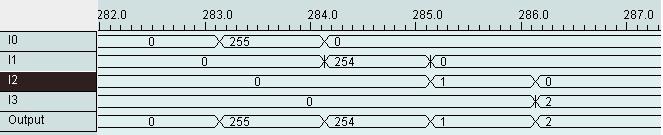
2 2 The 4 to 1 MUX uses two selector bits to determine which 8 bit value is passed through. In order to implement this design, two sub designs were created. The first is an 8 bit Enabler, and the second is, for lack of a better name, the 8 bit MUX Merger. The function of both of these will be explained later. Essentially, though, the decoder works with four enablers to determine which values are allowed through. Since the decoder will have only a single output with 1, and the rest 0, only one of the enablers allows the original value of the bus through, while the rest output 0. All four busses then enter the MUX Merger and are consolidated to a single bus that outputs one of the original values. Instead of testing every 8 bit value combination across 4 busses, I have done the following to show the effectiveness of the MUX. First, I set each 8 bit bus to values that are not equal to each other; then I use all four selector combinations in order to show which bus s value is allowed through the MUX. Simplified Output Table S1 S0 Output Point on Waveform 0 0 I0 Beginning 0 1 I I I SOURCES: Logic and Computer Design Fundamentals Class Notes

3 1B 8 bit Enabler 3
4 4 The 8 bit Enabler takes an 8 bit input and a 1 bit enable. Using 8 logical AND gates, the enabler outputs the original 8 bit number only if the 1 bit enable is true. In the original design, four of these enablers are used with a decoder. One of the four busses would be the input on this circuit, as well as one of the outputs from the decoder. Since only one output works at a time from the decoder, only one of the four 8 bit busses would pass through. The value of the 8 bit input makes no difference on how the circuit functions, so I ve decided to use only four test cases, which are as follows: Simplified Output Table Input Enable Output Point on Waveform Beginning SOURCES: Logic and Computer Design Fundamentals Class Notes

5 8 bit MUX Merger 5
6 6 I had trouble naming this one. It doesn t actually function as an 8 bit logical OR. Its purpose is to take all four 8 bit busses and compare all of their equivalent bits with OR gates; however, only one of the inputs will have a value that isn t 0. Therefore, the real purpose of this sub design is to take all four busses, determine which one has a value, and pass it as a single bus. Once again, the value of the input busses makes no difference on the outcome. The value of whichever bus that has one is the only value that will pass through. I0 I1 I2 I3 Output Point on Waveform Beginning SOURCES: Logic and Computer Design Fundamentals

7 2A 8 bit Adder 7
8 8 The 8 bit adder takes two 8 bit values and outputs the sum of those values. This circuit also takes a carry in, which adds 1 to the value. If the sum exceeds the maximum the 8 bit value can output (255), it also outputs a single bit signifying this and the sum starts from zero again. Therefore, would output 0 and a C_Out bit (signifying 256). Specifically, this is a ripple carry adder. An alternative solution would be a carry look ahead adder. The ripple carry design is slower, but much simpler, whereas the carry look ahead is faster, but more complicated. In this case, I chose to use a simpler design. Once again, instead of doing all possible test cases, I decided to give the few interesting ones that showcase the circuit working as intended. A_In B_In C_In Y_Out C_Out Point on Waveform Beginning ~ ~ ~ ~ ~ ~ ~ ~ ~ ~ ~ ~ ~ ~395 SOURCES: Logic and Computer Design Fundamentals

9 2B Full Adder 9
10 10 The full adder accepts 3 bits as input and outputs two. The inputs A_In and B_In represent two bits of equal significance. The last input, C_In, represents a carry from a sum of lower significance. The output S_Out represents the sum of the bits, and C_Out is used as a carry to another adder of higher significance. 8 of these are used to make an 8 bit Ripple Carry Adder. The logic is simple, just refer to the truth table. A_In B_In C_In S_Out C_Out Point on Waveform Beginning SOURCES: Logic and Computer Design Fundamentals
EXPERIMENT #8: BINARY ARITHMETIC OPERATIONS
 EE 2 Lab Manual, EE Department, KFUPM EXPERIMENT #8: BINARY ARITHMETIC OPERATIONS OBJECTIVES: Design and implement a circuit that performs basic binary arithmetic operations such as addition, subtraction,
5 Arithmetic Logic Unit
 Arithmetic Logic Unit, Muxes 5 Arithmetic Logic Unit I Overview An Arithmetic Logic Unit (ALU) allows many pre-defined functions to be implemented on two binary inputs. We will look at a simple ALU that
Revision: August 31, E Main Suite D Pullman, WA (509) Voice and Fax
 Voice and Fax") Exercise 7: Combinational rithmetic Circuits Revision: ugust 3, 29 25 E Main uite D Pullman, W 9963 (59) 334 636 Voice and Fax TUDENT I am submitting my own work, and I understand penalties will be assessed
Exercise 7: Combinational rithmetic Circuits Revision: ugust 3, 29 25 E Main uite D Pullman, W 9963 (59) 334 636 Voice and Fax TUDENT I am submitting my own work, and I understand penalties will be assessed
Real Digital Problem Set #6
 Real igital Problem et #6. (2 points) ketch a block diagram for a magnitude comparator bit-slice circuit. Create K-maps to define the bit-slice circuit, and use them to find optimal logic equations. ketch
11.1. Unit 11. Adders & Arithmetic Circuits
 . Unit s & Arithmetic Circuits .2 Learning Outcomes I understand what gates are used to design half and full adders I can build larger arithmetic circuits from smaller building blocks ADDER.3 (+) Register.4
Arithmetic Circuits. Nurul Hazlina Adder 2. Multiplier 3. Arithmetic Logic Unit (ALU) 4. HDL for Arithmetic Circuit
 4. HDL for Arithmetic Circuit") Nurul Hazlina 1 1. Adder 2. Multiplier 3. Arithmetic Logic Unit (ALU) 4. HDL for Arithmetic Circuit Nurul Hazlina 2 Introduction 1. Digital circuits are frequently used for arithmetic operations 2. Fundamental
Nurul Hazlina 1 1. Adder 2. Multiplier 3. Arithmetic Logic Unit (ALU) 4. HDL for Arithmetic Circuit Nurul Hazlina 2 Introduction 1. Digital circuits are frequently used for arithmetic operations 2. Fundamental
EET 1131 Lab #7 Arithmetic Circuits
 Name Equipment and Components Safety glasses ETS-7000 Digital-Analog Training System Integrated Circuits: 7483, 74181 Quartus II software and Altera DE2-115 board Multisim simulation software EET 1131
Fundamentals of Computer Systems
 Fundamentals of Computer Systems Combinational Logic Martha. Kim Columbia University Spring 6 / Combinational Circuits Combinational circuits are stateless. Their output is a function only of the current
One and a half hours. Section A is COMPULSORY UNIVERSITY OF MANCHESTER SCHOOL OF COMPUTER SCIENCE
 One and a half hours Section A is COMPULSORY UNIVERSITY OF MANCHESTER SCHOOL OF COMPUTER SCIENCE Fundamentals of Computer Engineering Date: Thursday 21st January 2016 Time: 14:00-15:30 Answer BOTH Questions
CO Computer Architecture and Programming Languages CAPL. Lecture 9
 CO20-320241 Computer Architecture and Programming Languages CAPL Lecture 9 Dr. Kinga Lipskoch Fall 2017 A Four-bit Number Circle CAPL Fall 2017 2 / 38 Functional Parts of an ALU CAPL Fall 2017 3 / 38 Addition
 UNIT II - COMBINATIONAL LOGIC Part A 2 Marks. 1. Define Combinational circuit A combinational circuit consist of logic gates whose outputs at anytime are determined directly from the present combination
Experiment 7 Arithmetic Circuits Design and Implementation
 Experiment 7 Arithmetic Circuits Design and Implementation Introduction: Addition is just what you would expect in computers. Digits are added bit by bit from right to left, with carries passed to the
Lab 0: Introduction to the FPGA Development Board
 Lab 0: Introduction to the FPGA Development Board University of California, Berkeley Department of Electrical Engineering and Computer Sciences EECS150 Components and Design Techniques for Digital Systems
What s a Tri-state Buffer?
 What s a Tri-state Buffer? 2003 by Charles C. Lin. All rights reserved. Introduction Before we talk about tri-state buffers, let s talk about an inverter. You can read about inverters in the notes about
EXPERIMENT NUMBER 11 REGISTERED ALU DESIGN
 11-1 EXPERIMENT NUMBER 11 REGISTERED ALU DESIGN Purpose Extend the design of the basic four bit adder to include other arithmetic and logic functions. References Wakerly: Section 5.1 Materials Required
We are quite familiar with adding two numbers in decimal
 Addition We are quite familiar with adding two numbers in decimal What about adding two binary numbers? If we use the two s complement method to represent binary numbers, addition can be done in a straightforward
EECS150: Components and Design Techniques for Digital Systems
 EECS150: Components and Design Techniques for Digital Systems University of California Dept. of Electrical Engineering and Computer Sciences Midterm 3 Fall 2004 Last name: First name Student ID: Login:
Chapter 3 Arithmetic for Computers
 Chapter 3 Arithmetic for Computers 1 Arithmetic Where we've been: Abstractions: Instruction Set Architecture Assembly Language and Machine Language What's up ahead: Implementing the Architecture operation
Chapter 2 Basic Logic Circuits and VHDL Description
 Chapter 2 Basic Logic Circuits and VHDL Description We cannot solve our problems with the same thinking we used when we created them. ----- Albert Einstein Like a C or C++ programmer don t apply the logic.
EMT1250 LABORATORY EXPERIMENT. EXPERIMENT # 10: Implementing Binary Adders. Name: Date:
 EXPERIMENT # 10: Implementing Binary Adders Name: Date: Equipment/Parts Needed: PC (Altera Quartus II V9.1 installed) DE-2 board Objective: Design a half adder by extracting the Boolean equation from a
DLD VIDYA SAGAR P. potharajuvidyasagar.wordpress.com. Vignana Bharathi Institute of Technology UNIT 3 DLD P VIDYA SAGAR
 DLD UNIT III Combinational Circuits (CC), Analysis procedure, Design Procedure, Combinational circuit for different code converters and other problems, Binary Adder- Subtractor, Decimal Adder, Binary Multiplier,
Name EGR 2131 Lab #6 Number Representation and Arithmetic Circuits
 Name EGR 2131 Lab #6 Number Representation and Arithmetic Circuits Equipment and Components Quartus software and Altera DE2-115 board PART 1: Number Representation in Microsoft Calculator. First, let s
EXPERIMENT NUMBER 7 HIERARCHICAL DESIGN OF A FOUR BIT ADDER (EDA-2)
") 7-1 EXPERIMENT NUMBER 7 HIERARCHICAL DESIGN OF A FOUR BIT ADDER (EDA-2) Purpose The purpose of this exercise is to explore more advanced features of schematic based design. In particular you will go through
7-1 EXPERIMENT NUMBER 7 HIERARCHICAL DESIGN OF A FOUR BIT ADDER (EDA-2) Purpose The purpose of this exercise is to explore more advanced features of schematic based design. In particular you will go through
ECE468 Computer Organization & Architecture. The Design Process & ALU Design
 ECE6 Computer Organization & Architecture The Design Process & Design The Design Process "To Design Is To Represent" Design activity yields description/representation of an object -- Traditional craftsman
M.J. Flynn 1. Lecture 6 EE 486. Bit logic. Ripple adders. Add algorithms. Addition. EE 486 lecture 6: Integer Addition
 EE 486 lecture 6: Integer Addition M. J. Flynn Computer Architecture & Arithmetic Group 1 Stanford University Computer Architecture & Arithmetic Group 2 Stanford University Addition The add function is
BUILDING BLOCKS OF A BASIC MICROPROCESSOR. Part 1 PowerPoint Format of Lecture 3 of Book
 BUILDING BLOCKS OF A BASIC MICROPROCESSOR Part PowerPoint Format of Lecture 3 of Book Decoder Tri-state device Full adder, full subtractor Arithmetic Logic Unit (ALU) Memories Example showing how to write
Lecture #21 March 31, 2004 Introduction to Gates and Circuits
 Lecture #21 March 31, 2004 Introduction to Gates and Circuits To this point we have looked at computers strictly from the perspective of assembly language programming. While it is possible to go a great
CMPT 250 : Week 3 (Sept 19 to Sept 26)
") CMPT 250 : Week 3 (Sept 19 to Sept 26) 1. DESIGN FROM FINITE STATE MACHINES (Continued) 1.1. ONE FLIP-FLOP PER STATE METHOD From a state diagram specification, a sequencer can be constructed using the
CMPT 250 : Week 3 (Sept 19 to Sept 26) 1. DESIGN FROM FINITE STATE MACHINES (Continued) 1.1. ONE FLIP-FLOP PER STATE METHOD From a state diagram specification, a sequencer can be constructed using the
Engin 100 (section 250), Winter 2015, Technical Lecture 3 Page 1 of 5. Use pencil!
, Winter 2015, Technical Lecture 3 Page 1 of 5. Use pencil!") Engin 100 (section 250), Winter 2015, Technical Lecture 3 Page 1 of 5 Use pencil! Last time Introduced basic logic and some terms including bus, word, register and combinational logic. Talked about schematic
Engin 100 (section 250), Winter 2015, Technical Lecture 3 Page 1 of 5 Use pencil! Last time Introduced basic logic and some terms including bus, word, register and combinational logic. Talked about schematic
DIGITAL SYSTEM DESIGN
 DIGITAL SYSTEM DESIGN Prepared By: Engr. Yousaf Hameed Lab Engineer BASIC ELECTRICAL & DIGITAL SYSTEMS LAB DEPARTMENT OF ELECTRICAL ENGINEERING Digital System Design 1 Name: Registration No: Roll No: Semester:
SKEE2263 Sistem Digit
 Term Project Guide SKEE2263 Sistem Digit Table of Contents Objectives... 2 Project Scheduling... 2 Option 1: Serial Multiplier... 3 Option 2 : Serial Divider... 7 Option 3 : GCD Calculator... 11 Option
Department of Computer Science & Engineering. Lab Manual DIGITAL LAB. Class: 2nd yr, 3rd sem SYLLABUS
 Department of Computer Science & Engineering Lab Manual 435 DIGITAL LAB Class: 2nd yr, 3rd sem SYLLABUS. Verification of Boolean theorems using digital logic gates. 2. Design and implementation of code
ENEE 245 Lab 1 Report Rubrics
 ENEE 4 Lab 1 Report Rubrics Design Clearly state the design requirements Derive the minimum SOP Show the circuit implementation. Draw logic diagram and wiring diagram neatly Label all the diagrams/tables
ALU Design. 1-bit Full Adder 4-bit Arithmetic circuits. Arithmetic and Logic Unit Flags. Add/Subtract/Increament/Decrement Circuit
 LU Design -bit Full dder 4-bit rithmetic circuits dd/subtract/increament/decrement Circuit rithmetic and Logic Unit Flags Carry-Out, Sign, Zero, Overflow Shift and Rotate t Operations COE2 (Fall27) LU
Parallel logic circuits
 Computer Mathematics Week 9 Parallel logic circuits College of Information cience and Engineering Ritsumeikan University last week the mathematics of logic circuits the foundation of all digital design
Henry Lin, Department of Electrical and Computer Engineering, California State University, Bakersfield Lecture 7 (Digital Logic) July 24 th, 2012
 July 24 th, 2012") Henry Lin, Department of Electrical and Computer Engineering, California State University, Bakersfield Lecture 7 (Digital Logic) July 24 th, 2012 1 Digital vs Analog Digital signals are binary; analog
Henry Lin, Department of Electrical and Computer Engineering, California State University, Bakersfield Lecture 7 (Digital Logic) July 24 th, 2012 1 Digital vs Analog Digital signals are binary; analog
Lecture 21: Combinational Circuits. Integrated Circuits. Integrated Circuits, cont. Integrated Circuits Combinational Circuits
 Lecture 21: Combinational Circuits Integrated Circuits Combinational Circuits Multiplexer Demultiplexer Decoder Adders ALU Integrated Circuits Circuits use modules that contain multiple gates packaged
Digital Systems Design
 Digital Systems Design Review of Combinatorial Circuit Building Blocks: VHDL for Combinational Circuits Dr. D. J. Jackson Lecture 2-1 Introduction to VHDL Designer writes a logic circuit description in
Computer Architecture Set Four. Arithmetic
 Computer Architecture Set Four Arithmetic Arithmetic Where we ve been: Performance (seconds, cycles, instructions) Abstractions: Instruction Set Architecture Assembly Language and Machine Language What
Digital Fundamentals. Lab 6 2 s Complement / Digital Calculator
 Richland College Engineering Technology Rev. 0. Donham Rev. 1 (7/2003) J. Horne Rev. 2 (1/2008) J. radbury Digital Fundamentals CETT 1425 Lab 6 2 s Complement / Digital Calculator Name: Date: Objectives:
Lab 0: Introduction to the FPGA Development Board
 Lab 0: Introduction to the FPGA Development Board University of California, Berkeley Department of Electrical Engineering and Computer Sciences EECS150 Components and Design Techniques for Digital Systems
Date Performed: Marks Obtained: /10. Group Members (ID):. Experiment # 09 MULTIPLEXERS
:. Experiment # 09 MULTIPLEXERS") Name: Instructor: Engr. Date Performed: Marks Obtained: /10 Group Members (ID):. Checked By: Date: Experiment # 09 MULTIPLEXERS OBJECTIVES: To experimentally verify the proper operation of a multiplexer.
Name: Instructor: Engr. Date Performed: Marks Obtained: /10 Group Members (ID):. Checked By: Date: Experiment # 09 MULTIPLEXERS OBJECTIVES: To experimentally verify the proper operation of a multiplexer.
DIGITAL TECHNICS. Dr. Bálint Pődör. Óbuda University, Microelectronics and Technology Institute
 DIGITAL TECHNIC Dr. Bálint Pődör Óbuda University, Microelectronics and Technology Institute 4. LECTURE: COMBINATIONAL LOGIC DEIGN: ARITHMETIC (THROUGH EXAMPLE) 2nd (Autumn) term 28/29 COMBINATIONAL LOGIC
EET2141 Project 2: Binary Adder Using Xilinx 7.1i Due Friday April 25
 EET2141 Project 2: Binary Adder Using Xilinx 7.1i Due Friday April 25 Introduction This Xilinx project introduces the characteristics of the ripple carry adder. From the last project, you learned that
CS 31: Intro to Systems Digital Logic. Kevin Webb Swarthmore College February 3, 2015
 CS 31: Intro to Systems Digital Logic Kevin Webb Swarthmore College February 3, 2015 Reading Quiz Today Hardware basics Machine memory models Digital signals Logic gates Circuits: Borrow some paper if
Department of Electrical Engineering McGill University ECSE 221 Introduction to Computer Engineering Assignment 2 Combinational Logic
 Department of Electrical Engineering McGill University ECSE 221 Introduction to Computer Engineering Assignment 2 Combinational Logic Question 1: Due October 19 th, 2009 A convenient shorthand for specifying
CMPE 413/ CMSC 711. Project Specification: 16 bit 2 s complement Adder and 8 bit 2 s complement multiplier. GND. Input bus. Latches I[8]-I[15]
![CMPE 413/ CMSC 711. Project Specification: 16 bit 2 s complement Adder and 8 bit 2 s complement multiplier. GND. Input bus. Latches I[8]-I[15]](/thumbs/72/67338890.jpg "CMPE 413/ CMSC 711. Project Specification: 16 bit 2 s complement Adder and 8 bit 2 s complement multiplier. GND. Input bus. Latches I[8]-I[15]") Project Specification: 16 bit 2 s complement Adder and 8 bit 2 s complement multiplier. Assigned: Fri, Nov 3rd Due: Tue, Dec. 19th Description: con1 I[15] I[14] I[13] GND I[12] I[11] I[10] I[9] con2 O[15]
Project Specification: 16 bit 2 s complement Adder and 8 bit 2 s complement multiplier. Assigned: Fri, Nov 3rd Due: Tue, Dec. 19th Description: con1 I[15] I[14] I[13] GND I[12] I[11] I[10] I[9] con2 O[15]
Digital Circuit Design and Language. Datapath Design. Chang, Ik Joon Kyunghee University
 Digital Circuit Design and Language Datapath Design Chang, Ik Joon Kyunghee University Typical Synchronous Design + Control Section : Finite State Machine + Data Section: Adder, Multiplier, Shift Register
CS 31: Intro to Systems Digital Logic. Kevin Webb Swarthmore College February 2, 2016
 CS 31: Intro to Systems Digital Logic Kevin Webb Swarthmore College February 2, 2016 Reading Quiz Today Hardware basics Machine memory models Digital signals Logic gates Circuits: Borrow some paper if
VHDL 2 Combinational Logic Circuits. Reference: Roth/John Text: Chapter 2
 VHDL 2 Combinational Logic Circuits Reference: Roth/John Text: Chapter 2 Combinational logic -- Behavior can be specified as concurrent signal assignments -- These model concurrent operation of hardware
Fundamentals of Computer Systems
 Fundamentals of Computer Systems Combinational Logic Stephen. Edwards Columbia University Summer 7 Combinational Circuits Combinational circuits are stateless. Their output is a function only of the current
CSE 140L Final Exam. Prof. Tajana Simunic Rosing. Spring 2008
 CSE 140L Final Exam Prof. Tajana Simunic Rosing Spring 2008 NAME: ID#: Do not start the exam until you are told to. Turn off any cell phones or pagers. Write your name and PID at the top of every page.
Lecture 2: Data Types, Modeling Combinational Logic in Verilog HDL. Variables and Logic Value Set. Data Types. Why use an HDL?
 Why use an HDL? Lecture 2: Data Types, Modeling Combinational Logic in Verilog HDL Increase digital design engineer s productivity (from Dataquest) Behavioral HDL RTL HDL Gates Transistors 2K 10K gates/week
VLSI Final Project: Alarm Clock
 Jason Fong William Durley 4-11-01 VLSI Final Project: Alarm Clock Functional Overview The goal of this project was the design of a 24-hour alarm clock. Our chip consists of two major sections. The first
CS Computer Architecture. 1. Explain Carry Look Ahead adders in detail
 1. Explain Carry Look Ahead adders in detail A carry-look ahead adder (CLA) is a type of adder used in digital logic. A carry-look ahead adder improves speed by reducing the amount of time required to
CCE 3202 Advanced Digital System Design
 CCE 3202 Advanced Digital System Design Lab Exercise #2 Introduction You will use Xilinx Webpack v9.1 to allow the synthesis and creation of VHDLbased designs. This lab will outline the steps necessary
COE 405, Term 062. Design & Modeling of Digital Systems. HW# 1 Solution. Due date: Wednesday, March. 14
 COE 405, Term 062 Design & Modeling of Digital Systems HW# 1 Solution Due date: Wednesday, March. 14 Q.1. Consider the 4-bit carry-look-ahead adder (CLA) block shown below: A 3 -A 0 B 3 -B 0 C 3 4-bit
CS 31: Intro to Systems Digital Logic
 CS 3: Intro to Systems Digital Logic Martin Gagné Swarthmore College January 3, 27 You re going to want scratch papr today borrow some if needed. Quick nnouncements Late Policy Reminder 3 late days total
Debouncing a Switch. A Design Example. Page 1
 Debouncing a Switch A Design Example Page 1 Background and Motivation Page 2 When you throw a switch (button or two-pole switch) It often bounces Page 3 Another switch switch after inversion Page 4 Yet
637 has a 1 s place, 10 s place and 100 s place Show how to go from *256+7* =
 1 3 4 637 has a 1 s place, 10 s place and 100 s place Show how to go from 512+64+32+16+8+4+1 512+64+56+5 2*256+7*16+ 13 = 512+112+13 5 The base represents the number of unique symbols (decimal has 10,
Chapter 1. Microprocessor architecture ECE Dr. Mohamed Mahmoud.
 Chapter 1 Microprocessor architecture ECE 3130 Dr. Mohamed Mahmoud The slides are copyright protected. It is not permissible to use them without a permission from Dr Mahmoud http://www.cae.tntech.edu/~mmahmoud/
Question Total Possible Test Score Total 100
 Computer Engineering 2210 Final Name 11 problems, 100 points. Closed books, closed notes, no calculators. You would be wise to read all problems before beginning, note point values and difficulty of problems,
ECE 448 Lecture 3. Combinational-Circuit Building Blocks. Data Flow Modeling of Combinational Logic
 ECE 448 Lecture 3 Combinational-Circuit Building Blocks Data Flow Modeling of Combinational Logic George Mason University Reading Required P. Chu, FPGA Prototyping by VHDL Examples Chapter 3, RT-level
Chapter 4. Combinational Logic
 Chapter 4. Combinational Logic Tong In Oh 1 4.1 Introduction Combinational logic: Logic gates Output determined from only the present combination of inputs Specified by a set of Boolean functions Sequential
ECE 448 Lecture 3. Combinational-Circuit Building Blocks. Data Flow Modeling of Combinational Logic
 ECE 448 Lecture 3 Combinational-Circuit Building Blocks Data Flow Modeling of Combinational Logic George Mason University Reading Required P. Chu, FPGA Prototyping by VHDL Examples Chapter 3, RT-level
CAD4 The ALU Fall 2009 Assignment. Description
 CAD4 The ALU Fall 2009 Assignment To design a 16-bit ALU which will be used in the datapath of the microprocessor. This ALU must support two s complement arithmetic and the instructions in the baseline
EGCP 1010 Digital Logic Design (DLD) Laboratory #6
 Laboratory #6") EGCP 11 Digital Logic Design (DLD) Laboratory #6 Four by Four (4 x 4) Sorting Stack Prepared By: Alex Laird on October 1st, 2 Lab Partner: Ryan Morehart Objective: The goal of this laboratory is to expose
EGCP 11 Digital Logic Design (DLD) Laboratory #6 Four by Four (4 x 4) Sorting Stack Prepared By: Alex Laird on October 1st, 2 Lab Partner: Ryan Morehart Objective: The goal of this laboratory is to expose
ECEN 468 Advanced Logic Design
 ECEN 468 Advanced Logic Design Lecture 26: Verilog Operators ECEN 468 Lecture 26 Operators Operator Number of Operands Result Arithmetic 2 Binary word Bitwise 2 Binary word Reduction 1 Bit Logical 2 Boolean
Area Efficient, Low Power Array Multiplier for Signed and Unsigned Number. Chapter 3
 Area Efficient, Low Power Array Multiplier for Signed and Unsigned Number Chapter 3 Area Efficient, Low Power Array Multiplier for Signed and Unsigned Number Chapter 3 3.1 Introduction The various sections
A Brief Introduction to Verilog Hardware Definition Language (HDL)
") www.realdigital.org A Brief Introduction to Verilog Hardware Definition Language (HDL) Forward Verilog is a Hardware Description language (HDL) that is used to define the structure and/or behavior of digital
www.realdigital.org A Brief Introduction to Verilog Hardware Definition Language (HDL) Forward Verilog is a Hardware Description language (HDL) that is used to define the structure and/or behavior of digital
Logic Design (Part 2) Combinational Logic Circuits (Chapter 3)
 Combinational Logic Circuits (Chapter 3)") Digital Logic Circuits Logic Design (Part ) Combinational Logic Circuits (Chapter 3) ² We saw how we can build the simple logic gates using transistors ² Use these gates as building blocks to build more
Digital Logic Circuits Logic Design (Part ) Combinational Logic Circuits (Chapter 3) ² We saw how we can build the simple logic gates using transistors ² Use these gates as building blocks to build more
1. What is y-chart? ans: The y- chart consists of three domains:- behavioral, structural and geometrical.
 SECTION- A Short questions: (each 2 marks) 1. What is y-chart? ans: The y- chart consists of three domains:- behavioral, structural and geometrical. 2. What is fabrication? ans: It is the process used
Altera Quartus II Tutorial
 Altera Quartus II Tutorial Part II (For ECE 465 Students at UIC) Sajjad Rahaman TA for ECE 465, Spring 2009 Department of Electrical and Computer Engineering University of Illinois at Chicago mrahaman@ece.uic.edu
VALLIAMMAI ENGINEERING COLLEGE. SRM Nagar, Kattankulathur DEPARTMENT OF ELECTRONICS AND COMMUNICATION ENGINEERING EC6302 DIGITAL ELECTRONICS
 VALLIAMMAI ENGINEERING COLLEGE SRM Nagar, Kattankulathur-603 203 DEPARTMENT OF ELECTRONICS AND COMMUNICATION ENGINEERING EC6302 DIGITAL ELECTRONICS YEAR / SEMESTER: II / III ACADEMIC YEAR: 2015-2016 (ODD
COMPSCI 210 S Computer Systems 1. 6 Sequential Logic Circuit
 COMPSCI 2 S2 27 Computer Systems 6 Sequential Logic Circuit Overview Basic sequential logic circuit Latches Registers Memory Finite state machine 2 Building Functions from Logic Gates Combinational logic
Experiment # 5 Debugging via Simulation using epd
 1. Synopsis: Experiment # 5 Debugging via Simulation using epd In this lab you will be debugging an arbitrary design. We have introduced different kinds of errors in the design purposefully to demonstrate
CS6201-DIGITAL PRINCIPLE AND SYSTEM DESIGN I YEAR/II SEM PART-B UNIT-I BOOLEAN ALGEBRA AND LOGIC GATES.
 CS6201-DIGITAL PRINCIPLE AND SYSTEM DESIGN I YEAR/II SEM PART-B UNIT-I BOOLEAN ALGEBRA AND LOGIC GATES. 1) Simplify the boolean function using tabulation method. F = (0, 1, 2, 8, 10, 11, 14, 15) List all
Chapter 6 Combinational-Circuit Building Blocks
 Chapter 6 Combinational-Circuit Building Blocks Commonly used combinational building blocks in design of large circuits: Multiplexers Decoders Encoders Comparators Arithmetic circuits Multiplexers A multiplexer
 CS6303 COMPUTER ARCHITECTURE LESSION NOTES UNIT II ARITHMETIC OPERATIONS ALU In computing an arithmetic logic unit (ALU) is a digital circuit that performs arithmetic and logical operations. The ALU is
CSE 140L Final Exam. Prof. Tajana Simunic Rosing. Spring 2008
 CSE 140L Final Exam Prof. Tajana Simunic Rosing Spring 2008 Do not start the exam until you are told to. Turn off any cell phones or pagers. Write your name and PID at the top of every page. Do not separate
Chapter 5 Registers & Counters
 University of Wisconsin - Madison ECE/Comp Sci 352 Digital Systems Fundamentals Kewal K. Saluja and Yu Hen Hu Spring 2002 Chapter 5 Registers & Counters Originals by: Charles R. Kime Modified for course
Lec-6-HW-2-digitalDesign
 Lec-6-HW-2-digitalDesign Reading: PP-chp 3: 3.3 (decoder, mux, FA, PLA) 3.4 (R-S latch, register) 3.5 (memory) 3.6 (sequential machines, FSM) 3.7 (LC-3 datapath) Problems, PP-chp 3: 3.12 3-Dec, show minterm
Declarations of Components and Entities are similar Components are virtual design entities entity OR_3 is
 Reserved Words component OR_3 port (A,B,C: in bit; Z: out bit); end component ; Reserved Words Declarations of Components and Entities are similar Components are virtual design entities entity OR_3 is
Solution printed. Do not start the test until instructed to do so! CS 2504 Intro Computer Organization Test 2 Spring 2006.
 VIRG INIA POLYTECHNIC INSTITUTE AND STATE U T PROSI M UNI VERSI TY Instructions: Print your name in the space provided below. This examination is closed book and closed notes, aside from the permitted
ELCT 501: Digital System Design
 ELCT 501: Digital System Lecture 4: CAD tools (Continued) Dr. Mohamed Abd El Ghany, Basic VHDL Concept Via an Example Problem: write VHDL code for 1-bit adder 4-bit adder 2 1-bit adder Inputs: A (1 bit)
HANSABA COLLEGE OF ENGINEERING & TECHNOLOGY (098) SUBJECT: DIGITAL ELECTRONICS ( ) Assignment
 SUBJECT: DIGITAL ELECTRONICS ( ) Assignment") Assignment 1. What is multiplexer? With logic circuit and function table explain the working of 4 to 1 line multiplexer. 2. Implement following Boolean function using 8: 1 multiplexer. F(A,B,C,D) = (2,3,5,7,8,9,12,13,14,15)
Assignment 1. What is multiplexer? With logic circuit and function table explain the working of 4 to 1 line multiplexer. 2. Implement following Boolean function using 8: 1 multiplexer. F(A,B,C,D) = (2,3,5,7,8,9,12,13,14,15)
CSE140 L. Instructor: Thomas Y. P. Lee January 18,2006. CSE140L Course Info
 CSE4 L Instructor: Thomas Y. P. Lee January 8,26 CSE4L Course Info Lectures Wedesday :-:2AM, HSS33 Lab Assignment egins TA s JinHua Liu (jhliu@cs.ucsd.edu) Contact TAs if you re still looking for a lab
Finite-State Machine (FSM) Design
 Design") 1 Finite-State Machine (FSM) Design FSMs, an important category of sequential circuits, are used frequently in designing digital systems. From the daily used electronic machines to the complex digital
1 Finite-State Machine (FSM) Design FSMs, an important category of sequential circuits, are used frequently in designing digital systems. From the daily used electronic machines to the complex digital
CS 261 Fall Mike Lam, Professor. Combinational Circuits
 CS 261 Fall 2017 Mike Lam, Professor Combinational Circuits The final frontier Java programs running on Java VM C programs compiled on Linux Assembly / machine code on CPU + memory??? Switches and electric
Chap 6 Introduction to HDL (d)
") Design with Verilog Chap 6 Introduction to HDL (d) Credit to: MD Rizal Othman Faculty of Electrical & Electronics Engineering Universiti Malaysia Pahang Ext: 6036 VERILOG HDL Basic Unit A module Module
Design with Verilog Chap 6 Introduction to HDL (d) Credit to: MD Rizal Othman Faculty of Electrical & Electronics Engineering Universiti Malaysia Pahang Ext: 6036 VERILOG HDL Basic Unit A module Module
ANADOLU UNIVERSITY DEPARTMENT OF ELECTRICAL AND ELECTRONICS ENGINEERING. EEM Digital Systems II
 ANADOLU UNIVERSITY DEPARTMENT OF ELECTRICAL AND ELECTRONICS ENGINEERING EEM 334 - Digital Systems II LAB 1 - INTRODUCTION TO XILINX ISE SOFTWARE AND FPGA 1. PURPOSE In this lab, after you learn to use
EE 8351 Digital Logic Circuits Ms.J.Jayaudhaya, ASP/EEE
 EE 8351 Digital Logic Circuits Ms.J.Jayaudhaya, ASP/EEE 1 Logic circuits for digital systems may be combinational or sequential. A combinational circuit consists of input variables, logic gates, and output
Note that none of the above MAY be a VALID ANSWER.
 ECE 270 Learning Outcome 4-1 - Practice Exam / Solution OUTCOME #4: An ability to design and implement computer logic circuits. Multiple Choice select the single most appropriate response for each question.
Combinational Logic with MSI and LSI
 1010101010101010101010101010101010101010101010101010101010101010101010101010101010 1010101010101010101010101010101010101010101010101010101010101010101010101010101010 1010101010101010101010101010101010101010101010101010101010101010101010101010101010
EE878 Special Topics in VLSI. Computer Arithmetic for Digital Signal Processing
 EE878 Special Topics in VLSI Computer Arithmetic for Digital Signal Processing Part 6b High-Speed Multiplication - II Spring 2017 Koren Part.6b.1 Accumulating the Partial Products After generating partial
EE577A FINAL PROJECT REPORT Design of a General Purpose CPU
 EE577A FINAL PROJECT REPORT Design of a General Purpose CPU Submitted By Youngseok Lee - 4930239194 Narayana Reddy Lekkala - 9623274062 Chirag Ahuja - 5920609598 Phase 2 Part 1 A. Introduction The core
Combinational Circuits
 Combinational Circuits Combinational circuit consists of an interconnection of logic gates They react to their inputs and produce their outputs by transforming binary information n input binary variables
CMPT 250: Computer Architecture. Using LogicWorks 5. Tutorial Part 1. Somsubhra Sharangi
 CMPT 250: Computer Architecture Using LogicWorks 5 Tutorial Part 1 Somsubhra Sharangi What is VHDL? A high level language to describe digital circuit Different that a programming language ( such as Java)
Engineering 303 Digital Logic Design Fall 2018
 Engineering 303 Digital Logic Design Fall 2018 LAB 4: Seven Seg, Full Adder, Ripple Adder, Heirarchical Design Build the following designs and verify correct operation. This lab uses hierarchical design.
Numbering Systems. Number Representations Part 1
 Introduction Verilog HDL modeling language allows numbers being represented in several radix systems. The underlying circuit processes the number in binary, however, input into and output from such circuits