Department of Electrical Engineering McGill University ECSE 221 Introduction to Computer Engineering Assignment 2 Combinational Logic
|
|
|
- Brandon Johns
- 5 years ago
- Views:
Transcription
1 Department of Electrical Engineering McGill University ECSE 221 Introduction to Computer Engineering Assignment 2 Combinational Logic Question 1: Due October 19 th, 2009 A convenient shorthand for specifying truth tables is to list the set of minterms (or maxterms) for which the corresponding Boolean function is true (or false). Consider the following truth table: A B C D F(A,B,C,D) d d F(A, B,C, D) = F(A, B,C, D) = 1 d 0 d 2,3, 5,10,11,13 + 0,8 1,4,6,7,9,12,14,15 + 0,8 The shorthand for the sum-of-products ( ) and product-of-sums ( ) forms is shown at the right of the truth table. Given this specification for a Boolean function, answer the following questions. a) Use algebraic methods to derive the minimal forms for both and assuming that don't cares are set to 0 for and 1 for. b) Repeat the above using Karnaugh maps. Here you may choose the don't cares to minimize the resulting expressions. c) Repeat the minimization, this time assuming don't cares are all 0, using any minimization method. Prove algebraically that the resulting forms are equal (same truth table).
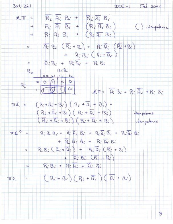
2 Question 2 Write down the truth table for a full subtracter. Your truth table should be laid out in the following order: R i A i B i D i R o The structure is identical to that of the full adder, except that D i corresponds to the difference, R i to the borrow input, and R o to the borrow output respectively. In a non two's complement machine such a circuit would be required to implement the subtraction operation directly. Once you have determined the truth table, determine the minimal and forms corresponding to the borrow output, R o, respectively. Do this using both algebraic minimization and Karnaugh maps. Implement the corresponding circuits using NAND-NAND and NOR-NOR logic in LogicWorks. Show that your circuits implement the specified truth tables. Question 3 Any Boolean function can be implemented using either NAND gates or NOR gates exclusively, provided that sufficient inputs are available (e.g. a 4-input NAND gate can serve as a 3-input NAND gate, a 2-input NAND gate, and an inverter). Determine the maximum number of inputs for each of the circuits you designed in Question 2 and design the corresponding gates following the examples shown in the course notes. For this question use active pull-ups and pull-downs. Implement and test your gates using LogicWorks. You can then use the DEVICE SYMBOL option under the FILE menu to encapsulate your gate design for subsequent use. Test each of the 2 gates using LogicWorks (i.e. verify their truth tables). Next, re-implement each of the two circuits from Question 2 (NAND-NAND and NOR-NOR), and verify their functionality using the same testing as applied in Question 2. Note: Since LogicWorks does not have an active(0) type of switch, use an inverter connected to the control input of an active(1) switch instead. If you want to be a bit more elegant, use the device editor to create an active(0) switch by modifying the active(1) switch (i.e. X-gate) by negating the control input. You can also use the drawing tools to place an inverter bubble on the gate symbol. MAKE SURE THAT YOU SAVE THE RESULT IN A DIFFERENT LIBRARY UNDER A DIFFERENT NAME so that you don't overwrite the existing part.
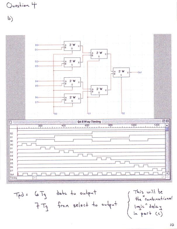
3 Question 4 Another way to implement a truth table is to use a multiplexer. A 2 to1 mux, like the one discussed in class, can select one of two inputs using a single control input. A 4 to 1 mux selects one of four inputs using two control inputs. Consider the following. By using the 2 control inputs as the table input variables and appropriately hard wiring the 4 inputs of the mux to 0 or 1, a 2 input truth table can be implemented. Using this approach, an n input truth table can be implemented using a n 2 to 1 mux. a) Using the gate types you designed in Question 3, design a 2 to 1 multiplexer. Verify its operation using LogicWorks. b) Now using the 2-way routing switch as a building block (use the device editor in LogicWorks to encapsulate the 2-way switch), design a multiplexer large enough to implement the truth table described in Question 2. Predict the propagation delay, T pd, of your multiplexer (you will need this to figure out how to space the inputs to your circuit in time). Test your multiplexer with appropriate waveforms and verify that the measured T pd is consistent with its predicted value. c) Hard wire the inputs to your multiplexer to implement the truth table described in Question 2. Verify its operation using LogicWorks. d) Explain the presence of any anomalous signals (glitches) in your output and give an example of an input transition that results in a glitch at the output. Show this example using LogicWorks. Question 5: Bonus The size of the multiplexer used to implement a truth table can be cut in half (e.g. 4 inputs instead of 8) if one of the variables is used as an input instead of being connected to a select line. For example, a truth table with inputs A, B, C, could be implemented using a 4-input multiplexer with A and B connected to the 2 select lines. A and B would then be able to select 0, 1, C or C (assuming that an inverter is available for C). Figure out how to re-implement Question 3 this way and prove that your solution is correct with a LogicWorks simulation. FPF/October 5 th, 2009
4
5
6
7
8
9
10
11
12
13
14
15
16
17
18
1. Mark the correct statement(s)
") 1. Mark the correct statement(s) 1.1 A theorem in Boolean algebra: a) Can easily be proved by e.g. logic induction b) Is a logical statement that is assumed to be true, c) Can be contradicted by another
1. Mark the correct statement(s) 1.1 A theorem in Boolean algebra: a) Can easily be proved by e.g. logic induction b) Is a logical statement that is assumed to be true, c) Can be contradicted by another
QUESTION BANK FOR TEST
 CSCI 2121 Computer Organization and Assembly Language PRACTICE QUESTION BANK FOR TEST 1 Note: This represents a sample set. Please study all the topics from the lecture notes. Question 1. Multiple Choice
Logic Gates and Boolean Algebra ENT263
 Logic Gates and Boolean Algebra ENT263 Logic Gates and Boolean Algebra Now that we understand the concept of binary numbers, we will study ways of describing how systems using binary logic levels make
Objectives: 1. Design procedure. 2. Fundamental circuits. 1. Design procedure
 Objectives: 1. Design procedure. 2. undamental circuits. 1. Design procedure Design procedure has five steps: o Specification. o ormulation. o Optimization. o Technology mapping. o Verification. Specification:
Chapter 2. Boolean Expressions:
 Chapter 2 Boolean Expressions: A Boolean expression or a function is an expression which consists of binary variables joined by the Boolean connectives AND and OR along with NOT operation. Any Boolean
EXPERIMENT #8: BINARY ARITHMETIC OPERATIONS
 EE 2 Lab Manual, EE Department, KFUPM EXPERIMENT #8: BINARY ARITHMETIC OPERATIONS OBJECTIVES: Design and implement a circuit that performs basic binary arithmetic operations such as addition, subtraction,
B.Tech II Year I Semester (R13) Regular Examinations December 2014 DIGITAL LOGIC DESIGN
 Regular Examinations December 2014 DIGITAL LOGIC DESIGN") B.Tech II Year I Semester () Regular Examinations December 2014 (Common to IT and CSE) (a) If 1010 2 + 10 2 = X 10, then X is ----- Write the first 9 decimal digits in base 3. (c) What is meant by don
B.Tech II Year I Semester () Regular Examinations December 2014 (Common to IT and CSE) (a) If 1010 2 + 10 2 = X 10, then X is ----- Write the first 9 decimal digits in base 3. (c) What is meant by don
Code No: R Set No. 1
 Code No: R059210504 Set No. 1 II B.Tech I Semester Regular Examinations, November 2007 DIGITAL LOGIC DESIGN ( Common to Computer Science & Engineering, Information Technology and Computer Science & Systems
Chapter 3. Gate-Level Minimization. Outlines
 Chapter 3 Gate-Level Minimization Introduction The Map Method Four-Variable Map Five-Variable Map Outlines Product of Sums Simplification Don t-care Conditions NAND and NOR Implementation Other Two-Level
Department of Electrical and Computer Engineering University of Wisconsin - Madison. ECE/CS 352 Digital System Fundamentals.
 Department of Electrical and Computer Engineering University of Wisconsin - Madison ECE/C 352 Digital ystem Fundamentals Quiz #2 Thursday, March 7, 22, 7:15--8:3PM 1. (15 points) (a) (5 points) NAND, NOR
DIGITAL ELECTRONICS. P41l 3 HOURS
 UNIVERSITY OF SWAZILAND FACUL TY OF SCIENCE AND ENGINEERING DEPARTMENT OF PHYSICS MAIN EXAMINATION 2015/16 TITLE OF PAPER: COURSE NUMBER: TIME ALLOWED: INSTRUCTIONS: DIGITAL ELECTRONICS P41l 3 HOURS ANSWER
Combinational Circuits
 Combinational Circuits Combinational circuit consists of an interconnection of logic gates They react to their inputs and produce their outputs by transforming binary information n input binary variables
Experiment 3: Logic Simplification
 Module: Logic Design Name:... University no:.. Group no:. Lab Partner Name: Mr. Mohamed El-Saied Experiment : Logic Simplification Objective: How to implement and verify the operation of the logical functions
Midterm Exam Review. CS 2420 :: Fall 2016 Molly O'Neil
 Midterm Exam Review CS 2420 :: Fall 2016 Molly O'Neil Midterm Exam Thursday, October 20 In class, pencil & paper exam Closed book, closed notes, no cell phones or calculators, clean desk 20% of your final
Gate Level Minimization Map Method
 Gate Level Minimization Map Method Complexity of hardware implementation is directly related to the complexity of the algebraic expression Truth table representation of a function is unique Algebraically
2008 The McGraw-Hill Companies, Inc. All rights reserved.
 28 The McGraw-Hill Companies, Inc. All rights reserved. 28 The McGraw-Hill Companies, Inc. All rights reserved. All or Nothing Gate Boolean Expression: A B = Y Truth Table (ee next slide) or AB = Y 28
Standard Forms of Expression. Minterms and Maxterms
 Standard Forms of Expression Minterms and Maxterms Standard forms of expressions We can write expressions in many ways, but some ways are more useful than others A sum of products (SOP) expression contains:
Combinational Circuits Digital Logic (Materials taken primarily from:
 Combinational Circuits Digital Logic (Materials taken primarily from: http://www.facstaff.bucknell.edu/mastascu/elessonshtml/eeindex.html http://www.cs.princeton.edu/~cos126 ) Digital Systems What is a
COMBINATIONAL LOGIC CIRCUITS
 COMBINATIONAL LOGIC CIRCUITS 4.1 INTRODUCTION The digital system consists of two types of circuits, namely: (i) Combinational circuits and (ii) Sequential circuits A combinational circuit consists of logic
Synthesis of combinational logic
 Page 1 of 14 Synthesis of combinational logic indicates problems that have been selected for discussion in section, time permitting. Problem 1. A certain function F has the following truth table: A B C
Incompletely Specified Functions with Don t Cares 2-Level Transformation Review Boolean Cube Karnaugh-Map Representation and Methods Examples
 Lecture B: Logic Minimization Incompletely Specified Functions with Don t Cares 2-Level Transformation Review Boolean Cube Karnaugh-Map Representation and Methods Examples Incompletely specified functions
Assignment (3-6) Boolean Algebra and Logic Simplification - General Questions
 Boolean Algebra and Logic Simplification - General Questions") Assignment (3-6) Boolean Algebra and Logic Simplification - General Questions 1. Convert the following SOP expression to an equivalent POS expression. 2. Determine the values of A, B, C, and D that make
Assignment (3-6) Boolean Algebra and Logic Simplification - General Questions 1. Convert the following SOP expression to an equivalent POS expression. 2. Determine the values of A, B, C, and D that make
Lecture (05) Boolean Algebra and Logic Gates
 Boolean Algebra and Logic Gates") Lecture (05) Boolean Algebra and Logic Gates By: Dr. Ahmed ElShafee ١ Minterms and Maxterms consider two binary variables x and y combined with an AND operation. Since eachv ariable may appear in either
Lecture (05) Boolean Algebra and Logic Gates By: Dr. Ahmed ElShafee ١ Minterms and Maxterms consider two binary variables x and y combined with an AND operation. Since eachv ariable may appear in either
CS8803: Advanced Digital Design for Embedded Hardware
 CS883: Advanced Digital Design for Embedded Hardware Lecture 2: Boolean Algebra, Gate Network, and Combinational Blocks Instructor: Sung Kyu Lim (limsk@ece.gatech.edu) Website: http://users.ece.gatech.edu/limsk/course/cs883
GC03 Boolean Algebra
 Why study? GC3 Boolean Algebra Computers transfer and process binary representations of data. Binary operations are easily represented and manipulated in Boolean algebra! Digital electronics is binary/boolean
Chapter 2 Boolean algebra and Logic Gates
 Chapter 2 Boolean algebra and Logic Gates 2. Introduction In working with logic relations in digital form, we need a set of rules for symbolic manipulation which will enable us to simplify complex expressions
VALLIAMMAI ENGINEERING COLLEGE. SRM Nagar, Kattankulathur DEPARTMENT OF ELECTRONICS AND COMMUNICATION ENGINEERING EC6302 DIGITAL ELECTRONICS
 VALLIAMMAI ENGINEERING COLLEGE SRM Nagar, Kattankulathur-603 203 DEPARTMENT OF ELECTRONICS AND COMMUNICATION ENGINEERING EC6302 DIGITAL ELECTRONICS YEAR / SEMESTER: II / III ACADEMIC YEAR: 2015-2016 (ODD
Review. EECS Components and Design Techniques for Digital Systems. Lec 05 Boolean Logic 9/4-04. Seq. Circuit Behavior. Outline.
 Review EECS 150 - Components and Design Techniques for Digital Systems Lec 05 Boolean Logic 94-04 David Culler Electrical Engineering and Computer Sciences University of California, Berkeley Design flow
Combinational Logic Circuits
 Chapter 3 Combinational Logic Circuits 12 Hours 24 Marks 3.1 Standard representation for logical functions Boolean expressions / logic expressions / logical functions are expressed in terms of logical
Chapter 6. Logic Design Optimization Chapter 6
 Chapter 6 Logic Design Optimization Chapter 6 Optimization The second part of our design process. Optimization criteria: Performance Size Power Two-level Optimization Manipulating a function until it is
TWO-LEVEL COMBINATIONAL LOGIC
 TWO-LEVEL COMBINATIONAL LOGIC OVERVIEW Canonical forms To-level simplification Boolean cubes Karnaugh maps Quine-McClusky (Tabulation) Method Don't care terms Canonical and Standard Forms Minterms and
HANSABA COLLEGE OF ENGINEERING & TECHNOLOGY (098) SUBJECT: DIGITAL ELECTRONICS ( ) Assignment
 SUBJECT: DIGITAL ELECTRONICS ( ) Assignment") Assignment 1. What is multiplexer? With logic circuit and function table explain the working of 4 to 1 line multiplexer. 2. Implement following Boolean function using 8: 1 multiplexer. F(A,B,C,D) = (2,3,5,7,8,9,12,13,14,15)
Assignment 1. What is multiplexer? With logic circuit and function table explain the working of 4 to 1 line multiplexer. 2. Implement following Boolean function using 8: 1 multiplexer. F(A,B,C,D) = (2,3,5,7,8,9,12,13,14,15)
Gate-Level Minimization. BME208 Logic Circuits Yalçın İŞLER
 Gate-Level Minimization BME28 Logic Circuits Yalçın İŞLER islerya@yahoo.com http://me.islerya.com Complexity of Digital Circuits Directly related to the complexity of the algebraic expression we use to
CS470: Computer Architecture. AMD Quad Core
 CS470: Computer Architecture Yashwant K. Malaiya, Professor malaiya@cs.colostate.edu AMD Quad Core 1 Architecture Layers Building blocks Gates, flip-flops Functional bocks: Combinational, Sequential Instruction
Gate-Level Minimization
 MEC520 디지털공학 Gate-Level Minimization Jee-Hwan Ryu School of Mechanical Engineering Gate-Level Minimization-The Map Method Truth table is unique Many different algebraic expression Boolean expressions may
BUILDING BLOCKS OF A BASIC MICROPROCESSOR. Part 1 PowerPoint Format of Lecture 3 of Book
 BUILDING BLOCKS OF A BASIC MICROPROCESSOR Part PowerPoint Format of Lecture 3 of Book Decoder Tri-state device Full adder, full subtractor Arithmetic Logic Unit (ALU) Memories Example showing how to write
Simplification of Boolean Functions
 COM111 Introduction to Computer Engineering (Fall 2006-2007) NOTES 5 -- page 1 of 5 Introduction Simplification of Boolean Functions You already know one method for simplifying Boolean expressions: Boolean
Chap-2 Boolean Algebra
 Chap-2 Boolean Algebra Contents: My name Outline: My position, contact Basic information theorem and postulate of Boolean Algebra. or project description Boolean Algebra. Canonical and Standard form. Digital
Code No: R Set No. 1
 Code No: R059210504 Set No. 1 II B.Tech I Semester Regular Examinations, November 2006 DIGITAL LOGIC DESIGN ( Common to Computer Science & Engineering, Information Technology and Computer Science & Systems
Dr. S. Shirani COE2DI4 Midterm Test #1 Oct. 14, 2010
 Dr. S. Shirani COE2DI4 Midterm Test #1 Oct. 14, 2010 Instructions: This examination paper includes 9 pages and 20 multiple-choice questions starting on page 3. You are responsible for ensuring that your
Injntu.com Injntu.com Injntu.com R16
 1. a) What are the three methods of obtaining the 2 s complement of a given binary (3M) number? b) What do you mean by K-map? Name it advantages and disadvantages. (3M) c) Distinguish between a half-adder
Combinational Logic Worksheet
 Combinational Logic Worksheet Concept Inventory: Truth tables sum-of-products equations implementation using NOT/AND/OR Demorgan s Law, implementation using NAND/NOR Simplification, truth tables w/ don
CprE 281: Digital Logic
 CprE 28: Digital Logic Instructor: Alexander Stoytchev http://www.ece.iastate.edu/~alexs/classes/ Minimization CprE 28: Digital Logic Iowa State University, Ames, IA Copyright Alexander Stoytchev Administrative
EECS150 Homework 2 Solutions Fall ) CLD2 problem 2.2. Page 1 of 15
 CLD2 problem 2.2. Page 1 of 15") 1.) CLD2 problem 2.2 We are allowed to use AND gates, OR gates, and inverters. Note that all of the Boolean expression are already conveniently expressed in terms of AND's, OR's, and inversions. Thus,
1.) CLD2 problem 2.2 We are allowed to use AND gates, OR gates, and inverters. Note that all of the Boolean expression are already conveniently expressed in terms of AND's, OR's, and inversions. Thus,
Digital logic fundamentals. Question Bank. Unit I
 Digital logic fundamentals Question Bank Subject Name : Digital Logic Fundamentals Subject code: CA102T Staff Name: R.Roseline Unit I 1. What is Number system? 2. Define binary logic. 3. Show how negative
Arithmetic-logic units
 Arithmetic-logic units An arithmetic-logic unit, or ALU, performs many different arithmetic and logic operations. The ALU is the heart of a processor you could say that everything else in the CPU is there
LECTURE 4. Logic Design
 LECTURE 4 Logic Design LOGIC DESIGN The language of the machine is binary that is, sequences of 1 s and 0 s. But why? At the hardware level, computers are streams of signals. These signals only have two
Computer Organization and Levels of Abstraction
 Computer Organization and Levels of Abstraction Announcements PS8 Due today PS9 Due July 22 Sound Lab tonight bring machines and headphones! Binary Search Today Review of binary floating point notation
SWITCHING THEORY AND LOGIC CIRCUITS
 SWITCHING THEORY AND LOGIC CIRCUITS COURSE OBJECTIVES. To understand the concepts and techniques associated with the number systems and codes 2. To understand the simplification methods (Boolean algebra
Parallel logic circuits
 Computer Mathematics Week 9 Parallel logic circuits College of Information cience and Engineering Ritsumeikan University last week the mathematics of logic circuits the foundation of all digital design
Combinational Logic Circuits
 Combinational Logic Circuits By Dr. M. Hebaishy Digital Logic Design Ch- Rem.!) Types of Logic Circuits Combinational Logic Memoryless Outputs determined by current values of inputs Sequential Logic Has
Last Name Student Number. Last Name Student Number
 University of Toronto Faculty of Applied Science and Engineering Department of Electrical and Computer Engineering Midterm Examination ECE 241F - Digital Systems Wednesday October 13, 2004, 6:00pm [5]
Student Number: UTORid: Question 0. [1 mark] Read and follow all instructions on this page, and fill in all fields.
![Student Number: UTORid: Question 0. [1 mark] Read and follow all instructions on this page, and fill in all fields.](/thumbs/86/93683386.jpg "Student Number: UTORid: Question 0. [1 mark] Read and follow all instructions on this page, and fill in all fields.") CSC 258H1 Y 2016 Midterm Test Duration 1 hour and 50 minutes Aids allowed: none Student Number: UTORid: Last Name: First Name: Question 0. [1 mark] Read and follow all instructions on this page, and fill
CSC 258H1 Y 2016 Midterm Test Duration 1 hour and 50 minutes Aids allowed: none Student Number: UTORid: Last Name: First Name: Question 0. [1 mark] Read and follow all instructions on this page, and fill
CSE303 Logic Design II Laboratory 01
 CSE303 Logic Design II Laboratory 01 # Student ID Student Name Grade (10) 1 Instructor signature 2 3 4 5 Delivery Date -1 / 15 - Experiment 01 (Half adder) Objectives In the first experiment, a half adder
Logic Design (Part 2) Combinational Logic Circuits (Chapter 3)
 Combinational Logic Circuits (Chapter 3)") Digital Logic Circuits Logic Design (Part ) Combinational Logic Circuits (Chapter 3) ² We saw how we can build the simple logic gates using transistors ² Use these gates as building blocks to build more
Digital Logic Circuits Logic Design (Part ) Combinational Logic Circuits (Chapter 3) ² We saw how we can build the simple logic gates using transistors ² Use these gates as building blocks to build more
Chapter 4. Combinational Logic
 Chapter 4. Combinational Logic Tong In Oh 1 4.1 Introduction Combinational logic: Logic gates Output determined from only the present combination of inputs Specified by a set of Boolean functions Sequential
DLD VIDYA SAGAR P. potharajuvidyasagar.wordpress.com. Vignana Bharathi Institute of Technology UNIT 3 DLD P VIDYA SAGAR
 DLD UNIT III Combinational Circuits (CC), Analysis procedure, Design Procedure, Combinational circuit for different code converters and other problems, Binary Adder- Subtractor, Decimal Adder, Binary Multiplier,
Principles of Digital Techniques PDT (17320) Assignment No State advantages of digital system over analog system.
 Assignment No State advantages of digital system over analog system.") Assignment No. 1 1. State advantages of digital system over analog system. 2. Convert following numbers a. (138.56) 10 = (?) 2 = (?) 8 = (?) 16 b. (1110011.011) 2 = (?) 10 = (?) 8 = (?) 16 c. (3004.06)
Assignment No. 1 1. State advantages of digital system over analog system. 2. Convert following numbers a. (138.56) 10 = (?) 2 = (?) 8 = (?) 16 b. (1110011.011) 2 = (?) 10 = (?) 8 = (?) 16 c. (3004.06)
SIDDHARTH GROUP OF INSTITUTIONS :: PUTTUR Siddharth Nagar, Narayanavanam Road QUESTION BANK (DESCRIPTIVE)
") SIDDHARTH GROUP OF INSTITUTIONS :: PUTTUR Siddharth Nagar, Narayanavanam Road 517583 QUESTION BANK (DESCRIPTIVE) Subject with Code : STLD(16EC402) Year & Sem: II-B.Tech & I-Sem Course & Branch: B.Tech
SIDDHARTH GROUP OF INSTITUTIONS :: PUTTUR Siddharth Nagar, Narayanavanam Road 517583 QUESTION BANK (DESCRIPTIVE) Subject with Code : STLD(16EC402) Year & Sem: II-B.Tech & I-Sem Course & Branch: B.Tech
Computer Organization
 Computer Organization (Logic circuits design and minimization) KR Chowdhary Professor & Head Email: kr.chowdhary@gmail.com webpage: krchowdhary.com Department of Computer Science and Engineering MBM Engineering
IT 201 Digital System Design Module II Notes
 IT 201 Digital System Design Module II Notes BOOLEAN OPERATIONS AND EXPRESSIONS Variable, complement, and literal are terms used in Boolean algebra. A variable is a symbol used to represent a logical quantity.
EECS 270 Midterm Exam
 EECS 270 Midterm Exam Fall 2009 Name: unique name: Sign the honor code: I have neither given nor received aid on this exam nor observed anyone else doing so. Scores: NOTES: Problem # Points 1 /11 2 /4
Boolean Algebra and Logic Gates
 Boolean Algebra and Logic Gates Binary logic is used in all of today's digital computers and devices Cost of the circuits is an important factor Finding simpler and cheaper but equivalent circuits can
數位系統 Digital Systems 朝陽科技大學資工系. Speaker: Fuw-Yi Yang 楊伏夷. 伏夷非征番, 道德經察政章 (Chapter 58) 伏者潛藏也道紀章 (Chapter 14) 道無形象, 視之不可見者曰夷
 伏者潛藏也道紀章 (Chapter 14) 道無形象, 視之不可見者曰夷") 數位系統 Digital Systems Department of Computer Science and Information Engineering, Chaoyang University of Technology 朝陽科技大學資工系 Speaker: Fuw-Yi Yang 楊伏夷 伏夷非征番, 道德經察政章 (Chapter 58) 伏者潛藏也道紀章 (Chapter 14) 道無形象,
數位系統 Digital Systems Department of Computer Science and Information Engineering, Chaoyang University of Technology 朝陽科技大學資工系 Speaker: Fuw-Yi Yang 楊伏夷 伏夷非征番, 道德經察政章 (Chapter 58) 伏者潛藏也道紀章 (Chapter 14) 道無形象,
Gate-Level Minimization
 Gate-Level Minimization ( 范倫達 ), Ph. D. Department of Computer Science National Chiao Tung University Taiwan, R.O.C. Fall, 2011 ldvan@cs.nctu.edu.tw http://www.cs.nctu.edu.tw/~ldvan/ Outlines The Map Method
Austin Herring Recitation 002 ECE 200 Project December 4, 2013
 1. Fastest Circuit a. How Design Was Obtained The first step of creating the design was to derive the expressions for S and C out from the given truth tables. This was done using Karnaugh maps. The Karnaugh
Final Examination (Open Katz, asynchronous & test notes only, Calculators OK, 3 hours)
") Your Name: UNIVERSITY OF CALIFORNIA AT BERKELEY BERKELEY DAVIS IRVINE LOS ANGELES RIVERSIDE SAN DIEGO SAN FRANCISCO Department of Electrical Engineering and Computer Sciences SANTA BARBARA SANTA CRUZ CS
Your Name: UNIVERSITY OF CALIFORNIA AT BERKELEY BERKELEY DAVIS IRVINE LOS ANGELES RIVERSIDE SAN DIEGO SAN FRANCISCO Department of Electrical Engineering and Computer Sciences SANTA BARBARA SANTA CRUZ CS
DHANALAKSHMI SRINIVASAN COLLEGE OF ENGINEERING AND TECHNOLOGY
 DHANALAKSHMI SRINIVASAN COLLEGE OF ENGINEERING AND TECHNOLOGY Dept/Sem: II CSE/03 DEPARTMENT OF ECE CS8351 DIGITAL PRINCIPLES AND SYSTEM DESIGN UNIT I BOOLEAN ALGEBRA AND LOGIC GATES PART A 1. How many
Digital Techniques. Lecture 1. 1 st Class
 Digital Techniques Lecture 1 1 st Class Digital Techniques Digital Computer and Digital System: Digital computer is a part of digital system, it based on binary system. A block diagram of digital computer
To write Boolean functions in their standard Min and Max terms format. To simplify Boolean expressions using Karnaugh Map.
 3.1 Objectives To write Boolean functions in their standard Min and Max terms format. To simplify Boolean expressions using. 3.2 Sum of Products & Product of Sums Any Boolean expression can be simplified
Gate-Level Minimization
 Gate-Level Minimization ( 范倫達 ), Ph. D. Department of Computer Science National Chiao Tung University Taiwan, R.O.C. Fall, 2017 ldvan@cs.nctu.edu.tw http://www.cs.nctu.edu.tw/~ldvan/ Outlines The Map Method
Simplification of Boolean Functions
 Simplification of Boolean Functions Contents: Why simplification? The Map Method Two, Three, Four and Five variable Maps. Simplification of two, three, four and five variable Boolean function by Map method.
R a) Simplify the logic functions from binary to seven segment display code converter (8M) b) Simplify the following using Tabular method
 Simplify the logic functions from binary to seven segment display code converter (8M) b) Simplify the following using Tabular method") SET - 1 1. a) Convert the decimal number 250.5 to base 3, base 4 b) Write and prove de-morgan laws c) Implement two input EX-OR gate from 2 to 1 multiplexer (3M) d) Write the demerits of PROM (3M) e) What
SET - 1 1. a) Convert the decimal number 250.5 to base 3, base 4 b) Write and prove de-morgan laws c) Implement two input EX-OR gate from 2 to 1 multiplexer (3M) d) Write the demerits of PROM (3M) e) What
END-TERM EXAMINATION
 (Please Write your Exam Roll No. immediately) END-TERM EXAMINATION DECEMBER 2006 Exam. Roll No... Exam Series code: 100919DEC06200963 Paper Code: MCA-103 Subject: Digital Electronics Time: 3 Hours Maximum
EECS150, Fall 2004, Midterm 1, Prof. Culler. Problem 1 (15 points) 1.a. Circle the gate-level circuits that DO NOT implement a Boolean AND function.
 1.a. Circle the gate-level circuits that DO NOT implement a Boolean AND function.") Problem 1 (15 points) 1.a. Circle the gate-level circuits that DO NOT implement a Boolean AND function. 1.b. Show that a 2-to-1 MUX is universal (i.e. that any Boolean expression can be implemented with
Problem 1 (15 points) 1.a. Circle the gate-level circuits that DO NOT implement a Boolean AND function. 1.b. Show that a 2-to-1 MUX is universal (i.e. that any Boolean expression can be implemented with
EECS 140/141 Introduction to Digital Logic Design Fall Semester 2016 Exam #1 Date: 3 October 2016
 EECS 4/4 Introduction to Digital Logic Design Fall Semester 26 Exam # Date: 3 October 26 NAME: KUID: General Instructions. This exam is closed-book. You are allowed a non-communicating calculator and one
EE 8351 Digital Logic Circuits Ms.J.Jayaudhaya, ASP/EEE
 EE 8351 Digital Logic Circuits Ms.J.Jayaudhaya, ASP/EEE 1 Logic circuits for digital systems may be combinational or sequential. A combinational circuit consists of input variables, logic gates, and output
Ch. 5 : Boolean Algebra &
 Ch. 5 : Boolean Algebra & Reduction elektronik@fisika.ui.ac.id Objectives Should able to: Write Boolean equations for combinational logic applications. Utilize Boolean algebra laws and rules for simplifying
BHARATHIDASAN ENGINEERING COLLEGE Degree / Branch : B.E./ECE Year / Sem : II/ III Sub.Code / Name : EC6302/DIGITAL ELECTRONICS
 BHARATHIDASAN ENGINEERING COLLEGE Degree / Branch : B.E./ECE Year / Sem : II/ III Sub.Code / Name : EC6302/DIGITAL ELECTRONICS FREQUENTLY ASKED QUESTIONS UNIT I MINIMIZATION TECHNIQUES AND LOGIC GATES
Fundamentals of Computer Systems
 Fundamentals of Computer Systems Combinational Logic Martha. Kim Columbia University Spring 6 / Combinational Circuits Combinational circuits are stateless. Their output is a function only of the current
Chap.3 3. Chap reduces the complexity required to represent the schematic diagram of a circuit Library
 3.1 Combinational Circuits 2 Chap 3. logic circuits for digital systems: combinational vs sequential Combinational Logic Design Combinational Circuit (Chap 3) outputs are determined by the present applied
UNIT-4 BOOLEAN LOGIC. NOT Operator Operates on single variable. It gives the complement value of variable.
 UNIT-4 BOOLEAN LOGIC Boolean algebra is an algebra that deals with Boolean values((true and FALSE). Everyday we have to make logic decisions: Should I carry the book or not?, Should I watch TV or not?
R07
 www..com www..com SET - 1 II B. Tech I Semester Supplementary Examinations May 2013 SWITCHING THEORY AND LOGIC DESIGN (Com. to EEE, EIE, BME, ECC) Time: 3 hours Max. Marks: 80 Answer any FIVE Questions
R10. II B. Tech I Semester, Supplementary Examinations, May
 SET - 1 1. a) Convert the following decimal numbers into an equivalent binary numbers. i) 53.625 ii) 4097.188 iii) 167 iv) 0.4475 b) Add the following numbers using 2 s complement method. i) -48 and +31
2/8/2017. SOP Form Gives Good Performance. ECE 120: Introduction to Computing. K-Maps Can Identify Single-Gate Functions
 University of Illinois at Urbana-Champaign Dept. of Electrical and Computer Engineering ECE 120: Introduction to Computing Two-Level Logic SOP Form Gives Good Performance s you know, one can use a K-map
Announcements. Chapter 2 - Part 1 1
 Announcements If you haven t shown the grader your proof of prerequisite, please do so by 11:59 pm on 09/05/2018 (Wednesday). I will drop students that do not show us the prerequisite proof after this
Combinational Logic II
 Combinational Logic II Ranga Rodrigo July 26, 2009 1 Binary Adder-Subtractor Digital computers perform variety of information processing tasks. Among the functions encountered are the various arithmetic
Code No: R Set No. 1
 Code No: R059210504 Set No. 1 II B.Tech I Semester Supplementary Examinations, February 2007 DIGITAL LOGIC DESIGN ( Common to Computer Science & Engineering, Information Technology and Computer Science
Review: Standard forms of expressions
 Karnaugh maps Last time we saw applications of Boolean logic to circuit design. The basic Boolean operations are AND, OR and NOT. These operations can be combined to form complex expressions, which can
Register Transfer Language and Microoperations (Part 2)
") Register Transfer Language and Microoperations (Part 2) Adapted by Dr. Adel Ammar Computer Organization 1 MICROOPERATIONS Computer system microoperations are of four types: Register transfer microoperations
Register Transfer Language and Microoperations (Part 2) Adapted by Dr. Adel Ammar Computer Organization 1 MICROOPERATIONS Computer system microoperations are of four types: Register transfer microoperations
BOOLEAN ALGEBRA. 1. State & Verify Laws by using :
 BOOLEAN ALGEBRA. State & Verify Laws by using :. State and algebraically verify Absorption Laws. (2) Absorption law states that (i) X + XY = X and (ii) X(X + Y) = X (i) X + XY = X LHS = X + XY = X( + Y)
Gate Level Minimization
 Gate Level Minimization By Dr. M. Hebaishy Digital Logic Design Ch- Simplifying Boolean Equations Example : Y = AB + AB Example 2: = B (A + A) T8 = B () T5 = B T Y = A(AB + ABC) = A (AB ( + C ) ) T8 =
CENG 241 Digital Design 1
 CENG 241 Digital Design 1 Lecture 5 Amirali Baniasadi amirali@ece.uvic.ca This Lecture Lab Review of last lecture: Gate-Level Minimization Continue Chapter 3:XOR functions, Hardware Description Language
Introduction to Boole algebra. Binary algebra
 Introduction to Boole algebra Binary algebra Boole algebra George Boole s book released in 1847 We have only two digits: true and false We have NOT, AND, OR, XOR etc operations We have axioms and theorems
Specifying logic functions
 CSE4: Components and Design Techniques for Digital Systems Specifying logic functions Instructor: Mohsen Imani Slides from: Prof.Tajana Simunic and Dr.Pietro Mercati We have seen various concepts: Last
Logic and Computer Design Fundamentals. Chapter 2 Combinational Logic Circuits. Part 3 Additional Gates and Circuits
 Logic and Computer Design Fundamentals Chapter 2 Combinational Logic Circuits Part 3 Additional Gates and Circuits Charles Kime & Thomas Kaminski 28 Pearson Education, Inc. (Hyperlinks are active in View
SUBJECT CODE: IT T35 DIGITAL SYSTEM DESIGN YEAR / SEM : 2 / 3
 UNIT - I PART A (2 Marks) 1. Using Demorgan s theorem convert the following Boolean expression to an equivalent expression that has only OR and complement operations. Show the function can be implemented
CS/COE 0447 Example Problems for Exam 2 Spring 2011
 CS/COE 0447 Example Problems for Exam 2 Spring 2011 1) Show the steps to multiply the 4-bit numbers 3 and 5 with the fast shift-add multipler. Use the table below. List the multiplicand (M) and product
LAB #1 BASIC DIGITAL CIRCUIT
 LAB #1 BASIC DIGITAL CIRCUIT OBJECTIVES 1. To study the operation of basic logic gates. 2. To build a logic circuit from Boolean expressions. 3. To introduce some basic concepts and laboratory techniques
Date Performed: Marks Obtained: /10. Group Members (ID):. Experiment # 09 MULTIPLEXERS
:. Experiment # 09 MULTIPLEXERS") Name: Instructor: Engr. Date Performed: Marks Obtained: /10 Group Members (ID):. Checked By: Date: Experiment # 09 MULTIPLEXERS OBJECTIVES: To experimentally verify the proper operation of a multiplexer.
Name: Instructor: Engr. Date Performed: Marks Obtained: /10 Group Members (ID):. Checked By: Date: Experiment # 09 MULTIPLEXERS OBJECTIVES: To experimentally verify the proper operation of a multiplexer.