ELE432. ADVANCED DIGITAL DESIGN HACETTEPE UNIVERSITY Introduction and FPGA issues
|
|
|
- Madison O’Brien’
- 5 years ago
- Views:
Transcription
1 ELE432 ADVANCED DIGITAL DESIGN HACETTEPE UNIVERSITY Introduction and FPGA issues
2 Organization of the course Course Basics Group Project and Labs Course Contents 1. Embedded World and FPGA Introduction (NOW) 2. FPGA Design Flow and VHDL 3. Review of Sequential and Combinational Logic 4. Lab Introduction VHDL and FPGA A simple combinational implementation 5. FSM Design and ALU Design 6. Lab FSM Design and ALU Design a sequential experiment / A control unit implementation 7. Memory Implementations 8. Implementation of a small microprocessor Design 9. Lab Small Processor design 10. Pipelining for advanced microprocessor design 11. Using the HPC on the FPGA 12. Lab interfacing a peripheral (accelerometer, vs. ) 13. Soft IP core implementation NIOS II Softcore processor 14. Project

3 Syllabus Details are at the web page: for updated slides etc. Must be enrolled in the student information HU EE ASSOC. PROF. DR. ALI ZIYA ALKAR DEPARTMENT OF ELECTRICAL AND ELECTRONICS ENGINEERING BEYTEPE ANKARA TURKEY PHONE: You can take the course if -> you are a Senior EE students who have performed well (C1 and above) in ELE237 Digital Design, ELE336 Microprocessor Programming and Architecture courses. you can spend extra hours (not necessarily during course times) for Labs and Term Project. Why you need to take the course if -> you would like to expertise yourself in computer architecture and digital design field. you would like to learn about cutting edge state-of-the-art technology in the digital design. Grading you are a Senior EE students who have performed well (C1 and above) in ELE237 Digital Design, ELE336 Microprocessor Programming and Arch Final exam %35, Project %35, Laboratories (1+3) graded %30
4 Some useful resources The Design Warrior s Guide to FPGAs, Clive Maxfield Digital Design with CPLD Applications and VHDL, 2E Robert Dueck Digital Design, Principles & Practices, J.F. Wakerly, 4th Edition (Sept 05) Prentice Hall "High-Speed Digital Design - A handbook of black magic", Johnson, Graham. Practical guide to designing and building very high speed digital circuits. "Contemporary Logic Design" Gaetano Boriello, Randy H. Katz, Prentice Hall,
 FPGA 12V AC/DC adaptor USB cable Micro-USB cable Plexiglas cover for the DE1-SoC board Quick start guide Feature Description FPGA")
5 DE1-SOC board DE1-SoC Board Information The DE1-SoC box includes: The 6.5 x 5 inch DE1-SoC board with a Cyclone V 5CSEMA5 (896-pin package) FPGA 12V AC/DC adaptor USB cable Micro-USB cable Plexiglas cover for the DE1-SoC board Quick start guide Feature Description FPGA Cyclone V SoC 5CSEMA5F31 with EPCQ Mbit serial configuration device I/O Interfaces Memory Displays Switches and LEDs Clocks Built-in USB-Blaster for FPGA configuration Line In/Out, Microphone In (24-bit Audio CODEC) Video Out (VGA 24-bit DAC) Video In (NTSC/PAL/Multi-format) Infrared port 10/100/1000 Ethernet Two Port USB 2.0 Host (Type A) PS/2 dual mouse and keyboard port Expansion headers (two 40-pin headers) 1GB DDR3 SDRAM (HPS), 64 MB SDRAM (FPGA) Micro SD memory card slot Six 7-segment displays 10 toggle switches 10 LEDs Four debounced pushbutton switches 50 MHz clock (x4)


6 The Booming of Semiconductor Industry $300 billion industry Electronics is everywhere in our lives Cell phones, cars, buildings Medical, social, e-commerce Military, security, aerospace

7 Billions of transistors

8 Technology Timeline
9 PLD

10 UNPROGRAMMED PROM
11 Simple Combinational Logic Programming

12 Programmed PROM


13 PLA

14 PAL/GAL


15 SPLD -> CPLD

16 ASIC
17 Full Custom In the case of full-custom devices, design engineers have complete control over every mask layer used to fabricate the silicon chip. By means of appropriate tools, the engineers can handcraft the dimensions of individual transistors and then create higher-level functions based on these elements The design of full-custom devices is highly complex and timeconsuming, but the resulting chips contain the maximum amount of logic with minimal waste of silicon real estate.


18 ASIC Gate Arrays Components (Basic Cells) pre fabricated on chip.
19 Gate Array Technology (IBM s) Simple logic gates combine transistors to implement combinational and sequential logic Interconnect wires to connect inputs and outputs to logic blocks I/O blocks special blocks at periphery for external connections Add wires to make connections done when chip is fabbed mask-programmable construct any circuit Xilinx FPGAs - 19
20 ASIC Standard Cells Nothing pre-fabricated Libraries are provided by the factory Reuse of reuse previously designed functions or to purchase blocks of intellectual property (IP). Dynamic Routing while designing


21 ASIC Structured ASIC Tiles of gates/mux s/flops Overhead in silicon, performance and power compared to Standard Cell
22 ASIC Structured ASIC The idea is that the device can be customized using only the meta lization layers (just like a standard gate array). The difference is that, due to the greater sophistication of the structured ASIC tile, most of the metallization layers are also predefined. Many structured ASIC architectures require the customization of only two or three metallization layers This dramatically reduces the time and costs associated with creating the remaining photo-masks used to complete the device
23 ASIC vs FPGA 1. cost of development, sometimes called non-recurring engineering (NRE) 2. cost of manufacture total costs A B NRE number of units manufactured (volume) performance NREs Unit cost TTM ASIC ASIC FPGA ASIC FPGA MICRO FPGA MICRO MICRO ASIC FPGA MICRO

24 The Gap = FPGA Cheap & fast but not too complex expensive and slow but complex
25 FPGA Variations Families of FPGA s differ in: physical means of implementing user programmability, arrangement of interconnection wires, and the basic functionality of the logic blocks. Anti-fuse based (ex: Actel) Latch-based (Xilinx, Altera, ) latch + Non-volatile, relatively small fixed (non-reprogrammable) +reconfigurable volatile relatively large.

26 FPGA Variations

27 FPGA

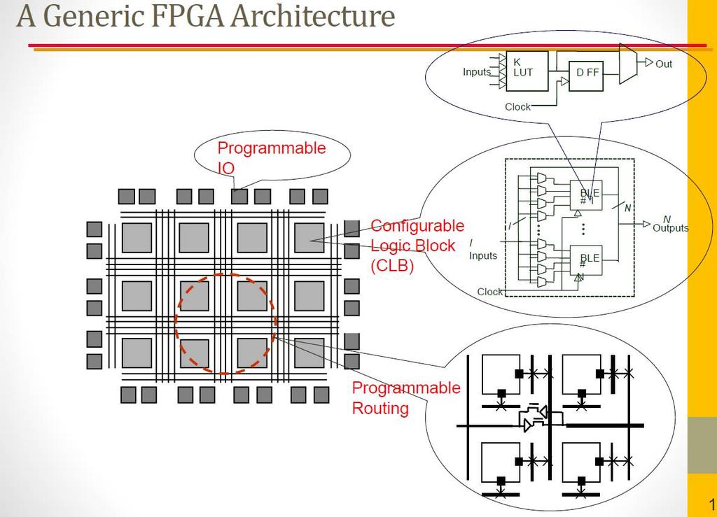
28 A simple Logic Block in FPGA Each CLB (or programmable logic block) can be programmed to perform a certain function MUX can be used to select either d or output of the LUT Flip flop can be triggered either for L-H or H-L transition

29 Configuring a LUT
30 An Implementation of a LUT

31 Top-down view of FPGA
32


33 FPGA Architecture simplified

34 Features and Specifications of the FPGA MUX based approaches


35 Features and Specifications of the FPGA LUT based approach and implementation
36 LUT vs. MUX If you take a group of logic gates several layers deep, then a LUT approach can be very efficient in terms of resource utilization and input-to-output delays. (In this context, deep refers to the number of logic gates between the inputs and the outputs. However, one downside to a LUT-based architecture is that if you only want to implement a small function such as a 2-input AND gate somewhere in your design, you ll end up using an entire LUT to do so. In addition to being wasteful in terms of resources, the resulting delays are high for such a simple function.
->CLB (with four slices) is that it is complemented by an equivalent hierarchy in the interconnect.")

37 Features and Specifications of the FPGA Slices formed of Logic Cells. LC->Slice (with two LCs)->CLB (with four slices) is that it is complemented by an equivalent hierarchy in the interconnect. Thus, there is fast interconnect between the LCs in a slice, then slightly slower interconnect between slices in a CLB, followed by the interconnect between CLBs. The idea is to achieve the optimum trade-off between making it easy to connect things together without incurring excessive interconnect-related delays.
 per CLB corresponds")
38 Distributed RAM s Assuming a 4-input LUT we can have a 16x1 RAM 4 slices (with each slices having two logic cells) per CLB corresponds to:
39 Fast Carry Chains Each LC is connected within each slice. Slices are connected with each other in CLB s. CLB s are also connected with carry chains. With the addition of embedded multipliers in FPGA fabric Makes it suitable for DSP applications


40 RAM Implementation A lot of apps now need RAM built into the FPGA. Depending on the device, such a RAM might be able to hold anywhere from a few thousand to tens of thousands of bits. Furthermore, a device might contain anywhere from tens to hundreds of these RAM blocks, thereby providing a total storage capacity of a few hundred thousand bits all the way up to several million bits. These may be scattered around or mostly in blocks.

41 Embedded multipliers, adders, MACs, etc. Some functions, like multipliers, are inherently slow if they are implemented by connecting a large number of programmable logic blocks together. Since these functions are required by a lot of applications, many FPGAs incorporate special hardwired multiplier blocks. These are typically located in close proximity to the embedded RAM blocks introduced in the previous point because these functions are often used in conjunction with each other

42 MAC block implementation Some FPGAs offer dedicated adder blocks. One operation that is very common in DSP-type applications is called a multiply-andaccumulate (MAC)
43 IP? An IP (intellectual property) core is a block of logic or data that is used in making a field programmable gate array ( FPGA ) or application-specific integrated circuit ( ASIC ) for a product. As essential elements of design reuse, IP cores are part of the growing electronic design automation ( EDA ) industry trend towards repeated use of previously designed components. Universal Asynchronous Receiver/Transmitter (UARTs), central processing units (CPUs), Ethernet controllers, and PCI interfaces are all examples of IP cores. IP cores fall into one of three categories: hard cores, firm cores, or soft cores. Hard cores are physical manifestations of the IP design. These are best for plug-and play applications, and are less portable and flexible than the other two types of cores. Like the hard cores, firm (sometimes called semi-hard ) cores also carry placement data but are configurable to various applications. Firm-cores are encrypted black boxes that are integrated into design flow in the same way as library elements The most flexible of the three, soft cores exist either as a netlist (a list of the logic gate s and associated interconnections making up an integrated circuit ) or hardware description language ( HDL ) code.
44 Embedded processor cores (hard and soft) an electronic design can be realized in hardware (using logic gates and registers, etc.) or software (as instructions to be executed on a microprocessor). Picosecond and nanosecond logic: This has to run insanely fast, which mandates that it be implemented in hardware (in the FPGA fabric). Microsecond logic: This is reasonably fast and can be implemented either in hardware or software (this type of logic is where you spend the bulk of your time deciding which way to go). Millisecond logic: This is the logic used to implement interfaces such as reading switch positions and flashing light-emitting diodes (LEDs). It s a pain slowing the hardware down to implement this sort of function (using huge counters to generate delays, for example). Thus, it s often better to implement these tasks as microprocessor code (because processors give you lousy speed compared to dedicated hardware but fantastic complexity).


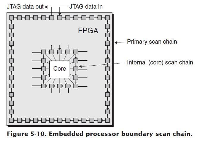
45 Embedded processor cores (hard) high-end FPGAs have become available that contain one or more embedded microprocessors, which are typically referred to as microprocessor cores. A hard microprocessor core is implemented as a dedicated, predefined block. There are two main approaches for integrating such a core into the FPGA. The first is to locate it in a strip (actually called The Stripe ) to the side of the main FPGA fabric
46 Embedded processor cores (hard) Hard IP cores ROM, RAM, FIFO RISC CPU DSP Multiplier Flash memory (boot, user) PCI, PCIe JTAG

")
47 Embedded processor cores (hard)


48 Embedded processor cores (soft) As opposed to embedding a microprocessor physically into the fabric of the chip, it is possible to configure a group of programmable logic blocks to act as a microprocessor. Soft cores are simpler (more primitive) and slower than their hard-core counterparts.2 However, they have the advantage that you only need to implement a core if you need it and also that you can instantiate as many cores as you require until you run out of resources in the form of programmable logic blocks.
49 Embedded processor cores (soft) PCI master-target, 32/64 bit, PCIe Ethernet, UART μp, μc (incl. old ones), RISC CPUs Interface to DRAM, SSRAM DSP: CORDIC, DDS, FFT, Filters VME, USB, CAN, I2C, SPI, SD card encryption / decryption
50 Sources of IP 1. Internally created blocks from previous designs, 2. FPGA vendors, 3. Third-party IP providers.
51 Handcrafted IP One scenario is that the IP provider has handcrafted an IP block starting with an RTL description also have used an IP block/core generator application In this case, there are several ways in which the end user might purchase and use such a block
52 IP at the unencrypted RTL level In certain cases, FPGA designers can purchase IP at the RTL level as blocks of unencrypted source code. These blocks can then be integrated into the RTL code for the body of the design (a). These are already simulated, synthesized, and verified the IP blocks before handing over the RTL source code). This is an expensive option because IP providers typically don t want anyone to see their RTL source code. The IP provider may charge you an arm and a leg, and you ll end up signing all sorts of licensing and nondisclosure agreements (NDAs)
53 IP at the unplaced-and-unrouted netlist level Perhaps the most common scenario is for FPGA designers to purchase IP at the unplaced-and-unrouted LUT/CLB netlist level (b) Such netlists are typically provided in encrypted form, either as encrypted EDIF or using some FPGA vendor-specific format One disadvantage is that the FPGA designer doesn t have any ability to remove unwanted functionality. Another disadvantage is that the IP block is tied to a particular FPGA vendor and device family.
54 IP at the placed-and-routed netlist level In certain cases, the FPGA designer may purchase IP at the placed-and-routed LUT/CLB netlist level Such netlists are typically provided in encrypted form, either as encrypted EDIF or using some FPGA vendor-specific format The reason for having placed-and-routed representations is to obtain the highest levels of performance. In some cases the placements will be relative, which means that the locations of all of the LUT, CLB, and other elements forming the block are fixed with respect to each other, but the block as a whole may be positioned anywhere (suitable) within the FPGA.
55 IP core generators Another very common practice is for FPGA vendors (sometimes EDA vendors, IP providers, and even small, independent design houses) to provide special tools that act as IP block/core generators. These generator applications are parameterized, thereby allows to specify the widths and depths, or both of buses and functional elements. First, you get to select from a list of different blocks/cores, and then you get to specify the parameters to be associated with each. In the case of some blocks/cores, the generator application may allow you to select from a list of functional elements that you wish to be included or excluded from the final representation. In the case of a communications block, for example, it might be possible to include or exclude certain error-checking logic. Or in the case of a CPU core, it might be possible to omit certain instructions or addressing modes. This allows the generator application to create the most efficient IP block/core in terms of its resource requirements and performance.

56 IP core generators Depending on the origin of the generator application (or sometimes the licensing option you ve signed up for), its output may be in the form of encrypted or unencrypted RTL source code, an unplaced-and-unrouted netlist, or a placedand- routed netlist.

57 Clock trees and clock managers All of the synchronous elements inside an FPGA for example, the registers configured to act as flipflops inside the programmable logic blocks need to be driven by a clock signal. Such a clock signal typically originates in the outside world, comes into the FPGA via a special clock input pin, and is then routed through the device and connected to the appropriate registers. This is called a clock tree because the main clock signal branches again and again (the flip-flops can be consider, to be the leaves on the end of the branches). This structure is used to ensure that all of the flip-flops see their versions of the clock signal as close together as possible. If the clock were distributed as a single long track driving all of the flip-flops one after another, then the flip-flop closest to the clock pin would see the clock signal much sooner than the one at the end of the chain. This is referred to as skew, and it can cause all sorts of problems

58 Clock managers Phase shifting Auto-skew correction: Jitter removal Freq. Synthesis

59 General-purpose I/O Each bank can be configured individually to support a particular I/O standard. In addition to allowing the FPGA to work with devices using multiple I/O standards, this allows the FPGA to actually be used to interface between different I/O standards today s FPGAs allow the use of internal terminating resistors whose values can be configured by the user to accommodate different circuit board environments and I/O standards. different I/O standards may use signals with voltage levels significantly different from the core voltage, so each bank of generalpurpose I/Os can have its own additional supply pins.

60 Communication with the FPGA

61 Gigabit transceivers
62 Programming an FPGA configuration file (sometimes called a bit file), which contains the information that will be uploaded into the FPGA in order to program it to perform a specific fun In the case of SRAM-based FPGAs, the configuration file contains a mixture of configuration data (bits that are used to define the state of programmable logic elements directly) and configuration commands (instructions that tell the device what to do with the configuration data). When the configuration file is in the process of being loaded into the device, the information being transferred is referred to as the configuration bitstream.
.")
63 Programming an FPGA The underlying concept associated with programming an FPGA is relatively simple (i.e., load the configuration file into the device).
, and they always need to be reprogrammed when power is first applied to the")
64 Programming an FPGA these devices are volatile, which means that they have to be programmed in-system (on the circuit board), and they always need to be reprogrammed when power is first applied to the system.

65 Programming an FPGA From the outside world, we can visualize all of the SRAM configuration cells as comprising a single (long) shift register. Consider a simple bird s-eye view of the surface of the chip showing only the I/O pins/pads and the SRAM configuration cells

66 Programming an FPGA The problem is that an FPGA can contain a humongous number of configuration cells. By 2003, for example, a reasonably high-end device could easily contain 25 million such cells! The core of a flip-flop requires eight transistors, while the core of a latch requires only four transistors. For this reason, the configuration cells in an SRAM-based FPGA are formed from latches.

67 Programming an FPGA

68 Programming an FPGA


69 Programming an FPGA

70 Programming an FPGA

71 Programming an FPGA
72 Programming an FPGA
73 Who are the players?

74
75 Age of an FPGA 1 human year = 15 years in FPGA years
Hardware Design with VHDL PLDs IV ECE 443
 Embedded Processor Cores (Hard and Soft) Electronic design can be realized in hardware (logic gates/registers) or software (instructions executed on a microprocessor). The trade-off is determined by how
Programmable Logic Devices FPGA Architectures II CMPE 415. Overview This set of notes introduces many of the features available in the FPGAs of today.
 Overview This set of notes introduces many of the features available in the FPGAs of today. The majority use SRAM based configuration cells, which allows fast reconfiguation. Allows new design ideas to
FPGA for Complex System Implementation. National Chiao Tung University Chun-Jen Tsai 04/14/2011
 FPGA for Complex System Implementation National Chiao Tung University Chun-Jen Tsai 04/14/2011 About FPGA FPGA was invented by Ross Freeman in 1989 SRAM-based FPGA properties Standard parts Allowing multi-level
Chapter 5: ASICs Vs. PLDs
 Chapter 5: ASICs Vs. PLDs 5.1 Introduction A general definition of the term Application Specific Integrated Circuit (ASIC) is virtually every type of chip that is designed to perform a dedicated task.
L2: FPGA HARDWARE : ADVANCED DIGITAL DESIGN PROJECT FALL 2015 BRANDON LUCIA
 L2: FPGA HARDWARE 18-545: ADVANCED DIGITAL DESIGN PROJECT FALL 2015 BRANDON LUCIA 18-545: FALL 2014 2 Admin stuff Project Proposals happen on Monday Be prepared to give an in-class presentation Lab 1 is
Digital Integrated Circuits
 Digital Integrated Circuits Lecture 9 Jaeyong Chung Robust Systems Laboratory Incheon National University DIGITAL DESIGN FLOW Chung EPC6055 2 FPGA vs. ASIC FPGA (A programmable Logic Device) Faster time-to-market
Basic FPGA Architectures. Actel FPGAs. PLD Technologies: Antifuse. 3 Digital Systems Implementation Programmable Logic Devices
 3 Digital Systems Implementation Programmable Logic Devices Basic FPGA Architectures Why Programmable Logic Devices (PLDs)? Low cost, low risk way of implementing digital circuits as application specific
EECS150 - Digital Design Lecture 6 - Field Programmable Gate Arrays (FPGAs)
") EECS150 - Digital Design Lecture 6 - Field Programmable Gate Arrays (FPGAs) September 12, 2002 John Wawrzynek Fall 2002 EECS150 - Lec06-FPGA Page 1 Outline What are FPGAs? Why use FPGAs (a short history
EECS150 - Digital Design Lecture 6 - Field Programmable Gate Arrays (FPGAs) September 12, 2002 John Wawrzynek Fall 2002 EECS150 - Lec06-FPGA Page 1 Outline What are FPGAs? Why use FPGAs (a short history
Outline. EECS150 - Digital Design Lecture 6 - Field Programmable Gate Arrays (FPGAs) FPGA Overview. Why FPGAs?
 FPGA Overview. Why FPGAs?") EECS150 - Digital Design Lecture 6 - Field Programmable Gate Arrays (FPGAs) September 12, 2002 John Wawrzynek Outline What are FPGAs? Why use FPGAs (a short history lesson). FPGA variations Internal logic
EECS150 - Digital Design Lecture 6 - Field Programmable Gate Arrays (FPGAs) September 12, 2002 John Wawrzynek Outline What are FPGAs? Why use FPGAs (a short history lesson). FPGA variations Internal logic
Introduction to VHDL Design on Quartus II and DE2 Board
 ECP3116 Digital Computer Design Lab Experiment Duration: 3 hours Introduction to VHDL Design on Quartus II and DE2 Board Objective To learn how to create projects using Quartus II, design circuits and
Field Program mable Gate Arrays
 Field Program mable Gate Arrays M andakini Patil E H E P g r o u p D H E P T I F R SERC school NISER, Bhubaneshwar Nov 7-27 2017 Outline Digital electronics Short history of programmable logic devices
EITF35: Introduction to Structured VLSI Design
 EITF35: Introduction to Structured VLSI Design Introduction to FPGA design Rakesh Gangarajaiah Rakesh.gangarajaiah@eit.lth.se Slides from Chenxin Zhang and Steffan Malkowsky WWW.FPGA What is FPGA? Field
CMPE 415 Programmable Logic Devices FPGA Technology I
 Department of Computer Science and Electrical Engineering CMPE 415 Programmable Logic Devices FPGA Technology I Prof. Ryan Robucci Some slides (blue-frame) developed by Jim Plusquellic Some images credited
Today. Comments about assignment Max 1/T (skew = 0) Max clock skew? Comments about assignment 3 ASICs and Programmable logic Others courses
 Max clock skew? Comments about assignment 3 ASICs and Programmable logic Others courses") Today Comments about assignment 3-43 Comments about assignment 3 ASICs and Programmable logic Others courses octor Per should show up in the end of the lecture Mealy machines can not be coded in a single
Today Comments about assignment 3-43 Comments about assignment 3 ASICs and Programmable logic Others courses octor Per should show up in the end of the lecture Mealy machines can not be coded in a single
Introduction to Field Programmable Gate Arrays
 Introduction to Field Programmable Gate Arrays Lecture 1/3 CERN Accelerator School on Digital Signal Processing Sigtuna, Sweden, 31 May 9 June 2007 Javier Serrano, CERN AB-CO-HT Outline Historical introduction.
PLAs & PALs. Programmable Logic Devices (PLDs) PLAs and PALs
 PLAs and PALs") PLAs & PALs Programmable Logic Devices (PLDs) PLAs and PALs PLAs&PALs By the late 1970s, standard logic devices were all the rage, and printed circuit boards were loaded with them. To offer the ultimate
PLAs & PALs Programmable Logic Devices (PLDs) PLAs and PALs PLAs&PALs By the late 1970s, standard logic devices were all the rage, and printed circuit boards were loaded with them. To offer the ultimate
Programmable Logic Devices Introduction CMPE 415. Programmable Logic Devices
 Instructor: Professor Jim Plusquellic Programmable Logic Devices Text: The Design Warrior s Guide to FPGAs, Devices, Tools and Flows, Clive "Max" Maxfield, ISBN: 0-7506-7604-3 Modeling, Synthesis and Rapid
Field Programmable Gate Array (FPGA)
") Field Programmable Gate Array (FPGA) Lecturer: Krébesz, Tamas 1 FPGA in general Reprogrammable Si chip Invented in 1985 by Ross Freeman (Xilinx inc.) Combines the advantages of ASIC and uc-based systems
Field Programmable Gate Array (FPGA) Lecturer: Krébesz, Tamas 1 FPGA in general Reprogrammable Si chip Invented in 1985 by Ross Freeman (Xilinx inc.) Combines the advantages of ASIC and uc-based systems
Programmable Logic Devices
 Programmable Logic Devices INTRODUCTION A programmable logic device or PLD is an electronic component used to build reconfigurable digital circuits. Unlike a logic gate, which has a fixed function, a PLD
EN2911X: Reconfigurable Computing Lecture 01: Introduction
 EN2911X: Reconfigurable Computing Lecture 01: Introduction Prof. Sherief Reda Division of Engineering, Brown University Fall 2009 Methods for executing computations Hardware (Application Specific Integrated
FPGA: What? Why? Marco D. Santambrogio
 FPGA: What? Why? Marco D. Santambrogio marco.santambrogio@polimi.it 2 Reconfigurable Hardware Reconfigurable computing is intended to fill the gap between hardware and software, achieving potentially much
FPGA Based Digital Design Using Verilog HDL
 FPGA Based Digital Design Using Course Designed by: IRFAN FAISAL MIR ( Verilog / FPGA Designer ) irfanfaisalmir@yahoo.com * Organized by Electronics Division Integrated Circuits Uses for digital IC technology
An Introduction to Programmable Logic
 Outline An Introduction to Programmable Logic 3 November 24 Transistors Logic Gates CPLD Architectures FPGA Architectures Device Considerations Soft Core Processors Design Example Quiz Semiconductors Semiconductor
INTRODUCTION TO FPGA ARCHITECTURE
 3/3/25 INTRODUCTION TO FPGA ARCHITECTURE DIGITAL LOGIC DESIGN (BASIC TECHNIQUES) a b a y 2input Black Box y b Functional Schematic a b y a b y a b y 2 Truth Table (AND) Truth Table (OR) Truth Table (XOR)
FPGA How do they work?
 ent FPGA How do they work? ETI135, Advanced Digital IC Design What is a FPGA? Manufacturers Distributed RAM History FPGA vs ASIC FPGA and Microprocessors Alternatives to FPGAs Anders Skoog, Stefan Granlund
CS310 Embedded Computer Systems. Maeng
 1 INTRODUCTION (PART II) Maeng Three key embedded system technologies 2 Technology A manner of accomplishing a task, especially using technical processes, methods, or knowledge Three key technologies for
discrete logic do not
 Welcome to my second year course on Digital Electronics. You will find that the slides are supported by notes embedded with the Powerpoint presentations. All my teaching materials are also available on
Advanced Digital Design Using FPGA. Dr. Shahrokh Abadi
 Advanced Digital Design Using FPGA Dr. Shahrokh Abadi 1 Venue Computer Lab: Tuesdays 10 12 am (Fixed) Computer Lab: Wednesday 10-12 am (Every other odd weeks) Note: Due to some unpredicted problems with
Digital Electronics 27. Digital System Design using PLDs
 1 Module -27 Digital System Design 1. Introduction 2. Digital System Design 2.1 Standard (Fixed function) ICs based approach 2.2 Programmable ICs based approach 3. Comparison of Digital System Design approaches
Evolution of Implementation Technologies. ECE 4211/5211 Rapid Prototyping with FPGAs. Gate Array Technology (IBM s) Programmable Logic
 Programmable Logic") ECE 42/52 Rapid Prototyping with FPGAs Dr. Charlie Wang Department of Electrical and Computer Engineering University of Colorado at Colorado Springs Evolution of Implementation Technologies Discrete devices:
ECE 42/52 Rapid Prototyping with FPGAs Dr. Charlie Wang Department of Electrical and Computer Engineering University of Colorado at Colorado Springs Evolution of Implementation Technologies Discrete devices:
ECEN 449 Microprocessor System Design. FPGAs and Reconfigurable Computing
 ECEN 449 Microprocessor System Design FPGAs and Reconfigurable Computing Some of the notes for this course were developed using the course notes for ECE 412 from the University of Illinois, Urbana-Champaign
Hardware Design with VHDL PLDs I ECE 443. FPGAs can be configured at least once, many are reprogrammable.
 PLDs, ASICs and FPGAs FPGA definition: Digital integrated circuit that contains configurable blocks of logic and configurable interconnects between these blocks. Key points: Manufacturer does NOT determine
Workspace for '4-FPGA' Page 1 (row 1, column 1)
") Workspace for '4-FPGA' Page 1 (row 1, column 1) Workspace for '4-FPGA' Page 2 (row 2, column 1) Workspace for '4-FPGA' Page 3 (row 3, column 1) ECEN 449 Microprocessor System Design FPGAs and Reconfigurable
Workspace for '4-FPGA' Page 1 (row 1, column 1) Workspace for '4-FPGA' Page 2 (row 2, column 1) Workspace for '4-FPGA' Page 3 (row 3, column 1) ECEN 449 Microprocessor System Design FPGAs and Reconfigurable
ECE 448 Lecture 15. Overview of Embedded SoC Systems
 ECE 448 Lecture 15 Overview of Embedded SoC Systems ECE 448 FPGA and ASIC Design with VHDL George Mason University Required Reading P. Chu, FPGA Prototyping by VHDL Examples Chapter 8, Overview of Embedded
FPGA. Logic Block. Plessey FPGA: basic building block here is 2-input NAND gate which is connected to each other to implement desired function.
 FPGA Logic block of an FPGA can be configured in such a way that it can provide functionality as simple as that of transistor or as complex as that of a microprocessor. It can used to implement different
CMPE 415 Programmable Logic Devices Introduction
 Department of Computer Science and Electrical Engineering CMPE 415 Programmable Logic Devices Introduction Prof. Ryan Robucci What are FPGAs? Field programmable Gate Array Typically re programmable as
System-on Solution from Altera and Xilinx
 System-on on-a-programmable-chip Solution from Altera and Xilinx Xun Yang VLSI CAD Lab, Computer Science Department, UCLA FPGAs with Embedded Microprocessors Combination of embedded processors and programmable
Design Methodologies. Full-Custom Design
 Design Methodologies Design styles Full-custom design Standard-cell design Programmable logic Gate arrays and field-programmable gate arrays (FPGAs) Sea of gates System-on-a-chip (embedded cores) Design
Intelop. *As new IP blocks become available, please contact the factory for the latest updated info.
 A FPGA based development platform as part of an EDK is available to target intelop provided IPs or other standard IPs. The platform with Virtex-4 FX12 Evaluation Kit provides a complete hardware environment
Xilinx DSP. High Performance Signal Processing. January 1998
 DSP High Performance Signal Processing January 1998 New High Performance DSP Alternative New advantages in FPGA technology and tools: DSP offers a new alternative to ASICs, fixed function DSP devices,
FPGA for Software Engineers
 FPGA for Software Engineers Course Description This course closes the gap between hardware and software engineers by providing the software engineer all the necessary FPGA concepts and terms. The course
EN2911X: Reconfigurable Computing Topic 01: Programmable Logic
 EN2911X: Reconfigurable Computing Topic 01: Programmable Logic Prof. Sherief Reda School of Engineering, Brown University Fall 2012 1 FPGA architecture Programmable interconnect Programmable logic blocks
Design Methodologies and Tools. Full-Custom Design
 Design Methodologies and Tools Design styles Full-custom design Standard-cell design Programmable logic Gate arrays and field-programmable gate arrays (FPGAs) Sea of gates System-on-a-chip (embedded cores)
FPGA architecture and design technology
 CE 435 Embedded Systems Spring 2017 FPGA architecture and design technology Nikos Bellas Computer and Communications Engineering Department University of Thessaly 1 FPGA fabric A generic island-style FPGA
Memory and Programmable Logic
 Digital Circuit Design and Language Memory and Programmable Logic Chang, Ik Joon Kyunghee University Memory Classification based on functionality ROM : Read-Only Memory RWM : Read-Write Memory RWM NVRWM
Spiral 2-8. Cell Layout
 2-8.1 Spiral 2-8 Cell Layout 2-8.2 Learning Outcomes I understand how a digital circuit is composed of layers of materials forming transistors and wires I understand how each layer is expressed as geometric
Overview. CSE372 Digital Systems Organization and Design Lab. Hardware CAD. Two Types of Chips
 Overview CSE372 Digital Systems Organization and Design Lab Prof. Milo Martin Unit 5: Hardware Synthesis CAD (Computer Aided Design) Use computers to design computers Virtuous cycle Architectural-level,
EECS150 - Digital Design Lecture 16 - Memory
 EECS150 - Digital Design Lecture 16 - Memory October 17, 2002 John Wawrzynek Fall 2002 EECS150 - Lec16-mem1 Page 1 Memory Basics Uses: data & program storage general purpose registers buffering table lookups
Advanced course on Embedded Systems design using FPGA
 Advanced course on Embedded Systems design using FPGA Subramaniam Ganesan, Phares A. Noel, Ashok Prajapati Oakland University, ganesan@oakland.edu, panoel@oakland.edu, akprajap@oakland.edu Abstract-As
Very Large Scale Integration (VLSI)
") Very Large Scale Integration (VLSI) Lecture 6 Dr. Ahmed H. Madian Ah_madian@hotmail.com Dr. Ahmed H. Madian-VLSI 1 Contents FPGA Technology Programmable logic Cell (PLC) Mux-based cells Look up table PLA
Very Large Scale Integration (VLSI) Lecture 6 Dr. Ahmed H. Madian Ah_madian@hotmail.com Dr. Ahmed H. Madian-VLSI 1 Contents FPGA Technology Programmable logic Cell (PLC) Mux-based cells Look up table PLA
Digital Systems Design. System on a Programmable Chip
 Digital Systems Design Introduction to System on a Programmable Chip Dr. D. J. Jackson Lecture 11-1 System on a Programmable Chip Generally involves utilization of a large FPGA Large number of logic elements
INTRODUCTION TO FIELD PROGRAMMABLE GATE ARRAYS (FPGAS)
") INTRODUCTION TO FIELD PROGRAMMABLE GATE ARRAYS (FPGAS) Bill Jason P. Tomas Dept. of Electrical and Computer Engineering University of Nevada Las Vegas FIELD PROGRAMMABLE ARRAYS Dominant digital design
INTRODUCTION TO FIELD PROGRAMMABLE GATE ARRAYS (FPGAS) Bill Jason P. Tomas Dept. of Electrical and Computer Engineering University of Nevada Las Vegas FIELD PROGRAMMABLE ARRAYS Dominant digital design
Hardware Design Environments. Dr. Mahdi Abbasi Computer Engineering Department Bu-Ali Sina University
 Hardware Design Environments Dr. Mahdi Abbasi Computer Engineering Department Bu-Ali Sina University Outline Welcome to COE 405 Digital System Design Design Domains and Levels of Abstractions Synthesis
The QR code here provides a shortcut to go to the course webpage.
 Welcome to this MSc Lab Experiment. All my teaching materials for this Lab-based module are also available on the webpage: www.ee.ic.ac.uk/pcheung/teaching/msc_experiment/ The QR code here provides a shortcut
Summer 2003 Lecture 18 07/09/03
 Summer 2003 Lecture 18 07/09/03 NEW HOMEWORK Instruction Execution Times: The 8088 CPU is a synchronous machine that operates at a particular clock frequency. In the case of the original IBM PC, that clock
FPGA Implementations
 FPGA Implementations Smith Text: Chapters 4-8 Online version at: http://www10.edacafe.com/book/asic/asics.php Topic outline Chapter 4 Programmable ASIC technologies Chapter 5 Programmable logic cells Chapter
The Xilinx XC6200 chip, the software tools and the board development tools
 The Xilinx XC6200 chip, the software tools and the board development tools What is an FPGA? Field Programmable Gate Array Fully programmable alternative to a customized chip Used to implement functions
NIOS CPU Based Embedded Computer System on Programmable Chip
 NIOS CPU Based Embedded Computer System on Programmable Chip 1 Lab Objectives EE8205: Embedded Computer Systems NIOS-II SoPC: PART-I This lab has been constructed to introduce the development of dedicated
DIGITAL DESIGN TECHNOLOGY & TECHNIQUES
 DIGITAL DESIGN TECHNOLOGY & TECHNIQUES CAD for ASIC Design 1 INTEGRATED CIRCUITS (IC) An integrated circuit (IC) consists complex electronic circuitries and their interconnections. William Shockley et
Zynq-7000 All Programmable SoC Product Overview
 Zynq-7000 All Programmable SoC Product Overview The SW, HW and IO Programmable Platform August 2012 Copyright 2012 2009 Xilinx Introducing the Zynq -7000 All Programmable SoC Breakthrough Processing Platform
Spartan-3E FPGA Design Guide for prototyping and production environment
 3ème conférence Internationale des énergies renouvelables CIER-2015 Proceedings of Engineering and Technology - PET Spartan-3E FPGA Design Guide for prototyping and production environment Mohammed BOUDJEMA
Programmable Logic Devices UNIT II DIGITAL SYSTEM DESIGN
 Programmable Logic Devices UNIT II DIGITAL SYSTEM DESIGN 2 3 4 5 6 7 8 9 2 3 4 5 6 7 8 9 2 Implementation in Sequential Logic 2 PAL Logic Implementation Design Example: BCD to Gray Code Converter A B
Memory and Programmable Logic
 Memory and Programmable Logic Memory units allow us to store and/or retrieve information Essentially look-up tables Good for storing data, not for function implementation Programmable logic device (PLD),
ECE 353 Lab 4. MIDI Receiver in Verilog. Professor Daniel Holcomb UMass Amherst Fall 2016
 ECE 353 Lab 4 MIDI Receiver in Verilog Professor Daniel Holcomb UMass Amherst Fall 2016 Timeline and Grading for Lab 4 Lectures on 11/15 and 11/17 Due on 12/12 Demos in Duda hall Schedule will be posted
EMBEDDED SOPC DESIGN WITH NIOS II PROCESSOR AND VHDL EXAMPLES
 EMBEDDED SOPC DESIGN WITH NIOS II PROCESSOR AND VHDL EXAMPLES Pong P. Chu Cleveland State University A JOHN WILEY & SONS, INC., PUBLICATION PREFACE An SoC (system on a chip) integrates a processor, memory
Embedded Systems: Hardware Components (part I) Todor Stefanov
 Todor Stefanov") Embedded Systems: Hardware Components (part I) Todor Stefanov Leiden Embedded Research Center Leiden Institute of Advanced Computer Science Leiden University, The Netherlands Outline Generic Embedded System
Embedded Systems: Hardware Components (part I) Todor Stefanov Leiden Embedded Research Center Leiden Institute of Advanced Computer Science Leiden University, The Netherlands Outline Generic Embedded System
Overview of Microcontroller and Embedded Systems
 UNIT-III Overview of Microcontroller and Embedded Systems Embedded Hardware and Various Building Blocks: The basic hardware components of an embedded system shown in a block diagram in below figure. These
Graduate Institute of Electronics Engineering, NTU Advanced VLSI SOPC design flow
 Advanced VLSI SOPC design flow Advisor: Speaker: ACCESS IC LAB What s SOC? IP classification IP reusable & benefit Outline SOPC solution on FPGA SOPC design flow pp. 2 What s SOC? Definition of SOC Advantage
Lecture 7. Standard ICs FPGA (Field Programmable Gate Array) VHDL (Very-high-speed integrated circuits. Hardware Description Language)
 VHDL (Very-high-speed integrated circuits. Hardware Description Language)") Standard ICs FPGA (Field Programmable Gate Array) VHDL (Very-high-speed integrated circuits Hardware Description Language) 1 Standard ICs PLD: Programmable Logic Device CPLD: Complex PLD FPGA: Field Programmable
Standard ICs FPGA (Field Programmable Gate Array) VHDL (Very-high-speed integrated circuits Hardware Description Language) 1 Standard ICs PLD: Programmable Logic Device CPLD: Complex PLD FPGA: Field Programmable
NIOS CPU Based Embedded Computer System on Programmable Chip
 1 Objectives NIOS CPU Based Embedded Computer System on Programmable Chip EE8205: Embedded Computer Systems This lab has been constructed to introduce the development of dedicated embedded system based
Organization. 5.1 Semiconductor Main Memory. William Stallings Computer Organization and Architecture 6th Edition
 William Stallings Computer Organization and Architecture 6th Edition Chapter 5 Internal Memory 5.1 Semiconductor Main Memory 5.2 Error Correction 5.3 Advanced DRAM Organization 5.1 Semiconductor Main Memory
9. Building Memory Subsystems Using SOPC Builder
 9. Building Memory Subsystems Using SOPC Builder QII54006-6.0.0 Introduction Most systems generated with SOPC Builder require memory. For example, embedded processor systems require memory for software
FPGA for Dummies. Introduc)on to Programmable Logic
on to Programmable Logic") FPGA for Dummies Introduc)on to Programmable Logic FPGA for Dummies Historical introduc)on, where we come from; FPGA Architecture: Ø basic blocks (Logic, FFs, wires and IOs); Ø addi)onal elements; FPGA
FPGA for Dummies Introduc)on to Programmable Logic FPGA for Dummies Historical introduc)on, where we come from; FPGA Architecture: Ø basic blocks (Logic, FFs, wires and IOs); Ø addi)onal elements; FPGA
Chapter 13 Programmable Logic Device Architectures
 Chapter 13 Programmable Logic Device Architectures Chapter 13 Objectives Selected areas covered in this chapter: Describing different categories of digital system devices. Describing different types of
Computer Structure. Unit 2: Memory and programmable devices
 Computer Structure Unit 2: Memory and programmable devices Translated from Francisco Pérez García (fperez at us.es) by Mª Carmen Romero (mcromerot at us.es, Office G1.51, 954554324) Electronic Technology
Programmable Logic. Any other approaches?
 Programmable Logic So far, have only talked about PALs (see 22V10 figure next page). What is the next step in the evolution of PLDs? More gates! How do we get more gates? We could put several PALs on one
Chapter 1 Overview of Digital Systems Design
 Chapter 1 Overview of Digital Systems Design SKEE2263 Digital Systems Mun im/ismahani/izam {munim@utm.my,e-izam@utm.my,ismahani@fke.utm.my} February 8, 2017 Why Digital Design? Many times, microcontrollers
PRELAB! Read the entire lab, and complete the prelab questions (Q1- Q3) on the answer sheet before coming to the laboratory.
 on the answer sheet before coming to the laboratory.") PRELAB! Read the entire lab, and complete the prelab questions (Q1- Q3) on the answer sheet before coming to the laboratory. 1.0 Objectives In this lab you will get familiar with the concept of using the
PRELAB! Read the entire lab, and complete the prelab questions (Q1- Q3) on the answer sheet before coming to the laboratory. 1.0 Objectives In this lab you will get familiar with the concept of using the
ECE 636. Reconfigurable Computing. Lecture 2. Field Programmable Gate Arrays I
 ECE 636 Reconfigurable Computing Lecture 2 Field Programmable Gate Arrays I Overview Anti-fuse and EEPROM-based devices Contemporary SRAM devices - Wiring - Embedded New trends - Single-driver wiring -
EECS150 - Digital Design Lecture 16 Memory 1
 EECS150 - Digital Design Lecture 16 Memory 1 March 13, 2003 John Wawrzynek Spring 2003 EECS150 - Lec16-mem1 Page 1 Memory Basics Uses: Whenever a large collection of state elements is required. data &
Synthesis of VHDL Code for FPGA Design Flow Using Xilinx PlanAhead Tool
 Synthesis of VHDL Code for FPGA Design Flow Using Xilinx PlanAhead Tool Md. Abdul Latif Sarker, Moon Ho Lee Division of Electronics & Information Engineering Chonbuk National University 664-14 1GA Dekjin-Dong
DIGITAL SYSTEM FUNDAMENTALS (ECE421) DIGITAL ELECTRONICS FUNDAMENTAL (ECE4220. PROGRAMMABLE LOGIC DEVICES (PLDs)
 DIGITAL ELECTRONICS FUNDAMENTAL (ECE4220. PROGRAMMABLE LOGIC DEVICES (PLDs)") COURSE / CODE DIGITAL SYSTEM FUNDAMENTALS (ECE421) DIGITAL ELECTRONICS FUNDAMENTAL (ECE4220 PROGRAMMABLE LOGIC DEVICES (PLDs) A PLD, or programmable logic device, is an electronic component that is used
COURSE / CODE DIGITAL SYSTEM FUNDAMENTALS (ECE421) DIGITAL ELECTRONICS FUNDAMENTAL (ECE4220 PROGRAMMABLE LOGIC DEVICES (PLDs) A PLD, or programmable logic device, is an electronic component that is used
Main Memory (RAM) Organisation
 Organisation") Main Memory (RAM) Organisation Computers employ many different types of memory (semi-conductor, magnetic disks, USB sticks, DVDs etc.) to hold data and programs. Each type has its own characteristics and
Main Memory (RAM) Organisation Computers employ many different types of memory (semi-conductor, magnetic disks, USB sticks, DVDs etc.) to hold data and programs. Each type has its own characteristics and
What is Xilinx Design Language?
 Bill Jason P. Tomas University of Nevada Las Vegas Dept. of Electrical and Computer Engineering What is Xilinx Design Language? XDL is a human readable ASCII format compatible with the more widely used
The Memory Component
 The Computer Memory Chapter 6 forms the first of a two chapter sequence on computer memory. Topics for this chapter include. 1. A functional description of primary computer memory, sometimes called by
Embedded Systems: Architecture
 Embedded Systems: Architecture Jinkyu Jeong (Jinkyu@skku.edu) Computer Systems Laboratory Sungkyunkwan University http://csl.skku.edu ICE3028: Embedded Systems Design, Fall 2018, Jinkyu Jeong (jinkyu@skku.edu)
S2C K7 Prodigy Logic Module Series
 S2C K7 Prodigy Logic Module Series Low-Cost Fifth Generation Rapid FPGA-based Prototyping Hardware The S2C K7 Prodigy Logic Module is equipped with one Xilinx Kintex-7 XC7K410T or XC7K325T FPGA device
Outline. Field Programmable Gate Arrays. Programming Technologies Architectures. Programming Interfaces. Historical perspective
 Outline Field Programmable Gate Arrays Historical perspective Programming Technologies Architectures PALs, PLDs,, and CPLDs FPGAs Programmable logic Interconnect network I/O buffers Specialized cores Programming
Computers Are Your Future
 Computers Are Your Future 2008 Prentice-Hall, Inc. Computers Are Your Future Chapter 6 Inside the System Unit 2008 Prentice-Hall, Inc. Slide 2 What You Will Learn... Understand how computers represent
Design of DMA Controller Using VHDL
 Design of DMA Controller Using VHDL Rashmi mishra 1, Rupal chauhan 2, Garima arora 3 1, 2 Department of Electronics & Communication BE (VII SEM) Takshshila Institute of Engineering & Technology, Jabalpur,
ECE 1160/2160 Embedded Systems Design. Midterm Review. Wei Gao. ECE 1160/2160 Embedded Systems Design
 ECE 1160/2160 Embedded Systems Design Midterm Review Wei Gao ECE 1160/2160 Embedded Systems Design 1 Midterm Exam When: next Monday (10/16) 4:30-5:45pm Where: Benedum G26 15% of your final grade What about:
FPGAs: Instant Access
 FPGAs: Instant Access Clive"Max"Maxfield AMSTERDAM BOSTON HEIDELBERG LONDON NEW YORK OXFORD PARIS SAN DIEGO SAN FRANCISCO SINGAPORE SYDNEY TOKYO % ELSEVIER Newnes is an imprint of Elsevier Newnes Contents
Chapter 5 Internal Memory
 Chapter 5 Internal Memory Memory Type Category Erasure Write Mechanism Volatility Random-access memory (RAM) Read-write memory Electrically, byte-level Electrically Volatile Read-only memory (ROM) Read-only
William Stallings Computer Organization and Architecture 6th Edition. Chapter 5 Internal Memory
 William Stallings Computer Organization and Architecture 6th Edition Chapter 5 Internal Memory Semiconductor Memory Types Semiconductor Memory RAM Misnamed as all semiconductor memory is random access
UNIT 4 INTEGRATED CIRCUIT DESIGN METHODOLOGY E5163
 UNIT 4 INTEGRATED CIRCUIT DESIGN METHODOLOGY E5163 LEARNING OUTCOMES 4.1 DESIGN METHODOLOGY By the end of this unit, student should be able to: 1. Explain the design methodology for integrated circuit.
COE 561 Digital System Design & Synthesis Introduction
 1 COE 561 Digital System Design & Synthesis Introduction Dr. Aiman H. El-Maleh Computer Engineering Department King Fahd University of Petroleum & Minerals Outline Course Topics Microelectronics Design
CREATED BY M BILAL & Arslan Ahmad Shaad Visit:
 CREATED BY M BILAL & Arslan Ahmad Shaad Visit: www.techo786.wordpress.com Q1: Define microprocessor? Short Questions Chapter No 01 Fundamental Concepts Microprocessor is a program-controlled and semiconductor
VLSI Design Automation
 VLSI Design Automation IC Products Processors CPU, DSP, Controllers Memory chips RAM, ROM, EEPROM Analog Mobile communication, audio/video processing Programmable PLA, FPGA Embedded systems Used in cars,
Computer Fundamentals and Operating System Theory. By Neil Bloomberg Spring 2017
 Computer Fundamentals and Operating System Theory By Neil Bloomberg Spring 2017 INTRODUCTION This presentation will cover the fundamentals of Computer Operating Systems as a layered architecture using
The University of Reduced Instruction Set Computer (MARC)
") The University of Reduced Instruction Set Computer (MARC) Abstract We present our design of a VHDL-based, RISC processor instantiated on an FPGA for use in undergraduate electrical engineering courses
The University of Reduced Instruction Set Computer (MARC) Abstract We present our design of a VHDL-based, RISC processor instantiated on an FPGA for use in undergraduate electrical engineering courses