Computer Structure. Unit 2: Memory and programmable devices
|
|
|
- Colleen Palmer
- 5 years ago
- Views:
Transcription
1 Computer Structure Unit 2: Memory and programmable devices Translated from Francisco Pérez García (fperez at us.es) by Mª Carmen Romero (mcromerot at us.es, Office G1.51, ) Electronic Technology Department University of Seville (February 2012)
2 Content 1. Memory 1.1 Basic concepts 1.2 Semiconductor memory classification 1.3 Random Access Memory - Read Only Memory (ROM) - Read and Write Memory (RAM) - Memory expansion 1.4 Sequential access memory 2. Programable devices: Basic architecture for a FPGA. Bibliography: Floyd. Digital Fundamentals. 10th Ed. (Ch.10, Ch.11) 2
3 1. Basic concepts Computer requires to store a huge amount of binary data permanently. Systems based on microprocessor needs memory devices to store programs and data (generated during processing). In Computer Science, memory usually refers to RAM and ROM memories and storage usually refers to disks and other external devices. 3
4 PROCESSOR Basic organization of a computer ADDRESS BUS ROM RAM I/O DATA BUS 4

5 Example of using memory in a computer 5
6 Memory Hierarchy Reg. Speed and Cost Cache Main Memory (RAM and ROM) Secondary Memory (HDD) Capacity External storage 6

7 Basic memory array Each element of storage in a memory can store 1 bit and it is called cell. Memory is made up of cells matrices. Each row of that memory array is called word and represents the information that is able to be read or written in each access.

8 Bidimensional organization of a memory
9 Memory address and capacity (Address Bus) A n M 2 n xk k D (Data Bus) Memory capacity is the amount of bits that it can store: A (Address Bus) n xk. Position of a word is called address. (Data Bus) k
10 Basic operations of memory Because they are storage devices, memory has two basic operations: Write: it allows to store a word in a particular memory address. Read: it allows to retrieve a word stored in a particular memory address. To implement these operations two buses are needed: Address bus (A n-1 : A 0 ): to indicate the read/write address. Data bus (D k-1 : D 0 ): to read/write the word. R W M A n-1 : A 0 D k-1 : D 0 10
11 Writing in memory
12 Reading from memory

13 Reading from memory Memory

14 Tridimensional organization of a memory

15 Tridimensional organization of a memory
16 Content 1. Memory 1.1 Basic concepts 1.2 Semiconductor memory classification 1.3 Random Access Memory - Read Only Memory (ROM) - Read and Write Memory (RAM) - Memory expansion 1.4 Sequential access memory 2. Programable devices: Basic architecture for a FPGA. 16
17 Classification semiconductor memory Random access Only read (ROM) Read/Write (RAM) FIFO (queue) Sequential access LIFO (stack) 17
18 Content 1. Memory 1.1 Basic concepts 1.2 Semiconductor memory classification 1.3 Random Access Memory - Read Only Memory (ROM) - Read and Write Memory (RAM) - Memory expansion 1.4 Sequential access memory 2. Programable devices: Basic architecture for a FPGA. 18
19 RAM and ROM memory The two main random access semiconductor memory categories are: ROM (Read-Only Memory): they can only be read and they are nonvolatile. RAM (Random-Access Memory): they can be read and written and they are volatile. 19

20 Family of ROM memory ROM Read Only Memory Mask ROM PROM Programmable ROM EPROM Erasable PROM UV EPROM Ultraviolet EPROM EEPROM Electrically EPROM 20
21 ROM Memory One is able to store 2 m data of n bits Non volatile It is recorded during manufacturing (ROM) or in laboratory (EPROM, EEPROM ) AB: Address BUS [A m-1 :A 0 ] DB: Data BUS [Dn-1:D0] 21
22 Example: ROM 2 3 x4 (8 positions of 4 bits) CS x y z CS: Chip Selection A 2 A 1 A 0 ROM 2 3 x 4 D 3 D 2 D 1 D 0 CS A2 A1 A0 D3 D2 D1 D HI HI HI HI In each column a function is carried out (when CS=1). E.g. D 0 = S (m 0, m 3, m 4, m 5 ) = P (M 1, M 2, M 6, M 7 ) When CS disable, outputs are in HIGH IMPEDANCE (HI) 22

23 Internal organization of a ROM. E.g.: ROM 16x8 23

24 Example of use of ROM: Natural binary code to Gray converter Address Content B3 B2 B1 B0 G3 G2 G1 G0 Natural binary code 3 bits GRAY code 24
25 Example of tridimensional organization: ROM 256x4 Array (32x8)x4 bits 25


26 Example of tridimensional organization: ROM 256x4 array (32x8)x4 bits 26
27 Example of a commercial EPROM NMC27C16B 2048x8 Bit EPROM (Fairchild s) Chip Enable/ ProGramming Mode 27
28 Access time for the commercial EPROM NMC27C16B 2048x8 Bit EPROM (Fairchild s) 28

29 Access time for the commercial EPROM NMC27C16B 2048x8 Bit EPROM (Fairchild s) 29
30 Content 1. Memory 1.1 Basic concepts 1.2 Semiconductor memory classification 1.3 Random Access Memory - Read Only Memory (ROM) - Read and Write Memory (RAM) - Memory expansion 1.4 Sequential access memory 2. Programable devices: Basic architecture for a FPGA. 30
31 RAM memory ROM (Read Only Memory): Only read, non-volatile RAM (Random Access Memory): Read/write, volatile Random access 2 main types: Static (SRAM): they keep the stored data while there is power (with flip-flops) (faster). Dynamic (DRAM): they need to refresh the information periodically ( reload condensers) (cheaper).

32 RAM cells SRAM cell DRAM cell
33 Description of RAM memory It can have unidirectional data lines (separated inputs and oputputs) or bidirectional. Description of RAM 2 n x m with bidirectional data lines: Address Bus Data Bus RW M DB = 00 M M HI 01 M(AB) DB [DB in] 10 M M DB = M(AB) 11 Forbidden Read Write


34 Internal organization of RAM (32kx8) /CS /OE /WE Mode Data Bus?
35
36 Content 1. Memory 1.1 Basic concepts 1.2 Semiconductor memory classification 1.3 Random Access Memory - Read Only Memory (ROM) - Read and Write Memory (RAM) - Memory expansion (association) 1.4 Sequential access memory 2. Programable devices: Basic architecture for a FPGA. 36

37 Word length expansion in ROM memory 37
38 Word length expansion in ROM memory Get a ROM 2 3 x 8 with two ROM 2 3 x 4 CS A2 A1 A ROM 8x ROM 8x4 ROM 8x D7D6D5D4 D3D2D1D0 38

39 Word length expansion in ROM memory E.g. Get a ROM 64kx8 with two ROM 64kx4 39
40 Word length expansion in RAM memory CS WE OE A2 A1 A RAM 8x RAM 8x4 RAM 8x D7D6D5D4 D3D2D1D0 40
41 Word length expansion in RAM memory E.g. Get a RAM 1Mx8 with two RAM 1Mx4 41

42 Word amount expansion in memory 42
43 Word amount expansion in ROM memory Get a ROM 2 4 x 4 with two ROM 2 3 x 4 CS A3 A2 A1 A ROM 8x ROM 8x ROM 16x4 D3D2D1D0 43
44 Example: word amount expansion in RAM memory CS WE OE A3 A2 A1 A RAM 8x RAM 8x RAM 16x4 D3D2D1D0 44
45 Example: word amount expansion in RAM memory E.g.: Get a RAM 1Mx4 with two RAM 512K x4 45

46 FLASH memory Read/write, high capacity and non-volatile memory TYPE Non-volatile High density Cell of 1 transistor Write insystem Flash Yes Yes Yes Yes SRAM No No No Yes DRAM No Yes Yes Yes ROM Yes Yes Yes No EPROM Yes Yes Yes No EEPROM Yes No No Yes 46
47 Content 1. Memory 1.1 Basic concepts 1.2 Semiconductor memory classification 1.3 Random Access Memory - Read Only Memory (ROM) - Read and Write Memory (RAM) - Memory expansion (association) 1.4 Sequential access memory 2. Programable devices: Basic architecture for a FPGA. 47
 Incoming data last 1st Outgoing data")
48 FIFO (First In-First Out) memory (queue; cola) Incoming data last 1st Outgoing data 48
49 LIFO (Last In-First Out) memory (stack; pila) PUSH Write new data Bottom (D) Last data TOP (R0) PULL / POP Read/Extract last data First data EMPTY STACK: When none data has been written yet FULL STACK: IDLE STACK: When D elements have been written When there isn t Pull neither Push 49

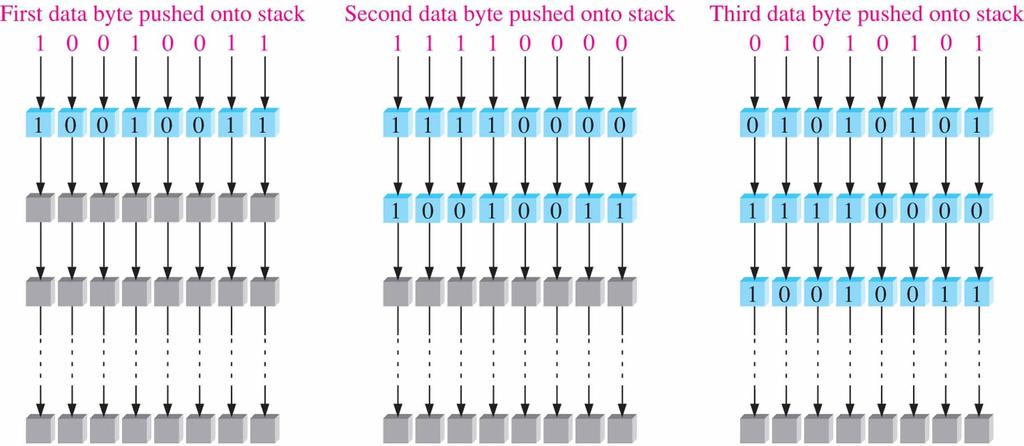
50 Writing on Stack (Pila) 50
")
51 Reading from Stack (Pila) 51
52 Content 1. Memory 1.1 Basic concepts 1.2 Semiconductor memory classification 1.3 Random Access Memory - Read Only Memory (ROM) - Read and Write Memory (RAM) - Memory expansion (association) 1.4 Sequential access memory 2. Programable devices: Basic architecture for a FPGA. 52

53 Programmable Logic Devices Designing functions with many inputs and outputs using flip-flops and gates (from K-map and state diagrams) is non-viable. PLDs: They are devices that are programmable by user to implement many functions with many variables. Large variety: SPLD (Simplex PLD): PAL/GAL, FPLA, CPLD (Complex PLD) Currently, the most used are FPGAs (Xilinx and Altera) PLD: Programmable Logic Device PAL: Programmable Array Logic GAL: Generic Array Logic FPGA: Field-Programmable Gate Array

54 Lifecycle of design with PLD PLD: Programmable Logic Device HDL: Hardware Description Language

55 Design environment with PLD
")

56 Basic structure of a PAL (SPLD) (fussel logic NON-reprogrammable) PAL: Programmable Array Logic SPLD: Simple Programmable Logic Device
 (fussel logic")

57 Product addition accomplished with a PAL (SPLD) (fussel logic NON-reprogrammable) PAL: Programmable Array Logic SPLD: Simple Programmable Logic Device

58 Basic structure of a GAL (SPLD) (It IS reprogrammable) GAL: Generic Array Logic SPLD: Simple Programmable Logic Device
")
59 Simplified notation for PAL/GAL (SPLDs)
")
60 PAL/GAL (SPLDs) architecture
61 Output logic of macrocells in PAL/GAL (SPLDs) devices


62 CPLDs (Complex PLDs) Generic architecture PLD: Programmable Logic Device SPLD: Simple Programmable Logic Device PIA: Programmable Interconnect Array

63 Example: Architecture CPLD MAX 7000 (Altera)
 A FPGA allows to")


64 FPGA (Field-Programmable Gate Array) A FPGA allows to implement any digital circuit. The only limitation is the amount of gates for the circuit. Develop is carried out using a prototype board.
65 Main manufacturers and models of FPGA Otros Others Actel Lattice Altera Market share Xilinx Xilinx: Spartan Virtex Altera: Arria Cyclone Stratix Actel: Igloo ProASIC SmartFusion

66 FPGA concept LTU: Look-Up Table

67 Basic architecture of a FPGA CLB: Configurable Logic Block

 of a")
68 Structure of Configurable Logic Blocks (CLB) of a FPGA


69 Structure of a logic module (included in CLBs) of a FPGA

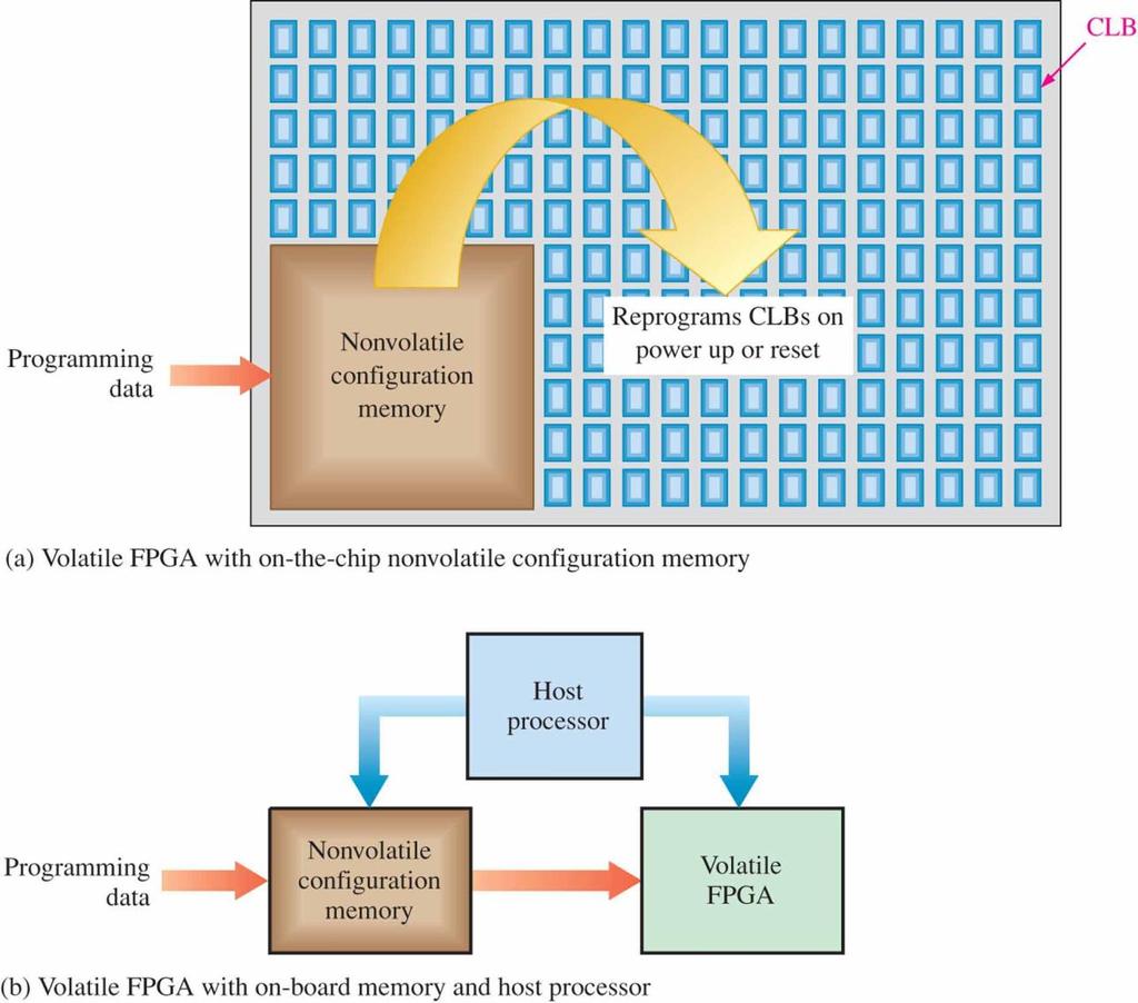
70 Examples of configurations of volatile FPGAs (LUT SRAM)

71 Advanced architectures of FPGAs DSP: Digital Signal Processor LAB: Logic Array Block

72 Advanced architectures of FPGAs Column interconnects Rows interconnects Embedded memory DSP cores I/Os CLBs (a) FPGA with fully configurable logic (b) Same size FPGA with embedded memory and DSP cores results in fewer CLBs and is limited by the perimeter I/Os. Processor core (c) FPGA with more embedded memory, additional DSP cores, and processor core will require a larger physical size at some point.
73 First projects with FPGAs
DIGITAL SYSTEM FUNDAMENTALS (ECE421) DIGITAL ELECTRONICS FUNDAMENTAL (ECE422)
 DIGITAL ELECTRONICS FUNDAMENTAL (ECE422)") COURSE / CODE DIGITAL SYSTEM FUNDAMENTALS (ECE421) DIGITAL ELECTRONICS FUNDAMENTAL (ECE422) Memory In computing, memory refers to the computer hardware devices used to store information for immediate use
COURSE / CODE DIGITAL SYSTEM FUNDAMENTALS (ECE421) DIGITAL ELECTRONICS FUNDAMENTAL (ECE422) Memory In computing, memory refers to the computer hardware devices used to store information for immediate use
ELCT 912: Advanced Embedded Systems
 Advanced Embedded Systems Lecture 2: Memory and Programmable Logic Dr. Mohamed Abd El Ghany, Memory Random Access Memory (RAM) Can be read and written Static Random Access Memory (SRAM) Data stored so
Digital Integrated Circuits
 Digital Integrated Circuits Lecture 9 Jaeyong Chung Robust Systems Laboratory Incheon National University DIGITAL DESIGN FLOW Chung EPC6055 2 FPGA vs. ASIC FPGA (A programmable Logic Device) Faster time-to-market
Memory and Programmable Logic
 Memory and Programmable Logic Mano & Ciletti Chapter 7 By Suleyman TOSUN Ankara University Outline RAM Memory decoding Error detection and correction ROM Programmable Logic Array (PLA) Programmable Array
Memory and Programmable Logic
 Digital Circuit Design and Language Memory and Programmable Logic Chang, Ik Joon Kyunghee University Memory Classification based on functionality ROM : Read-Only Memory RWM : Read-Write Memory RWM NVRWM
Chapter 13 Programmable Logic Device Architectures
 Chapter 13 Programmable Logic Device Architectures Chapter 13 Objectives Selected areas covered in this chapter: Describing different categories of digital system devices. Describing different types of
LSN 6 Programmable Logic Devices
 LSN 6 Programmable Logic Devices Department of Engineering Technology LSN 6 What Are PLDs? Functionless devices in base form Require programming to operate The logic function of the device is programmed
Programmable Logic Devices
 Programmable Logic Devices INTRODUCTION A programmable logic device or PLD is an electronic component used to build reconfigurable digital circuits. Unlike a logic gate, which has a fixed function, a PLD
Programmable Logic Devices UNIT II DIGITAL SYSTEM DESIGN
 Programmable Logic Devices UNIT II DIGITAL SYSTEM DESIGN 2 3 4 5 6 7 8 9 2 3 4 5 6 7 8 9 2 Implementation in Sequential Logic 2 PAL Logic Implementation Design Example: BCD to Gray Code Converter A B
PLAs & PALs. Programmable Logic Devices (PLDs) PLAs and PALs
 PLAs and PALs") PLAs & PALs Programmable Logic Devices (PLDs) PLAs and PALs PLAs&PALs By the late 1970s, standard logic devices were all the rage, and printed circuit boards were loaded with them. To offer the ultimate
PLAs & PALs Programmable Logic Devices (PLDs) PLAs and PALs PLAs&PALs By the late 1970s, standard logic devices were all the rage, and printed circuit boards were loaded with them. To offer the ultimate
Memory and Programmable Logic
 Memory and Programmable Logic Memory units allow us to store and/or retrieve information Essentially look-up tables Good for storing data, not for function implementation Programmable logic device (PLD),
Lecture 13: Memory and Programmable Logic
 Lecture 13: Memory and Programmable Logic Syed M. Mahmud, Ph.D ECE Department Wayne State University Aby K George, ECE Department, Wayne State University Contents Introduction Random Access Memory Memory
DIGITAL SYSTEM FUNDAMENTALS (ECE421) DIGITAL ELECTRONICS FUNDAMENTAL (ECE4220. PROGRAMMABLE LOGIC DEVICES (PLDs)
 DIGITAL ELECTRONICS FUNDAMENTAL (ECE4220. PROGRAMMABLE LOGIC DEVICES (PLDs)") COURSE / CODE DIGITAL SYSTEM FUNDAMENTALS (ECE421) DIGITAL ELECTRONICS FUNDAMENTAL (ECE4220 PROGRAMMABLE LOGIC DEVICES (PLDs) A PLD, or programmable logic device, is an electronic component that is used
COURSE / CODE DIGITAL SYSTEM FUNDAMENTALS (ECE421) DIGITAL ELECTRONICS FUNDAMENTAL (ECE4220 PROGRAMMABLE LOGIC DEVICES (PLDs) A PLD, or programmable logic device, is an electronic component that is used
Sistemas Digitais I LESI - 2º ano
 Sistemas Digitais I LESI - 2º ano Lesson 9 - Memory, CPLDs and FPGAs Prof. João Miguel Fernandes (miguel@di.uminho.pt) Dept. Informática UNIVERSIDADE DO MINHO ESCOLA DE ENGENHARIA - Memory - Any sequential
Memory Overview. Overview - Memory Types 2/17/16. Curtis Nelson Walla Walla University
 Memory Overview Curtis Nelson Walla Walla University Overview - Memory Types n n n Magnetic tape (used primarily for long term archive) Magnetic disk n Hard disk (File, Directory, Folder) n Floppy disks
UNIT V (PROGRAMMABLE LOGIC DEVICES)
") UNIT V (PROGRAMMABLE LOGIC DEVICES) Introduction There are two types of memories that are used in digital systems: Random-access memory(ram): perform both the write and read operations. Read-only memory(rom):
UNIT V (PROGRAMMABLE LOGIC DEVICES) Introduction There are two types of memories that are used in digital systems: Random-access memory(ram): perform both the write and read operations. Read-only memory(rom):
Programmable Logic Devices
 Programmable Logic Devices Luis Entrena, Celia López, Mario García, Enrique San Millán Universidad Carlos III de Madrid Outline Tecnologies for implementing programmable circuits Simple Programmable Logic
ECE 331 Digital System Design
 ECE 331 Digital System Design Tristate Buffers, Read-Only Memories and Programmable Logic Devices (Lecture #17) The slides included herein were taken from the materials accompanying Fundamentals of Logic
8051 INTERFACING TO EXTERNAL MEMORY
 8051 INTERFACING TO EXTERNAL MEMORY Memory Capacity The number of bits that a semiconductor memory chip can store Called chip capacity It can be in units of Kbits (kilobits), Mbits (megabits), and so on
Section 6. Memory Components Chapter 5.7, 5.8 Physical Implementations Chapter 7 Programmable Processors Chapter 8
 Section 6 Memory Components Chapter 5.7, 5.8 Physical Implementations Chapter 7 Programmable Processors Chapter 8 Types of memory Two major types of memory Volatile When power to the device is removed
Computer Organization and Assembly Language (CS-506)
") Computer Organization and Assembly Language (CS-506) Muhammad Zeeshan Haider Ali Lecturer ISP. Multan ali.zeeshan04@gmail.com https://zeeshanaliatisp.wordpress.com/ Lecture 2 Memory Organization and Structure
Computer Organization and Assembly Language (CS-506) Muhammad Zeeshan Haider Ali Lecturer ISP. Multan ali.zeeshan04@gmail.com https://zeeshanaliatisp.wordpress.com/ Lecture 2 Memory Organization and Structure
COMP3221: Microprocessors and. and Embedded Systems. Overview. Lecture 23: Memory Systems (I)
") COMP3221: Microprocessors and Embedded Systems Lecture 23: Memory Systems (I) Overview Memory System Hierarchy RAM, ROM, EPROM, EEPROM and FLASH http://www.cse.unsw.edu.au/~cs3221 Lecturer: Hui Wu Session
COMP3221: Microprocessors and Embedded Systems Lecture 23: Memory Systems (I) Overview Memory System Hierarchy RAM, ROM, EPROM, EEPROM and FLASH http://www.cse.unsw.edu.au/~cs3221 Lecturer: Hui Wu Session
Unit 6 1.Random Access Memory (RAM) Chapter 3 Combinational Logic Design 2.Programmable Logic
 Chapter 3 Combinational Logic Design 2.Programmable Logic") EE 200: Digital Logic Circuit Design Dr Radwan E Abdel-Aal, COE Unit 6.Random Access Memory (RAM) Chapter 3 Combinational Logic Design 2. Logic Logic and Computer Design Fundamentals Part Implementation
EE 200: Digital Logic Circuit Design Dr Radwan E Abdel-Aal, COE Unit 6.Random Access Memory (RAM) Chapter 3 Combinational Logic Design 2. Logic Logic and Computer Design Fundamentals Part Implementation
Evolution of Implementation Technologies. ECE 4211/5211 Rapid Prototyping with FPGAs. Gate Array Technology (IBM s) Programmable Logic
 Programmable Logic") ECE 42/52 Rapid Prototyping with FPGAs Dr. Charlie Wang Department of Electrical and Computer Engineering University of Colorado at Colorado Springs Evolution of Implementation Technologies Discrete devices:
ECE 42/52 Rapid Prototyping with FPGAs Dr. Charlie Wang Department of Electrical and Computer Engineering University of Colorado at Colorado Springs Evolution of Implementation Technologies Discrete devices:
UNIT:4 MEMORY ORGANIZATION
 1 UNIT:4 MEMORY ORGANIZATION TOPICS TO BE COVERED. 4.1 Memory Hierarchy 4.2 Memory Classification 4.3 RAM,ROM,PROM,EPROM 4.4 Main Memory 4.5Auxiliary Memory 4.6 Associative Memory 4.7 Cache Memory 4.8
FYSE420 DIGITAL ELECTRONICS. Lecture 7
 FYSE420 DIGITAL ELECTRONICS Lecture 7 1 [1] [2] [3] DIGITAL LOGIC CIRCUIT ANALYSIS & DESIGN Nelson, Nagle, Irvin, Carrol ISBN 0-13-463894-8 DIGITAL DESIGN Morris Mano Fourth edition ISBN 0-13-198924-3
Logical Design of Digital Systems
 .5.27 Lecture 3 Summer Semester 27 Table of Content. Combinational circuit design 2. Elementary combinatorial circuits for data transmission 3. Memories 3. Semiconductor memory classification s 3.2. General
Hardware Design with VHDL PLDs I ECE 443. FPGAs can be configured at least once, many are reprogrammable.
 PLDs, ASICs and FPGAs FPGA definition: Digital integrated circuit that contains configurable blocks of logic and configurable interconnects between these blocks. Key points: Manufacturer does NOT determine
An Introduction to Programmable Logic
 Outline An Introduction to Programmable Logic 3 November 24 Transistors Logic Gates CPLD Architectures FPGA Architectures Device Considerations Soft Core Processors Design Example Quiz Semiconductors Semiconductor
Semiconductor Memories: RAMs and ROMs
 Semiconductor Memories: RAMs and ROMs Lesson Objectives: In this lesson you will be introduced to: Different memory devices like, RAM, ROM, PROM, EPROM, EEPROM, etc. Different terms like: read, write,
Concept of Memory. The memory of computer is broadly categories into two categories:
 Concept of Memory We have already mentioned that digital computer works on stored programmed concept introduced by Von Neumann. We use memory to store the information, which includes both program and data.
CMPE 415 Programmable Logic Devices FPGA Technology I
 Department of Computer Science and Electrical Engineering CMPE 415 Programmable Logic Devices FPGA Technology I Prof. Ryan Robucci Some slides (blue-frame) developed by Jim Plusquellic Some images credited
Basic FPGA Architectures. Actel FPGAs. PLD Technologies: Antifuse. 3 Digital Systems Implementation Programmable Logic Devices
 3 Digital Systems Implementation Programmable Logic Devices Basic FPGA Architectures Why Programmable Logic Devices (PLDs)? Low cost, low risk way of implementing digital circuits as application specific
! Memory Overview. ! ROM Memories. ! RAM Memory " SRAM " DRAM. ! This is done because we can build. " large, slow memories OR
 ESE 57: Digital Integrated Circuits and VLSI Fundamentals Lec 2: April 5, 26 Memory Overview, Memory Core Cells Lecture Outline! Memory Overview! ROM Memories! RAM Memory " SRAM " DRAM 2 Memory Overview
PROGRAMMABLE MODULES SPECIFICATION OF PROGRAMMABLE COMBINATIONAL AND SEQUENTIAL MODULES
 PROGRAMMABLE MODULES SPECIFICATION OF PROGRAMMABLE COMBINATIONAL AND SEQUENTIAL MODULES. psa. rom. fpga THE WAY THE MODULES ARE PROGRAMMED NETWORKS OF PROGRAMMABLE MODULES EXAMPLES OF USES Programmable
P-2 Digital Design & Applications
 P-2 Digital Design & Applications Semiconductor Memory (Unit-V) By: A K Verma SOS in Electronics & Photonics Pt. Ravishankar Shukla University, Raipur (C.G.) 1 What is Memory? In computing, memory refers
Allmost all systems contain two main types of memory :
 Memory Interface Allmost all systems contain two main types of memory : read-only memory (ROM) system software and permanent system data random access memory (RAM) or read/write memory application software
Microcontroller Systems. ELET 3232 Topic 11: General Memory Interfacing
 Microcontroller Systems ELET 3232 Topic 11: General Memory Interfacing 1 Objectives To become familiar with the concepts of memory expansion and the data and address bus To design embedded systems circuits
FPGA for Complex System Implementation. National Chiao Tung University Chun-Jen Tsai 04/14/2011
 FPGA for Complex System Implementation National Chiao Tung University Chun-Jen Tsai 04/14/2011 About FPGA FPGA was invented by Ross Freeman in 1989 SRAM-based FPGA properties Standard parts Allowing multi-level
Embedded Controller Design. CompE 270 Digital Systems - 5. Objective. Application Specific Chips. User Programmable Logic. Copyright 1998 Ken Arnold 1
 CompE 270 Digital Systems - 5 Programmable Logic Ken Arnold Objective Application Specific ICs Introduce User Programmable Logic Common Architectures Programmable Array Logic Address Decoding Example Development
Read-only memory Implementing logic with ROM Programmable logic devices Implementing logic with PLDs Static hazards
 Points Addressed in this Lecture Lecture 7: ROM Programmable Logic Devices Professor Peter Cheung Department of EEE, Imperial College London Read-only memory Implementing logic with ROM Programmable logic
INTRODUCTION TO FPGA ARCHITECTURE
 3/3/25 INTRODUCTION TO FPGA ARCHITECTURE DIGITAL LOGIC DESIGN (BASIC TECHNIQUES) a b a y 2input Black Box y b Functional Schematic a b y a b y a b y 2 Truth Table (AND) Truth Table (OR) Truth Table (XOR)
Lecture Objectives. Introduction to Computing Chapter 0. Topics. Numbering Systems 04/09/2017
 Lecture Objectives Introduction to Computing Chapter The AVR microcontroller and embedded systems using assembly and c Students should be able to: Convert between base and. Explain the difference between
Programmable Logic Devices Introduction CMPE 415. Programmable Logic Devices
 Instructor: Professor Jim Plusquellic Programmable Logic Devices Text: The Design Warrior s Guide to FPGAs, Devices, Tools and Flows, Clive "Max" Maxfield, ISBN: 0-7506-7604-3 Modeling, Synthesis and Rapid
MEMORY AND PROGRAMMABLE LOGIC
 MEMORY AND PROGRAMMABLE LOGIC Memory is a device where we can store and retrieve information It can execute a read and a write Programmable Logic is a device where we can store and retrieve information
William Stallings Computer Organization and Architecture 6th Edition. Chapter 5 Internal Memory
 William Stallings Computer Organization and Architecture 6th Edition Chapter 5 Internal Memory Semiconductor Memory Types Semiconductor Memory RAM Misnamed as all semiconductor memory is random access
Read and Write Cycles
 Read and Write Cycles The read cycle is shown. Figure 41.1a. The RAS and CAS signals are activated one after the other to latch the multiplexed row and column addresses respectively applied at the multiplexed
CS 265. Computer Architecture. Wei Lu, Ph.D., P.Eng.
 CS 265 Computer Architecture Wei Lu, Ph.D., P.Eng. Part 4: Memory Organization Our goal: understand the basic types of memory in computer understand memory hierarchy and the general process to access memory
FPGA. Logic Block. Plessey FPGA: basic building block here is 2-input NAND gate which is connected to each other to implement desired function.
 FPGA Logic block of an FPGA can be configured in such a way that it can provide functionality as simple as that of transistor or as complex as that of a microprocessor. It can used to implement different
Memory & Simple I/O Interfacing
 Chapter 10 Memory & Simple I/O Interfacing Expected Outcomes Explain the importance of tri-state devices in microprocessor system Distinguish basic type of semiconductor memory and their applications Relate
Chapter 5 Internal Memory
 Chapter 5 Internal Memory Memory Type Category Erasure Write Mechanism Volatility Random-access memory (RAM) Read-write memory Electrically, byte-level Electrically Volatile Read-only memory (ROM) Read-only
FPGA Implementations
 FPGA Implementations Smith Text: Chapters 4-8 Online version at: http://www10.edacafe.com/book/asic/asics.php Topic outline Chapter 4 Programmable ASIC technologies Chapter 5 Programmable logic cells Chapter
ECE 485/585 Microprocessor System Design
 Microprocessor System Design Lecture 4: Memory Hierarchy Memory Taxonomy SRAM Basics Memory Organization DRAM Basics Zeshan Chishti Electrical and Computer Engineering Dept Maseeh College of Engineering
Programmable Logic Devices (PLDs) >Programmable Array Logic (PALs) >Programmable Logic Arrays (PLAs) PAL/GAL 16V8 CPLD: Altera s MAX 3064 & MAX V
 >Programmable Array Logic (PALs) >Programmable Logic Arrays (PLAs) PAL/GAL 16V8 CPLD: Altera s MAX 3064 & MAX V") Menu Look into my... Programmable Logic Devices (PLDs) >Programmable Array Logic (PALs) >Programmable Logic Arrays (PLAs) PAL/GAL 16V8 CPLD: Altera s MAX 3064 & MAX V Read Roth: Sections 9.6-9.8 (Sections
Menu Look into my... Programmable Logic Devices (PLDs) >Programmable Array Logic (PALs) >Programmable Logic Arrays (PLAs) PAL/GAL 16V8 CPLD: Altera s MAX 3064 & MAX V Read Roth: Sections 9.6-9.8 (Sections
Summer 2003 Lecture 18 07/09/03
 Summer 2003 Lecture 18 07/09/03 NEW HOMEWORK Instruction Execution Times: The 8088 CPU is a synchronous machine that operates at a particular clock frequency. In the case of the original IBM PC, that clock
PROGRAMMABLE LOGIC DEVICES
 PROGRAMMABLE LOGIC DEVICES Programmable logic devices (PLDs) are used for designing logic circuits. PLDs can be configured by the user to perform specific functions. The different types of PLDs available
Organization. 5.1 Semiconductor Main Memory. William Stallings Computer Organization and Architecture 6th Edition
 William Stallings Computer Organization and Architecture 6th Edition Chapter 5 Internal Memory 5.1 Semiconductor Main Memory 5.2 Error Correction 5.3 Advanced DRAM Organization 5.1 Semiconductor Main Memory
Outline. Field Programmable Gate Arrays. Programming Technologies Architectures. Programming Interfaces. Historical perspective
 Outline Field Programmable Gate Arrays Historical perspective Programming Technologies Architectures PALs, PLDs,, and CPLDs FPGAs Programmable logic Interconnect network I/O buffers Specialized cores Programming
Embedded Systems Design: A Unified Hardware/Software Introduction. Outline. Chapter 5 Memory. Introduction. Memory: basic concepts
 Hardware/Software Introduction Chapter 5 Memory Outline Memory Write Ability and Storage Permanence Common Memory Types Composing Memory Memory Hierarchy and Cache Advanced RAM 1 2 Introduction Memory:
Embedded Systems Design: A Unified Hardware/Software Introduction. Chapter 5 Memory. Outline. Introduction
 Hardware/Software Introduction Chapter 5 Memory 1 Outline Memory Write Ability and Storage Permanence Common Memory Types Composing Memory Memory Hierarchy and Cache Advanced RAM 2 Introduction Embedded
Chapter TEN. Memory and Memory Interfacing
 Chapter TEN Memory and Memory Interfacing OBJECTIVES this chapter enables the student to: Define the terms capacity, organization, and speed as used in semiconductor memories. Calculate the chip capacity
EITF35: Introduction to Structured VLSI Design
 EITF35: Introduction to Structured VLSI Design Introduction to FPGA design Rakesh Gangarajaiah Rakesh.gangarajaiah@eit.lth.se Slides from Chenxin Zhang and Steffan Malkowsky WWW.FPGA What is FPGA? Field
Lecture-7 Characteristics of Memory: In the broad sense, a microcomputer memory system can be logically divided into three groups: 1) Processor
 Processor") Lecture-7 Characteristics of Memory: In the broad sense, a microcomputer memory system can be logically divided into three groups: 1) Processor memory 2) Primary or main memory 3) Secondary memory Processor
Lecture-7 Characteristics of Memory: In the broad sense, a microcomputer memory system can be logically divided into three groups: 1) Processor memory 2) Primary or main memory 3) Secondary memory Processor
Memory memories memory
 Memory Organization Memory Hierarchy Memory is used for storing programs and data that are required to perform a specific task. For CPU to operate at its maximum speed, it required an uninterrupted and
CHAPTER 9 MULTIPLEXERS, DECODERS, AND PROGRAMMABLE LOGIC DEVICES
 CHAPTER 9 MULTIPLEXERS, DECODERS, AND PROGRAMMABLE LOGIC DEVICES This chapter in the book includes: Objectives Study Guide 9.1 Introduction 9.2 Multiplexers 9.3 Three-State Buffers 9.4 Decoders and Encoders
M. Sc (CS) (II Semester) Examination, Subject: Computer System Architecture Paper Code: M.Sc-CS-203. Time: Three Hours] [Maximum Marks: 60
![M. Sc (CS) (II Semester) Examination, Subject: Computer System Architecture Paper Code: M.Sc-CS-203. Time: Three Hours] [Maximum Marks: 60](/thumbs/87/96339673.jpg "M. Sc (CS) (II Semester) Examination, Subject: Computer System Architecture Paper Code: M.Sc-CS-203. Time: Three Hours] [Maximum Marks: 60") M. Sc (CS) (II Semester) Examination, 2012-13 Subject: Computer System Architecture Paper Code: M.Sc-CS-203 Time: Three Hours] [Maximum Marks: 60 Note: Question Number 1 is compulsory. Answer any four
M. Sc (CS) (II Semester) Examination, 2012-13 Subject: Computer System Architecture Paper Code: M.Sc-CS-203 Time: Three Hours] [Maximum Marks: 60 Note: Question Number 1 is compulsory. Answer any four
Logic and Computer Design Fundamentals. Chapter 8 Memory Basics
 Logic and Computer Design Fundamentals Memory Basics Overview Memory definitions Random Access Memory (RAM) Static RAM (SRAM) integrated circuits Arrays of SRAM integrated circuits Dynamic RAM (DRAM) Read
William Stallings Computer Organization and Architecture 8th Edition. Chapter 5 Internal Memory
 William Stallings Computer Organization and Architecture 8th Edition Chapter 5 Internal Memory Semiconductor Memory The basic element of a semiconductor memory is the memory cell. Although a variety of
CS 320 February 2, 2018 Ch 5 Memory
 CS 320 February 2, 2018 Ch 5 Memory Main memory often referred to as core by the older generation because core memory was a mainstay of computers until the advent of cheap semi-conductor memory in the
EECS150 - Digital Design Lecture 16 Memory 1
 EECS150 - Digital Design Lecture 16 Memory 1 March 13, 2003 John Wawrzynek Spring 2003 EECS150 - Lec16-mem1 Page 1 Memory Basics Uses: Whenever a large collection of state elements is required. data &
UNIT - V MEMORY P.VIDYA SAGAR ( ASSOCIATE PROFESSOR) Department of Electronics and Communication Engineering, VBIT
 Department of Electronics and Communication Engineering, VBIT") UNIT - V MEMORY P.VIDYA SAGAR ( ASSOCIATE PROFESSOR) contents Memory: Introduction, Random-Access memory, Memory decoding, ROM, Programmable Logic Array, Programmable Array Logic, Sequential programmable
UNIT - V MEMORY P.VIDYA SAGAR ( ASSOCIATE PROFESSOR) contents Memory: Introduction, Random-Access memory, Memory decoding, ROM, Programmable Logic Array, Programmable Array Logic, Sequential programmable
FPGA for Dummies. Introduc)on to Programmable Logic
on to Programmable Logic") FPGA for Dummies Introduc)on to Programmable Logic FPGA for Dummies Historical introduc)on, where we come from; FPGA Architecture: Ø basic blocks (Logic, FFs, wires and IOs); Ø addi)onal elements; FPGA
FPGA for Dummies Introduc)on to Programmable Logic FPGA for Dummies Historical introduc)on, where we come from; FPGA Architecture: Ø basic blocks (Logic, FFs, wires and IOs); Ø addi)onal elements; FPGA
FPGA How do they work?
 ent FPGA How do they work? ETI135, Advanced Digital IC Design What is a FPGA? Manufacturers Distributed RAM History FPGA vs ASIC FPGA and Microprocessors Alternatives to FPGAs Anders Skoog, Stefan Granlund
Design Methodologies. Full-Custom Design
 Design Methodologies Design styles Full-custom design Standard-cell design Programmable logic Gate arrays and field-programmable gate arrays (FPGAs) Sea of gates System-on-a-chip (embedded cores) Design
Computer Organization. 8th Edition. Chapter 5 Internal Memory
 William Stallings Computer Organization and Architecture 8th Edition Chapter 5 Internal Memory Semiconductor Memory Types Memory Type Category Erasure Write Mechanism Volatility Random-access memory (RAM)
eaymanelshenawy.wordpress.com
 Lectures on Memory Interface Designed and Presented by Dr. Ayman Elshenawy Elsefy Dept. of Systems & Computer Eng.. Al-Azhar University Email : eaymanelshenawy@yahoo.com eaymanelshenawy.wordpress.com Lecture
Configurable Embedded Systems: Using Programmable Logic to Compress Embedded System Design Cycles
 Class 330 Configurable Embedded Systems: Using Programmable Logic to Compress Embedded System Design Cycles Steven Knapp (sknapp) Arye Ziklik (arye) Triscend Corporation www.triscend.com Copyright 1998,
EECS150 - Digital Design Lecture 16 - Memory
 EECS150 - Digital Design Lecture 16 - Memory October 17, 2002 John Wawrzynek Fall 2002 EECS150 - Lec16-mem1 Page 1 Memory Basics Uses: data & program storage general purpose registers buffering table lookups
Module 5a: Introduction To Memory System (MAIN MEMORY)
") Module 5a: Introduction To Memory System (MAIN MEMORY) R E F E R E N C E S : S T A L L I N G S, C O M P U T E R O R G A N I Z A T I O N A N D A R C H I T E C T U R E M O R R I S M A N O, C O M P U T E
Module 5a: Introduction To Memory System (MAIN MEMORY) R E F E R E N C E S : S T A L L I N G S, C O M P U T E R O R G A N I Z A T I O N A N D A R C H I T E C T U R E M O R R I S M A N O, C O M P U T E
(Advanced) Computer Organization & Architechture. Prof. Dr. Hasan Hüseyin BALIK (5 th Week)
 Computer Organization & Architechture. Prof. Dr. Hasan Hüseyin BALIK (5 th Week)") + (Advanced) Computer Organization & Architechture Prof. Dr. Hasan Hüseyin BALIK (5 th Week) + Outline 2. The computer system 2.1 A Top-Level View of Computer Function and Interconnection 2.2 Cache Memory
+ (Advanced) Computer Organization & Architechture Prof. Dr. Hasan Hüseyin BALIK (5 th Week) + Outline 2. The computer system 2.1 A Top-Level View of Computer Function and Interconnection 2.2 Cache Memory
DIGITAL CIRCUIT LOGIC UNIT 9: MULTIPLEXERS, DECODERS, AND PROGRAMMABLE LOGIC DEVICES
 DIGITAL CIRCUIT LOGIC UNIT 9: MULTIPLEXERS, DECODERS, AND PROGRAMMABLE LOGIC DEVICES 1 Learning Objectives 1. Explain the function of a multiplexer. Implement a multiplexer using gates. 2. Explain the
Large and Fast: Exploiting Memory Hierarchy
 CSE 431: Introduction to Operating Systems Large and Fast: Exploiting Memory Hierarchy Gojko Babić 10/5/018 Memory Hierarchy A computer system contains a hierarchy of storage devices with different costs,
Introduction read-only memory random access memory
 Memory Interface Introduction Simple or complex, every microprocessorbased system has a memory system. Almost all systems contain two main types of memory: read-only memory (ROM) and random access memory
Digital Electronics 27. Digital System Design using PLDs
 1 Module -27 Digital System Design 1. Introduction 2. Digital System Design 2.1 Standard (Fixed function) ICs based approach 2.2 Programmable ICs based approach 3. Comparison of Digital System Design approaches
EE 459/500 HDL Based Digital Design with Programmable Logic. Lecture 15 Memories
 EE 459/500 HDL Based Digital Design with Programmable Logic Lecture 15 Memories 1 Overview Introduction Memories Read Only Memories Random Access Memories FIFOs 2 1 Motivation Most applications need memory!
Design with Microprocessors
 Design with Microprocessors Year III Computer Sci. English 1-st Semester Lecture 12: Memory interfacing Typical Memory Hierarchy [1] On-Chip Components Control edram Datapath RegFile ITLB DTLB Instr Data
Memory Pearson Education, Inc., Hoboken, NJ. All rights reserved.
 1 Memory + 2 Location Internal (e.g. processor registers, cache, main memory) External (e.g. optical disks, magnetic disks, tapes) Capacity Number of words Number of bytes Unit of Transfer Word Block Access
CSEE 3827: Fundamentals of Computer Systems. Storage
 CSEE 387: Fundamentals of Computer Systems Storage The big picture General purpose processor (e.g., Power PC, Pentium, MIPS) Internet router (intrusion detection, pacet routing, etc.) WIreless transceiver
Presentation 4: Programmable Combinational Devices
 Presentation 4: Programmable Combinational Devices Asst. Prof Dr. Ahmet ÖZKURT DEUEEE Based on the Presentation by Prof. Kim, Young Ho Dept. of Information Computer Engineering E-mail : yhkim@hyowon.cs.pusan.ac.kr
L2: FPGA HARDWARE : ADVANCED DIGITAL DESIGN PROJECT FALL 2015 BRANDON LUCIA
 L2: FPGA HARDWARE 18-545: ADVANCED DIGITAL DESIGN PROJECT FALL 2015 BRANDON LUCIA 18-545: FALL 2014 2 Admin stuff Project Proposals happen on Monday Be prepared to give an in-class presentation Lab 1 is
Very Large Scale Integration (VLSI)
") Very Large Scale Integration (VLSI) Lecture 6 Dr. Ahmed H. Madian Ah_madian@hotmail.com Dr. Ahmed H. Madian-VLSI 1 Contents FPGA Technology Programmable logic Cell (PLC) Mux-based cells Look up table PLA
Very Large Scale Integration (VLSI) Lecture 6 Dr. Ahmed H. Madian Ah_madian@hotmail.com Dr. Ahmed H. Madian-VLSI 1 Contents FPGA Technology Programmable logic Cell (PLC) Mux-based cells Look up table PLA
Menu. word size # of words byte = 8 bits
 Menu LSI Components >Random Access Memory (RAM) Static RAM (SRAM) Dynamic RAM (DRAM) Read-Only Memory (ROM) Look into my... See figures from Lam text on web: RAM_ROM_ch6.pdf 1 It can be thought of as 1
Address connections Data connections Selection connections
 Interface (cont..) We have four common types of memory: Read only memory ( ROM ) Flash memory ( EEPROM ) Static Random access memory ( SARAM ) Dynamic Random access memory ( DRAM ). Pin connections common
Lecture (1) Introduction to FPGA. 1. The History of Programmable Logic
 Introduction to FPGA. 1. The History of Programmable Logic") Lecture (1) Introduction to FPGA 1. The History of Programmable Logic By the late 1970s, standard logic devices were all the rage, and printed circuit boards were loaded with them. Then someone asked,
Lecture (1) Introduction to FPGA 1. The History of Programmable Logic By the late 1970s, standard logic devices were all the rage, and printed circuit boards were loaded with them. Then someone asked,
Chapter 5. Register Transfer Level (RTL) Design High Level State Machine (HLSM) Memory Chapters 5
 Design High Level State Machine (HLSM) Memory Chapters 5") Chapter 5 Register Transfer Level (RTL) Design High Level State Machine (HLSM) Memory Chapters 5 High Level Sequential Behavior FSM can be used to capture sequential behavior using bit inputs HLSM can
Chapter 5 Register Transfer Level (RTL) Design High Level State Machine (HLSM) Memory Chapters 5 High Level Sequential Behavior FSM can be used to capture sequential behavior using bit inputs HLSM can
COMP2121: Microprocessors and Interfacing. Introduction to Microprocessors
 COMP2121: Microprocessors and Interfacing Introduction to Microprocessors http://www.cse.unsw.edu.au/~cs2121 Lecturer: Hui Wu Session 2, 2017 1 1 Contents Processor architectures Bus Memory hierarchy 2
Basic Organization Memory Cell Operation. CSCI 4717 Computer Architecture. ROM Uses. Random Access Memory. Semiconductor Memory Types
 CSCI 4717/5717 Computer Architecture Topic: Internal Memory Details Reading: Stallings, Sections 5.1 & 5.3 Basic Organization Memory Cell Operation Represent two stable/semi-stable states representing
Computer Fundamentals and Operating System Theory. By Neil Bloomberg Spring 2017
 Computer Fundamentals and Operating System Theory By Neil Bloomberg Spring 2017 INTRODUCTION This presentation will cover the fundamentals of Computer Operating Systems as a layered architecture using
Design with Microprocessors
 Design with Microprocessors Year III Computer Sci. English 1-st Semester Lecture 12: Memory interfacing Typical Memory Hierarchy [1] On-Chip Components Control edram Datapath RegFile ITLB DTLB Instr Data
Contents. Memory System Overview Cache Memory. Internal Memory. Virtual Memory. Memory Hierarchy. Registers In CPU Internal or Main memory
 Memory Hierarchy Contents Memory System Overview Cache Memory Internal Memory External Memory Virtual Memory Memory Hierarchy Registers In CPU Internal or Main memory Cache RAM External memory Backing