Graduate Institute of Electronics Engineering, NTU Advanced VLSI SOPC design flow
|
|
|
- Naomi Holland
- 5 years ago
- Views:
Transcription

1 Advanced VLSI SOPC design flow Advisor: Speaker: ACCESS IC LAB
2 What s SOC? IP classification IP reusable & benefit Outline SOPC solution on FPGA SOPC design flow pp. 2
3 What s SOC? Definition of SOC Advantage of SOC IP classification IP reusable & benefit Outline SOPC solution on FPGA SOPC design flow pp. 3
4 System-on on-a-chip 1. Use standard bus, to transfer data among blocks. 2. For bus IO, block reusable is benefit. 3. IO pad of chip is the limit of freq. But freq. in the same chip can be higher. pp. 4
5 Changes in the Nature of IC Design pp. 5

6 Ex: JPEG video system pp. 6
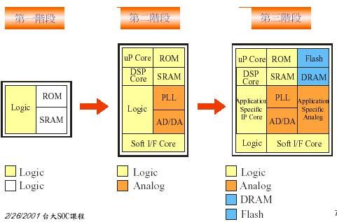
7 SOC pp. 7

8 System-level IC Development pp. 8
9 What s SOC? IP classification Soft IP Firm IP Hard IP IP reusable & benefit Outline SOPC solution on FPGA SOPC design flow pp. 9

10 1. Soft IP: ( Code ) Types of IP 1. Synthesizable HDL description at RTL level 2. Flexible: can be changed to suit an application 3. Technology independent: may be re-synthesized across process 4. Significant IP protection risk pp. 10

11 Types of IP 1. Firm IP: ( synthesizable netlist + structure ) 1. Gate-level netlist optimized structurally and topologically for performance and size 2. Floorplanning or placement without routing pp. 11

12 Types of IP (cont.) 3. Hard IP: ( physical ) 1. Ready for drop in 2. Include layout and timing information 3. Optimized for performance, size, and power 4. IP is easily protected pp. 12
13 Categorizing Reusable Blocks pp. 13

14 Tradeoffs among types of blocks pp. 14
15 What s SOC? IP classification Outline IP reusable & benefit SOPC solution on FPGA SOPC design flow pp. 15

16 Engineering Productivity Gap 1. Engineering productivity has not been keeping up with silicon gate capacity for several years. 2. Companies have been using larger design teams, making engineers work longer hours, etc., but clearly the limit is being reached. pp. 16
17 Why must IP Reuse? pp. 17
18 What s SOC? IP classification IP reusable & benefit Outline SOPC solution on FPGA SOPC design flow pp. 18
19 What is SOPC? Processor Embedded Processor Memory Complete SOPC Solution FPGAHigh- (System-On-a- Programmable- Chip) Logic Performance I/O pp. 19


20 Introduce to SOPC solution Soft embedded processor design & prototyping environment pp. 20

21 Introduce to SOPC solution Hard embedded processor design & prototyping environment pp. 21
22 Excalibur Nios Device Support Performance (MIPS) Future PLD Architectures TM Embedded Core Excalibur MIPS Excalibur ARM Mercury Devices APEX Devices FLEX 10K Devices ACEX Devices 0 pp. 22
23 Flexibility & Scalability Low-Cost High-Performance Embedded Processor Custom DSP Multi-Processor System DSP ESB ESB ESB ESB 75K Gates Available ACEX EP1K K Gates Available ESB ESB ESB ESB ESB ESB ESB ESB APEX EP20K200E 500K Gates Available Excalibur ARM Stripe Excalibur XA10 pp. 23

24 Nios 32-Bit and 16-Bit RISC CPU Peripherals Development Board Development Tools Nios Development Kit pp. 24
25 Nios Embedded Processor Core Configurable Soft Core Processor 32-Bit Pipelined RISC Architecture Large Internal Register File Fully synchronous interface Configurable Data Path 30 to 80 MIPS Performance Dynamic Bus Sizing SRAM FLASH Serial Port Altera PLD PBM CPU Timer UART IRQ Your Design Here 12% of EP20K200E pp. 25
26 What s SOC? IP classification IP reusable & benefit Outline SOPC solution on FPGA SOPC design flow pp. 26
27 Nios System Overview A complete Nios system module contains a Nios embedded processor and its associated system peripherals. The SOPC Builder helps you easily specify options for the Nios system module. Nios system module contains hardware and software sections pp. 27
 Peripheral components Memory Interface RAM, ROM Serial I/O UART PIO(parallel IO)")
28 Nios System Overview(cont.) Peripheral components Memory Interface RAM, ROM Serial I/O UART PIO(parallel IO) Seven Segment LED, LCD User defined Interface Timer pp. 28
29 Nios System Overview(cont.) The SOPC builder let NIOS module easy specified by using wizard Almost constraint can be changed to fit our own design, such as peripheral library. pp. 29
30 Nios System Overview(cont.) Hardware & Software generation Nios system module contains: Hardware : (HDL code) describe the hardware module -download by QuartsII Software : (header file) define c program library to develop your own program -download by NIOS SDK pp. 30
31 Tool Design Flow Configure Processor Peripheral Library Hardware Processor Design Simulation Test Bench Synthesis Place & Route User Design Purchased IP Hardware Configuration File Select Peripherals Generate JTAG Serial Download & Debug Altera PLD Executable Code Software C Header files Custom Library Boot monitor Cygnus/Red Hat GNUPro User Code S/W Libraries RTOS pp. 31
32 Create your design Create project file Create *.BDF file Steps Add SOPC into your design Connect your own block & IO pad to Nios CPU Compile & Pin Assignment Software development Download your design pp. 32

33 Select File => New Project Wizard Create a new project Working Directory Project name Top-level design name Create a new project in the path C:\AVLSI\<your id>\lab2 Click finish pp. 33

34 Create a new schematic Create a *.bdf file, for placing SOPC system, include NIOS CPU & other block Block design file pp. 34
35 Steps Create your design Add SOPC into your design Create CPU Add peripherals Generate hardware & software design Connect your own block & IO pad to Nios CPU Compile & Pin Assignment Software development Download your design pp. 35

36 Create NIOS32 CPU Select symbol from tool menu bar, And click Mega Wizard Plug-In Manager pp. 36

37 Create megafunction SOPC is one block of megafunction Create a new megafunction, to familiar with it s content pp. 37

38 Select Altera SOPC Builder 2.5 and Use SOPC Builder Choose Verilog HDL to perform the soft core CPU pp. 38

39 Double click the component list for adding it into your design Add Components pp. 39
40 Current List of Peripherals UART PIO Timer SPI PWM IDE Keyboard PS2 Mouse VGA Ethernet PCI SRAM SDRAM Flash Compact Flash On-chip RAM On-chip ROM User-Defined pp. 40
41 PIO Peripheral PIO Peripheral 1 to 32-bit Parallel I/O Port Input Only Output Only Bi-directional Port Edge Detection on Inputs Interrupt Generation Mask-able IRQ Source pp. 41
42 User-Defined Interface Interface to Other Peripherals Configures Busses and Timing Adds Port Signals to Design Altera PLD Nios CPU Avalon Bus I/O I/O I/O I/O Nios System Module User I/F External Device pp. 42
43 Addon Component Peripheral components Altera PLD Memory Interface RAM, ROM, flash Serial I/O UART PIO(parallel IO) Seven Segment Nios CPU Avalon Bus I/O I/O I/O I/O LED, LCD User defined Interface Nios System Module User I/F External Device Timer pp. 43

44 The demo board pp. 44

45 Add CPU Choose 32 bit RISC CPU, then click Finish Click finish pp. 45
46 Steps Create your design Add SOPC into your design Create CPU Add peripherals Generate hardware & software design Connect your own block & IO pad to Nios CPU Compile & Pin Assignment Software development Download your design pp. 46


47 Choose On-chip Memory pp. 47

48 GERMS Monitor UART Monitor Program Runs from On-Chip ROM Debugger Runs on Host PC or UNIX Platform Basic Development Facilities: Download Code Burn Flash Examine/Modify Memory Run Programs Debug Monitor pp. 48
49 GERMS G Go E Erase Flash R Relocate M Memory S Motorola S record : Intel Hex record CR show next 64 Bytes of memory Escape Restart GERMS monitor pp. 49


50 Flash memory setting Simulate by Quarts II pp. 50
51 Steps Create your design Add SOPC into your design Create CPU Add peripherals Generate hardware & software design Connect your own block & IO pad to Nios CPU Compile & Pin Assignment Software development Download your design pp. 51

52 SOPC Setup Choose verilog and APEX 20KE in HDL generation pp. 52
 Hardware Design")
53 Generate System Module Software Development Kit (SDK) Hardware Design Synthesis pp. 53
54 What happen after Generate Software nios.h :define the peripheral address :define the memory map Hardware A NIOS CPU module constructed by verilog code pp. 54
 0x00000420) #define na_uart_1_debug_irq 17 #define na_timer_0 ((np_timer *) 0x00000440) #define na_timer_0_irq 18 #define")
55 IO have their addr. Software Generation /* * File: nios.h * * This file is a machine generated address map * for a Nios cpu named cpu. * f:/ /avlsi/r /lab2/nios32.ptf * Generated: :29:11 */ // The Memory Map #define na_uart_1_debug ((np_uart *) 0x ) #define na_uart_1_debug_irq 17 #define na_timer_0 ((np_timer *) 0x ) #define na_timer_0_irq 18 #define na_led_pio ((np_pio *) 0x ) #define na_button_pio ((np_pio *) 0x ) #define na_button_pio_irq 19 #define na_ext_ram ((void *) 0x ) #define na_ext_ram_end ((void *) 0x ) #define na_ext_ram_size ((void *) 0x ) #define na_ext_flash ((void *) 0x ) pp. 55

56 Hardware Genereation After generation, a NIOS module appears in Symbol pp. 56
57 Create your design Steps Add SOPC into your design Connect your own block & IO pad to Nios CPU Compile & Pin Assignment Software development Download your design pp. 57

58 Add IO Pad Use add symbol to add IO pad to schematic. pp. 58
59 Create your design Steps Add SOPC into your design Connect your own block & IO pad to Nios CPU Pin Assignment & Compile Download your design pp. 59

60 Assign Pins Compile first Assign the IO pins to the I/O Interface on develop board Compile then pp. 60
61 Create your design Steps Add SOPC into your design Connect your own block & IO pad to Nios CPU Compile & Pin Assignment Software development Download your design pp. 61
62 Software Develop CPU contains hardware part and software part Hardware part was created above Software part is written in c or c++ language, then compiled into assembly code Take an example for writing c++ program to control CPU change light when press switch pp. 62
63 How to write code Define memory map & peripheral addr led button 0: input 1:output 2:bidrection pp. 63
64 How to write code(cont.) Get data Change led light Write data pp. 64
65 Create your design Steps Add SOPC into your design Connect your own block & IO pad to Nios CPU Compile & Pin Assignment Software development Download your design pp. 65
66 Memory Usage *.srec is downloaded into SRAM, can t still exist after reset Flash memory store the data executed automatically when boot 1Mb Flash Factory APEX Image User APEX Image User Software Data Address APEX SRAM 256Kb ROM pp. 66

67 NIOS SDK UNIX like environment Open from Start Menu/program files/altera/excalibur NIOS 2.0/NIOS SDK Shell pp. 67
68 NIOS Command nios-build: Compile, Assemble & Link Transpose c program into <program>.srec nios-run: Download Executable & Run burn flash with <project>.hexout(hardware) or <program>.flash(software) Download *.srec to SRAM srec2flash: Create Flash-bootable Code Convert <program>.srec to <program>.flash pp. 68
69 Nios Routines nios-build hello.c (nb hello.c) Builds program including compile, link and convert to SREC nios-run hello.srec (nr hello.srec) Downloads using com1 and enters terminal mode nr p com2 hello.srec Downloads using com2 nr x hello.srec Downloads without entering terminal mode nr t Enters terminal mode without download (Ctrl + C to exit) pp. 69
70 Download routine nr <project>.hexout -download hardware design nr <program>.srec design -download software pp. 70
71 NIOS Tutorial LAB Have a C code to generate sine wave and display to 7-segment LED. Program should read data from DIP SW as a value of delay loop. ( pi / 10) pp. 71
72 Homework Use Mega Plug-In Manager to generate NIOS with DIP SW and necessary peripheral device. Use Mega Plug-In Manager to generate a 4 by 4 multiplier. Have a verilog code to decode 8 bit binary to 7- segment. Have a C code to read two 4-bit data from DIP SW and send data to 4 by 4 multiplier. The multiplier output should connect to decoder directly to display answer. Use LA to read answer-data to verify, too. pp. 72
Nios Soft Core Embedded Processor
 Nios Soft Core Embedded Processor June 2000, ver. 1 Data Sheet Features... Preliminary Information Part of Altera s Excalibur TM embedded processor solutions, the Nios TM soft core embedded processor is
Building A Custom System-On-A-Chip
 Building A Custom System-On-A-Chip Only a few years ago, we could only dream about building our very own custom microprocessor system on a chip. The manufacturing cost for producing a custom chip is just
Designing Embedded Processors in FPGAs
 Designing Embedded Processors in FPGAs 2002 Agenda Industrial Control Systems Concept Implementation Summary & Conclusions Industrial Control Systems Typically Low Volume Many Variations Required High
System-on Solution from Altera and Xilinx
 System-on on-a-programmable-chip Solution from Altera and Xilinx Xun Yang VLSI CAD Lab, Computer Science Department, UCLA FPGAs with Embedded Microprocessors Combination of embedded processors and programmable
NIOS CPU Based Embedded Computer System on Programmable Chip
 NIOS CPU Based Embedded Computer System on Programmable Chip 1 Lab Objectives EE8205: Embedded Computer Systems NIOS-II SoPC: PART-I This lab has been constructed to introduce the development of dedicated
NIOS CPU Based Embedded Computer System on Programmable Chip
 1 Objectives NIOS CPU Based Embedded Computer System on Programmable Chip EE8205: Embedded Computer Systems This lab has been constructed to introduce the development of dedicated embedded system based
ECE332, Week 2, Lecture 3. September 5, 2007
 ECE332, Week 2, Lecture 3 September 5, 2007 1 Topics Introduction to embedded system Design metrics Definitions of general-purpose, single-purpose, and application-specific processors Introduction to Nios
ECE332, Week 2, Lecture 3
 ECE332, Week 2, Lecture 3 September 5, 2007 1 Topics Introduction to embedded system Design metrics Definitions of general-purpose, single-purpose, and application-specific processors Introduction to Nios
Nios Development Kit, Stratix Edition
 Nios Development Kit, Stratix Edition User Guide 101 Innovation Drive San Jose, CA 95134 (408) 544-7000 http://www.altera.com Document Version: 1.0 Document Date: January 2003 UG-NIOSSTX-1.0 P25-08785-00
DKAN0011A Setting Up a Nios II System with SDRAM on the DE2
 DKAN0011A Setting Up a Nios II System with SDRAM on the DE2 04 November 2009 Introduction This tutorial details how to set up and instantiate a Nios II system on Terasic Technologies, Inc. s DE2 Altera
Excalibur Device Overview
 May 2002, ver. 2.0 Data Sheet Features... Combination of a world-class RISC processor system with industryleading programmable logic on a single device Industry-standard ARM922T 32-bit RISC processor core
Practical Hardware Debugging: Quick Notes On How to Simulate Altera s Nios II Multiprocessor Systems Using Mentor Graphics ModelSim
 Practical Hardware Debugging: Quick Notes On How to Simulate Altera s Nios II Multiprocessor Systems Using Mentor Graphics ModelSim Ray Duran Staff Design Specialist FAE, Altera Corporation 408-544-7937
Estimating Nios Resource Usage & Performance
 Estimating Nios Resource Usage & Performance in Altera Devices September 2001, ver. 1.0 Application Note 178 Introduction The Excalibur Development Kit, featuring the Nios embedded processor, includes
EMBEDDED SOPC DESIGN WITH NIOS II PROCESSOR AND VHDL EXAMPLES
 EMBEDDED SOPC DESIGN WITH NIOS II PROCESSOR AND VHDL EXAMPLES Pong P. Chu Cleveland State University A JOHN WILEY & SONS, INC., PUBLICATION PREFACE An SoC (system on a chip) integrates a processor, memory
Nios Embedded Processor Development Board
 Nios Embedded Processor Development Board July 2003, ver. 2.2 Data Sheet Introduction Development Board Features Functional Overview This data sheet describes the features and functionality of the Nios
Digital Systems Design. System on a Programmable Chip
 Digital Systems Design Introduction to System on a Programmable Chip Dr. D. J. Jackson Lecture 11-1 System on a Programmable Chip Generally involves utilization of a large FPGA Large number of logic elements
Laboratory Exercise 5
 Laboratory Exercise 5 Bus Communication The purpose of this exercise is to learn how to communicate using a bus. In the designs generated by using Altera s SOPC Builder, the Nios II processor connects
Intelop. *As new IP blocks become available, please contact the factory for the latest updated info.
 A FPGA based development platform as part of an EDK is available to target intelop provided IPs or other standard IPs. The platform with Virtex-4 FX12 Evaluation Kit provides a complete hardware environment
Terasic DE0 Field Programmable Gate Array (FPGA) Development Board
 Development Board") Lecture FPGA-01 DE0 FPGA Development Board and Quartus II 9.1 FPGA Design Software Terasic DE0 Field Programmable Gate Array (FPGA) Development Board 1 May 16, 2013 3 Layout and Components of DE0 May 16,
Lecture FPGA-01 DE0 FPGA Development Board and Quartus II 9.1 FPGA Design Software Terasic DE0 Field Programmable Gate Array (FPGA) Development Board 1 May 16, 2013 3 Layout and Components of DE0 May 16,
Converting.srec Files to.flash Files for Nios Embedded Processor Applications
 White Paper Converting.srec Files to.flash Files for Nios Embedded Processor Applications Introduction The Excalibur Development Kit, featuring the Nios embedded processor, includes the software, hardware,
2001 Altera Corporation (1)
") 2001 Altera Corporation (1) SOPC Design Using ARM-Based Excalibur Devices Outline! ARM-based Devices Overview! Embedded Stripe! Excalibur MegaWizard! Verification Tools Bus Functional Model Full Stripe
2001 Altera Corporation (1) SOPC Design Using ARM-Based Excalibur Devices Outline! ARM-based Devices Overview! Embedded Stripe! Excalibur MegaWizard! Verification Tools Bus Functional Model Full Stripe
Lab 2 EECE473 Computer Organization & Architecture University of Maine
 Lab 2: Verilog Programming Instructor: Yifeng Zhu 50 Points Objectives: 1. Quatus II Programming assignment: PIN assignments, LEDs, switches; 2. Download and test the design on Altera DE2 board 3. Create
Florida State University Libraries
 Florida State University Libraries Electronic Theses, Treatises and Dissertations The Graduate School 2004 Design of Custom Instruction Set for FFT Using FPGA-Based ios Processors Divya Lakshmi Sunkara
Designing with Nios II and SOPC Builder
 Designing with Nios II and SOPC Builder Copyright Altera Corporation The Programmable Solutions Company Devices Stratix II Stratix Stratix GX Cyclone II Cyclone MAX II Devices (continued) Mercury Devices
ARM-Based Embedded Processor Device Overview
 ARM-Based Embedded Processor Device Overview February 2001, ver. 1.2 Data Sheet Features... Industry-standard ARM922T 32-bit RISC processor core operating at up to 200 MHz, equivalent to 210 Dhrystone
)8-,768'HY.LW 2YHUYLHZ. )XMLWVX0LNURHOHNWURQLN*PE+ Am Siebenstein Dreieich-Buchschlag, Germany
8-,768'HY.LW 2YHUYLHZ. )XMLWVX0LNURHOHNWURQLN*PE+ Am Siebenstein Dreieich-Buchschlag, Germany") )8-,768'HY.LW 2YHUYLHZ )XMLWVX0LNURHOHNWURQLN*PE+ Am Siebenstein 6-10 63303 Dreieich-Buchschlag, Germany Revision: V1.0 Date: 05.08.1999 Introduction to FUJITSU Development Kit for 16LX CPU family DevKit16
)8-,768'HY.LW 2YHUYLHZ )XMLWVX0LNURHOHNWURQLN*PE+ Am Siebenstein 6-10 63303 Dreieich-Buchschlag, Germany Revision: V1.0 Date: 05.08.1999 Introduction to FUJITSU Development Kit for 16LX CPU family DevKit16
Introduction to the Altera SOPC Builder Using Verilog Designs. 1 Introduction
 Introduction to the Altera SOPC Builder Using Verilog Designs 1 Introduction This tutorial presents an introduction to Altera s SOPC Builder software, which is used to implement a system that uses the
Introduction to the Altera SOPC Builder Using Verilog Design
 Introduction to the Altera SOPC Builder Using Verilog Design This tutorial presents an introduction to Altera s SOPC Builder software, which is used to implement a system that uses the Nios II processor
Design of Embedded Hardware and Firmware
 Design of Embedded Hardware and Firmware Introduction on "System On Programmable Chip" NIOS II Avalon Bus - DMA Andres Upegui Laboratoire de Systèmes Numériques hepia/hes-so Geneva, Switzerland Embedded
Designing with ALTERA SoC Hardware
 Designing with ALTERA SoC Hardware Course Description This course provides all theoretical and practical know-how to design ALTERA SoC devices under Quartus II software. The course combines 60% theory
New System Solutions for Laser Printer Applications by Oreste Emanuele Zagano STMicroelectronics
 New System Solutions for Laser Printer Applications by Oreste Emanuele Zagano STMicroelectronics Introduction Recently, the laser printer market has started to move away from custom OEM-designed 1 formatter
Non-Volatile Configuration Scheme for the Stratix II EP2S60 DSP Development Board
 Non-Volatile Configuration Scheme for the Stratix II EP2S60 DSP Development Board Qian Liu and S.W. Ellingson October 21, 2008 The Stratix II DSP development board (DSP board) has provided a non-volatile
ECE 111 ECE 111. Advanced Digital Design. Advanced Digital Design Winter, Sujit Dey. Sujit Dey. ECE Department UC San Diego
 Advanced Digital Winter, 2009 ECE Department UC San Diego dey@ece.ucsd.edu http://esdat.ucsd.edu Winter 2009 Advanced Digital Objective: of a hardware-software embedded system using advanced design methodologies
3-D Accelerator on Chip
 3-D Accelerator on Chip Third Prize 3-D Accelerator on Chip Institution: Participants: Instructor: Donga & Pusan University Young-Hee Won, Jin-Sung Park, Woo-Sung Moon Sam-Hak Jin Design Introduction Recently,
The SOCks Design Platform. Johannes Grad
 The SOCks Design Platform Johannes Grad System-on-Chip (SoC) Design Combines all elements of a computer onto a single chip Microprocessor Memory Address- and Databus Periphery Application specific logic
SOPC LAB1. I. Introduction. II. Lab contents. 4-bit count up counter. Advanced VLSI Due Wednesday, 01/08/2003
 SOPC LAB1 I. Introduction The purpose of this lab is to familiarize you with all the items in the kit. This tutorial tells you how to develop FPGA system in Quartus II. You are ready to begin using the
University of Massachusetts Amherst Computer Systems Lab 1 (ECE 354) LAB 1 Reference Manual
 LAB 1 Reference Manual") University of Massachusetts Amherst Computer Systems Lab 1 (ECE 354) LAB 1 Reference Manual Lab 1: Using NIOS II processor for code execution on FPGA Objectives: 1. Understand the typical design flow in
University of Massachusetts Amherst Computer Systems Lab 1 (ECE 354) LAB 1 Reference Manual Lab 1: Using NIOS II processor for code execution on FPGA Objectives: 1. Understand the typical design flow in
The industrial technology is rapidly moving towards ARM based solutions. Keeping this in mind, we are providing a Embedded ARM Training Suite.
 EMBEDDED ARM TRAINING SUITE ARM SUITE INCLUDES ARM 7 TRAINER KIT COMPILER AND DEBUGGER THROUGH JTAG INTERFACE PROJECT DEVELOPMENT SOLUTION FOR ARM 7 e-linux LAB FOR ARM 9 TRAINING PROGRAM INTRODUCTION
NIOS CPU Based Embedded Computer System on Programmable Chip
 NIOS CPU Based Embedded Computer System on Programmable Chip EE8205: Embedded Computer Systems NIOS-II SoPC: PART-II 1 Introduction This lab has been constructed to introduce the development of dedicated
9. Building Memory Subsystems Using SOPC Builder
 9. Building Memory Subsystems Using SOPC Builder QII54006-6.0.0 Introduction Most systems generated with SOPC Builder require memory. For example, embedded processor systems require memory for software
University of Massachusetts Amherst Computer Systems Lab 2 (ECE 354) Spring Lab 1: Using Nios 2 processor for code execution on FPGA
 Spring Lab 1: Using Nios 2 processor for code execution on FPGA") University of Massachusetts Amherst Computer Systems Lab 2 (ECE 354) Spring 2007 Lab 1: Using Nios 2 processor for code execution on FPGA Objectives: After the completion of this lab: 1. You will understand
University of Massachusetts Amherst Computer Systems Lab 2 (ECE 354) Spring 2007 Lab 1: Using Nios 2 processor for code execution on FPGA Objectives: After the completion of this lab: 1. You will understand
Jin-Fu Li. Department of Electrical Engineering. Jhongli, Taiwan
 Chapter 9 Basics of SOC Testing Jin-Fu Li Advanced Reliable Systems (ARES) Lab Department of Electrical Engineering National Central University Jhongli, Taiwan Outline Introduction SOC Test Challenge SOC
PREFACE. Changes to the SOPC Edition
 PREFACE Changes to the SOPC Edition Rapid Prototyping of Digital Systems provides an exciting and challenging laboratory component for undergraduate digital logic and computer design courses using FPGAs
DQ8051. Revolutionary Quad-Pipelined Ultra High performance 8051 Microcontroller Core
 DQ8051 Revolutionary Quad-Pipelined Ultra High performance 8051 Microcontroller Core COMPANY OVERVIEW Digital Core Design is a leading IP Core provider and a System-on-Chip design house. The company was
Celeron EPIC Computer with GUI and Dual Ethernet SBC4685
 Celeron EPIC Computer with GUI and Dual SBC4685 Features Ready to run Celeron/Pentium III computer Color flat-panel support Four serial ports CAN Bus interface PC/104 & PC/104-Plus expansion The SBC4685
Embedded Systems. "System On Programmable Chip" NIOS II Avalon Bus. René Beuchat. Laboratoire d'architecture des Processeurs.
 Embedded Systems "System On Programmable Chip" NIOS II Avalon Bus René Beuchat Laboratoire d'architecture des Processeurs rene.beuchat@epfl.ch 3 Embedded system on Altera FPGA Goal : To understand the
Park Sung Chul. AE MentorGraphics Korea
 PGA Design rom Concept to Silicon Park Sung Chul AE MentorGraphics Korea The Challenge of Complex Chip Design ASIC Complex Chip Design ASIC or FPGA? N FPGA Design FPGA Embedded Core? Y FPSoC Design Considerations
SoC Design Lecture 9: Platform Based Design. Shaahin Hessabi Department of Computer Engineering
 SoC Design Lecture 9: Platform Based Design Shaahin Hessabi Department of Computer Engineering Design Methodologies TDD: Timing-Driven Design BBD: Block-Based B Design PBD: Platform-Based Design 2 Timing-Driven
HyperBus Memory Controller (HBMC) Tutorial
 Tutorial") Synaptic Labs' HyperBus Memory Controller (HBMC) Tutorial T001A: A Qsys based Nios II Reference design with a simple self test of the HyperFlash and HyperRAM device using S/Labs' HBMC IP This tutorial
Synaptic Labs' HyperBus Memory Controller (HBMC) Tutorial T001A: A Qsys based Nios II Reference design with a simple self test of the HyperFlash and HyperRAM device using S/Labs' HBMC IP This tutorial
ESE Back End 2.0. D. Gajski, S. Abdi. (with contributions from H. Cho, D. Shin, A. Gerstlauer)
") ESE Back End 2.0 D. Gajski, S. Abdi (with contributions from H. Cho, D. Shin, A. Gerstlauer) Center for Embedded Computer Systems University of California, Irvine http://www.cecs.uci.edu 1 Technology advantages
ESE Back End 2.0 D. Gajski, S. Abdi (with contributions from H. Cho, D. Shin, A. Gerstlauer) Center for Embedded Computer Systems University of California, Irvine http://www.cecs.uci.edu 1 Technology advantages
IP CORE Design 矽智產設計. C. W. Jen 任建葳.
 IP CORE Design 矽智產設計 C. W. Jen 任建葳 cwjen@twins.ee.nctu.edu.tw Course Contents Introduction to SoC and IP ARM processor core and instruction sets VCI interface, on-chip bus, and platform-based design IP
Digital Integrated Circuits
 Digital Integrated Circuits Lecture 9 Jaeyong Chung Robust Systems Laboratory Incheon National University DIGITAL DESIGN FLOW Chung EPC6055 2 FPGA vs. ASIC FPGA (A programmable Logic Device) Faster time-to-market
V8-uRISC 8-bit RISC Microprocessor AllianceCORE Facts Core Specifics VAutomation, Inc. Supported Devices/Resources Remaining I/O CLBs
 V8-uRISC 8-bit RISC Microprocessor February 8, 1998 Product Specification VAutomation, Inc. 20 Trafalgar Square Nashua, NH 03063 Phone: +1 603-882-2282 Fax: +1 603-882-1587 E-mail: sales@vautomation.com
esi-risc Development Suite Getting Started Guide
 1 Contents 1 Contents 2 2 Overview 3 3 Starting the Integrated Development Environment 4 4 Hello World Tutorial 5 5 Next Steps 8 6 Support 10 Version 2.5 2 of 10 2011 EnSilica Ltd, All Rights Reserved
ARM Processors for Embedded Applications
 ARM Processors for Embedded Applications Roadmap for ARM Processors ARM Architecture Basics ARM Families AMBA Architecture 1 Current ARM Core Families ARM7: Hard cores and Soft cores Cache with MPU or
FPGA for Software Engineers
 FPGA for Software Engineers Course Description This course closes the gap between hardware and software engineers by providing the software engineer all the necessary FPGA concepts and terms. The course
Introduction to Embedded System Design using Zynq
 Introduction to Embedded System Design using Zynq Zynq Vivado 2015.2 Version This material exempt per Department of Commerce license exception TSU Objectives After completing this module, you will be able
AMBA PCI Bridge Quick Start
 AMBA PCI Bridge Quick Start v 2.0 02 Sep 2002 PLDApplications, 1996 2002 Quick Start PLDApplications Europarc Pichaury A2 1330, rue Guillibert 13856 Aix en Provence CEDEX 3 France Web: Email: USA : Intl
Simple Excalibur System
 Excalibur Solutions Simple Excalibur System August 2002, ver. 1.0 Application Note 242 Introduction This application note describes a simple Excalibur system design that consists of software running on
Laboratory Exercise 3 Comparative Analysis of Hardware and Emulation Forms of Signed 32-Bit Multiplication
 Laboratory Exercise 3 Comparative Analysis of Hardware and Emulation Forms of Signed 32-Bit Multiplication Introduction All processors offer some form of instructions to add, subtract, and manipulate data.
Graduate Institute of Electronics Engineering, NTU. ASIC Logic. Speaker: Lung-Hao Chang 張龍豪 Advisor: Prof. Andy Wu 吳安宇教授.
 ASIC Logic Speaker: Lung-Hao Chang 張龍豪 Advisor: Prof. Andy Wu 吳安宇教授 May 21, 2003 PP. 2 Prototyping Goal of This Lab Familiarize with ARM Logic Module (LM) Know how to program LM PP. 3 Introduction ARM
ASIC Logic. Speaker: Juin-Nan Liu. Adopted from National Chiao-Tung University IP Core Design
 ASIC Logic Speaker: Juin-Nan Liu Adopted from National Chiao-Tung University IP Core Design Goal of This Lab Prototyping Familiarize with ARM Logic Module (LM) Know how to program LM Outline Introduction
Copyright 2014 Xilinx
 IP Integrator and Embedded System Design Flow Zynq Vivado 2014.2 Version This material exempt per Department of Commerce license exception TSU Objectives After completing this module, you will be able
System Development Tools for Excalibur Devices
 System Development Tools or Excalibur Devices January 2003, ver. 1.0 Application Note 299 Introduction The Excalibur embedded processor devices achieve a new level o system integration rom the inclusion
Designing with Nios II Processor for Hardware Engineers
 Designing with Nios II Processor for Hardware Engineers Course Description This course provides all theoretical and practical know-how to design ALTERA SoC FPGAs based on the Nios II soft processor under
CPE 200L LABORATORY 4: INTRODUCTION TO DE2 BOARD UNIVERSITY OF NEVADA, LAS VEGAS GOALS: BACKGROUND:
 CPE 200L LABORATORY 4: INTRODUCTION TO DE2 BOARD DEPARTMENT OF ELECTRICAL AND COMPUTER ENGINEERING UNIVERSITY OF NEVADA, LAS VEGAS GOALS: Getting familiar with DE2 board installation, properties, usage.
ECE-6170 Embedded Systems Laboratory Exercise 3
 ECE-6170 Embedded Systems Laboratory Exercise 3 The purpose of this exercise is to learn how to connect simple input and output devices to an FPGA chip and use the Nios II processor to interface with parallel
acret Ameya Centre for Robotics & Embedded Technology Syllabus for Diploma in Embedded Systems (Total Eight Modules-4 Months -320 Hrs.
 acret Ameya Centre for Robotics & Embedded Technology Syllabus for Diploma in Embedded Systems (Total Eight Modules-4 Months -320 Hrs.) Module 0 Introduction Introduction to Embedded Systems, Real Time
QUARTUS II Altera Corporation
 QUARTUS II Quartus II Design Flow Design Entry Timing Constraints Synthesis Placement and Routing Timing, Area, Power Optimization Timing and Power Analyzer Optimized Design 2 Can I still use a Processor?
Introduction to VHDL Design on Quartus II and DE2 Board
 ECP3116 Digital Computer Design Lab Experiment Duration: 3 hours Introduction to VHDL Design on Quartus II and DE2 Board Objective To learn how to create projects using Quartus II, design circuits and
HyperBus Memory Controller (HBMC) Tutorial
 Tutorial") Synaptic Labs' HyperBus Memory Controller (HBMC) Tutorial T005B: A Qsys based Nios II Reference design with a simple application running from HyperFlash and HyperRAM device using S/Labs' HBMC IP. The HyperRAM
Synaptic Labs' HyperBus Memory Controller (HBMC) Tutorial T005B: A Qsys based Nios II Reference design with a simple application running from HyperFlash and HyperRAM device using S/Labs' HBMC IP. The HyperRAM
Programming in the MAXQ environment
 AVAILABLE The in-circuit debugging and program-loading features of the MAXQ2000 microcontroller combine with IAR s Embedded Workbench development environment to provide C or assembly-level application
Introducing the Spartan-6 & Virtex-6 FPGA Embedded Kits
 Introducing the Spartan-6 & Virtex-6 FPGA Embedded Kits Overview ß Embedded Design Challenges ß Xilinx Embedded Platforms for Embedded Processing ß Introducing Spartan-6 and Virtex-6 FPGA Embedded Kits
386EX PC/104 Computer with CompactFlash and PCMCIA SBC1390
 386EX PC/104 Computer with CompactFlash and PCMCIA SBC1390 Features Small, low cost, ready to run 386EX, 25 or 33MHz Up to 32MB DRAM CompactFlash connector Optional PC Card interface for Wi-Fi, modem,
DE2 Board & Quartus II Software
 January 23, 2015 Contact and Office Hours Teaching Assistant (TA) Sergio Contreras Office Office Hours Email SEB 3259 Tuesday & Thursday 12:30-2:00 PM Wednesday 1:30-3:30 PM contre47@nevada.unlv.edu Syllabus
Melon S3 FPGA Development Board Product Datasheet
 Melon S3 FPGA Development Board Product Datasheet The Melon S3 FPGA is open-source, expandable development board perfect for the learning digital circuit design and prototyping of your unique ideas. You
Project design tutorial (I)
") Project design tutorial (I) Design or project specifications Divide the project or system into blocks or subsystems (top-down design) (hierarchical design) Analogue subsystem Mixed-signal subsystem Digital
Project design tutorial (I) Design or project specifications Divide the project or system into blocks or subsystems (top-down design) (hierarchical design) Analogue subsystem Mixed-signal subsystem Digital
System-on-a-Programmable-Chip (SOPC) Development Board
 Development Board") System-on-a-Programmable-Chip (SOPC) Development Board Solution Brief 47 March 2000, ver. 1 Target Applications: Embedded microprocessor-based solutions Family: APEX TM 20K Ordering Code: SOPC-BOARD/A4E
System-on-a-Programmable-Chip (SOPC) Development Board Solution Brief 47 March 2000, ver. 1 Target Applications: Embedded microprocessor-based solutions Family: APEX TM 20K Ordering Code: SOPC-BOARD/A4E
Chapter 2 Getting Hands on Altera Quartus II Software
 Chapter 2 Getting Hands on Altera Quartus II Software Contents 2.1 Installation of Software... 20 2.2 Setting Up of License... 21 2.3 Creation of First Embedded System Project... 22 2.4 Project Building
FPGA Development Board Hardware and I/O Features
 CHAPTER 2 FPGA Development Board Hardware and I/O Features Photo: The Altera DE1 board contains a Cyclone II FPGA, external SRAM, SDRAM & Flash memory, and a wide assortment of I/O devices and connectors.
Revolutionary Quad-Pipelined Ultra High Performance 16/32-bit Microcontroller v. 6.05
 DQ80251 Revolutionary Quad-Pipelined Ultra High Performance 16/32-bit Microcontroller v. 6.05 O V E R V I E W DQ80251 is a revolutionary Quad-Pipelined ultrahigh performance, speed optimized soft core,
Full Linux on FPGA. Sven Gregori
 Full Linux on FPGA Sven Gregori Enclustra GmbH FPGA Design Center Founded in 2004 7 engineers Located in the Technopark of Zurich FPGA-Vendor independent Covering all topics
April 2002, Version 1.1. Component. PTF File. Component. Component GUI Wizards. Generation. System PTF file Files and Libraries.
 SOPC Builder April 2002, Version 1.1 Data Sheet Introduction SOPC Builder is a tool for composing bus-based systems out of library components such as CPUs, memory interfaces, and peripherals. SOPC Builder
ALTERA FPGAs Architecture & Design
 ALTERA FPGAs Architecture & Design Course Description This course provides all theoretical and practical know-how to design programmable devices of ALTERA with QUARTUS-II design software. The course combines
Advanced 486/586 PC/104 Embedded PC SBC1491
 Advanced 486/586 PC/104 Embedded PC SBC1491 Features Ready to run 486/586 computer Small PC/104 format DiskOnChip, 64MB RAM On-board accelerated VGA COM1, COM2, KBD, mouse 10BASE-T Ethernet port PC/104
Somes French translations :
 1 RB - EPFL/IC/LAP - A2012 Embedded systems Somes French translations : Systèmes embarqués Systèmes enrobés Systèmes enfouis Embedded systems, definition There is no formal definition of an embedded system,
Advanced Embedded Systems
 Advanced Embedded Systems Practical & Professional Training on Advanced Embedded System Course Objectives : 1. To provide professional and industrial standard training which will help the students to get
9. PIO Core. Core Overview. Functional Description
 9. PIO Core NII51007-9.0.0 Core Overview The parallel input/output (PIO) core with Avalon interface provides a memory-mapped interface between an Avalon Memory-Mapped (Avalon-MM) slave port and general-purpose
Fujitsu System Applications Support. Fujitsu Microelectronics America, Inc. 02/02
 Fujitsu System Applications Support 1 Overview System Applications Support SOC Application Development Lab Multimedia VoIP Wireless Bluetooth Processors, DSP and Peripherals ARM Reference Platform 2 SOC
Diploma in Embedded Systems
 Diploma in Embedded Systems Duration: 5 Months[5 days a week,3 hours a day, Total 300 hours] Module 1: 8051 Microcontroller in Assemble Language Characteristics of Embedded System Overview of 8051 Family
Rapidly Developing Embedded Systems Using Configurable Processors
 Class 413 Rapidly Developing Embedded Systems Using Configurable Processors Steven Knapp (sknapp@triscend.com) (Booth 160) Triscend Corporation www.triscend.com Copyright 1998-99, Triscend Corporation.
TECHNICAL UNIVERSITY OF KOŠICE
 TECHNICAL UNIVERSITY OF KOŠICE Faculty of Electrical Engineering and Informatics Department of Electronics and Multimedia Communications MASTER S THESIS Conception of Connection of Embedded Processor to
FPGA Based Digital Design Using Verilog HDL
 FPGA Based Digital Design Using Course Designed by: IRFAN FAISAL MIR ( Verilog / FPGA Designer ) irfanfaisalmir@yahoo.com * Organized by Electronics Division Integrated Circuits Uses for digital IC technology
CHAPTER 1 Introduction of the tnano Board CHAPTER 2 tnano Board Architecture CHAPTER 3 Using the tnano Board... 8
 CONTENTS CHAPTER 1 Introduction of the tnano Board... 2 1.1 Features...2 1.2 About the KIT...4 1.3 Getting Help...4 CHAPTER 2 tnano Board Architecture... 5 2.1 Layout and Components...5 2.2 Block Diagram
SECURE PARTIAL RECONFIGURATION OF FPGAs. Amir S. Zeineddini Kris Gaj
 SECURE PARTIAL RECONFIGURATION OF FPGAs Amir S. Zeineddini Kris Gaj Outline FPGAs Security Our scheme Implementation approach Experimental results Conclusions FPGAs SECURITY SRAM FPGA Security Designer/Vendor
ERIKA Enterprise Multicore Tutorial. for the Altera Nios II platform
 ERIKA Enterprise Multicore Tutorial for the Altera Nios II platform version: 1.0.1 May 27, 2009 About Evidence S.r.l. Evidence is a spin-off company of the ReTiS Lab of the Scuola Superiore S. Anna, Pisa,
CMPE 415 Programmable Logic Devices Introduction
 Department of Computer Science and Electrical Engineering CMPE 415 Programmable Logic Devices Introduction Prof. Ryan Robucci What are FPGAs? Field programmable Gate Array Typically re programmable as
HARDWARE SECURITY. EEC 492/592, CIS 493 Hands-on Experience on Computer System Security Chan Yu Cleveland State University
 HARDWARE SECURITY EEC 492/592, CIS 493 Hands-on Experience on Computer System Security Chan Yu Cleveland State University CONTENTS Overview of Hardware security Basics FPGA (Field Programmable Gate Array)
HyperBus Memory Controller (HBMC) Tutorial
 Tutorial") Synaptic Labs' HyperBus Memory Controller (HBMC) Tutorial T005C: A Qsys based Nios II Reference design with a simple HyperFlash test device using S/Labs' HBMC IP and S/Labs' Memory Region Mapper IP This
Synaptic Labs' HyperBus Memory Controller (HBMC) Tutorial T005C: A Qsys based Nios II Reference design with a simple HyperFlash test device using S/Labs' HBMC IP and S/Labs' Memory Region Mapper IP This
Core Peripherals. Speaker: Tzu-Wei Tseng. Adopted from National Chiao-Tung University IP Core Design. SOC Consortium Course Material
 Core Peripherals Speaker: Tzu-Wei Tseng Adopted from National Chiao-Tung University IP Core Design SOC Consortium Course Material Goal of This Lab Familiarize with ARM Hardware Development Environment