Read Disturb Errors in MLC NAND Flash Memory: Characterization, Mitigation, and Recovery
|
|
|
- Sheila Rice
- 6 years ago
- Views:
Transcription


1 Read Disturb Errors in MLC NAND Flash Memory: Characterization, Mitigation, and Recovery Yu Cai, Yixin Luo, Saugata Ghose, Erich F. Haratsch*, Ken Mai, Onur Mutlu Carnegie Mellon University, *Seagate Technology
2 Executive Summary Read disturb errors limit flash memory lifetime today Apply a high pass-through voltage (V pass )to multiple pages on a read We characterize read disturb on real NAND flash chips Slightly lowering V pass greatly reduces read disturb errors Some flash cells are more prone to read disturb Technique 1: Mitigate read disturb errors online V pass Tuning dynamically finds and applies a lowered V pass Flash memory lifetime improves by 21% Technique 2: Recover after failure to prevent data loss Read Disturb Oriented Error Recovery (RDR) selectively corrects cells more susceptible to read disturb errors Reduces raw bit error rate (RBER) by up to 36% 2
3 Outline Background (Problem and Goal) Key Experimental Observations Mitigation: V pass Tuning Recovery: Read Disturb Oriented Error Recovery Conclusion 3
4 Outline Background (Problem and Goal) Key Experimental Observations Mitigation: V pass Tuning Recovery: Read Disturb Oriented Error Recovery Conclusion 4

5 NAND Flash Memory Background Page 0 Page 1 Page 2 Read Pass Pass Page 256 Page 257 Page 258 Flash Memory Page M Page M+1 Page M+2 Block 0 Block 1 Block N Page 255 Pass Page 511 Page M+255 Flash Controller 5
6 Column Flash Cell Array Block X Row Page Y Sense Amplifiers Sense Amplifiers 6
7 Flash Cell Floating Gate Drain Gate V th = 2.5 V Source Floating Gate Transistor (Flash Cell) 7
8 Flash Read V read = 2.5 V V th = V read = 2.5 V V th = 2 V 3V Gate 1 0 8
9 Flash Pass-Through V pass = 5 V V th = 2 V Gate V pass = 5 V V th = 3V 1 1 9
10 Read from Flash Cell Array V pass = 5.0 V Pass (5V) 3.0V 3.8V 3.9V 4.8V Page 1 V read = 2.5 V Read (2.5V) 3.5V 2.9V 2.4V 2.1V Page 2 V pass = 5.0 V Pass (5V) 2.2V 4.3V 4.6V 1.8V Page 3 V pass = 5.0 V Pass (5V) 3.5V 2.3V 1.9V 4.3V Page 4 Correct values for page 2: 10
11 Read Disturb Problem: Weak Programming Effect Pass (5V) 3.0V 3.8V 3.9V 4.8V Page 1 Pass (5V) 3.5V 2.9V 2.4V 2.1V Page 2 Read (2.5V) 2.2V 4.3V 4.6V 1.8V Page 3 Pass (5V) 3.5V 2.3V 1.9V 4.3V Page 4 Repeatedly read page 3 (or any page other than page 2) 11
12 Read Disturb Problem: Weak Programming Effect V pass = 5.0 V 3.0V 3.8V 3.9V 4.8V Page 1 V read = 2.5 V 3.5V 2.9V 2.4V 2.6V 2.1V Page 2 V pass = 5.0 V 2.2V 4.3V 4.6V 1.8V Page 3 V pass = 5.0 V 3.5V 2.3V 1.9V 4.3V Page 4 Incorrect values from page 2: High pass-through voltage induces weak-programming effect 12
13 Read disturb errors: Reading from one page can alter the values stored in other unread pages Goal: Mitigate and Recover Read Disturb Errors 13
14 Outline Background (Problem and Goal) Key Experimental Observations Mitigation: V pass Tuning Recovery: Read Disturb Oriented Error Recovery Conclusion 14
![Methodology FPGA-based flash memory testing platform [Cai+, FCCM 11] Real 20- to](/docs-images/79/79668336/images/15-0.jpg "24-nm MLC NAND flash chips 0 to 1M read disturbs 0 to 15K Program/Erase Cycles")
15 Methodology FPGA-based flash memory testing platform [Cai+, FCCM 11] Real 20- to 24-nm MLC NAND flash chips 0 to 1M read disturbs 0 to 15K Program/Erase Cycles (PEC) 15
16 PDF Read Disturb Effect on V th Distribution (No Read Disturbs) 0.25M Read Disturbs 0.5M Read Disturbs 1M Read Disturbs ER state P1 state V th gradually increases with read disturb counts P2 state P3 state Normalized Threshold Voltage 16
17 Other Experimental Observations Lower threshold voltage states are affected more by read disturb Wear-out increases read disturb effect 17

18 Normalized Tolerable Read Disturb Count Key Observation 1: Slightly lowering V pass greatly reduces read disturb errors Reducing The Pass-Through Voltage % 1% 2% 3% 4% 5% 6% Percentage of Vpass Reduction 18
19 Outline Background (Problem and Goal) Key Experimental Observations Mitigation: V pass Tuning Recovery: Read Disturb Oriented Error Recovery Conclusion 19
20 Read Disturb Mitigation: V pass Tuning Key Idea: Dynamically find and apply a lowered V pass Trade-off for lowering V pass +Allows more read disturbs Induces more read errors 20
21 Read Errors Induced by V pass Reduction Reducing V pass to 4.9V V pass = 4.9 V 3.0V 3.8V 3.9V 4.8V Page 1 V read = 2.5 V 3.5V 2.9V 2.4V 2.1V Page 2 V pass = 4.9 V 2.2V 4.3V 4.6V 1.8V Page 3 V pass = 4.9 V 3.5V 2.3V 1.9V 4.3V Page
22 Read Errors Induced by V pass Reduction Reducing V pass to 4.7V V pass = 4.7 V 3.0V 3.8V 3.9V 4.8V Page 1 V read = 2.5 V 3.5V 2.9V 2.4V 2.1V Page 2 V pass = 4.7 V 2.2V 4.3V 4.6V 1.8V Page 3 V pass = 4.7 V 3.5V 2.3V 1.9V 4.3V Page 4 Incorrect values from page 2:

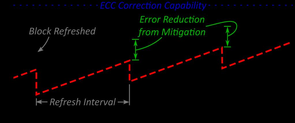
23 RBER Utilizing the Unused ECC Capability ECC Correction Capability Unused ECC capability N-day Retention 1. Huge unused ECC correction capability can be used to tolerate read errors 2. Unused ECC capability decreases over time Dynamically adjust V pass so that read errors fully utilize the unused ECC capability 23
24 V pass Reduction Trade-Off Summary Conservatively set V pass to a high voltage Accumulates more read disturb errors at the end of each refresh interval +No read errors Dynamically adjust V pass to unused ECC capability + Minimize read disturb errors ocontrol read errors to be tolerable by ECC oif read errors exceed ECC capability, read again with a higher V pass to correct read errors 24
25 V pass Tuning Steps Perform once for each block every day: 1. Estimate unused ECC capability 2. Aggressively reduce V pass until read errors exceeds ECC capability 3. Gradually increase V pass until read error just becomes less than ECC capability 25
26 Evaluation of V pass Tuning 19 real workload I/O traces Assume 7-day refresh period Similar methodology as before to determine acceptable V pass reduction Overhead for a 512 GB flash drive: 128 KB storage overhead for per-block V pass setting and worst-case page sec/day average V pass Tuning overhead 26
27 homes web-vm mail mds rsrch prn web stg ts proj src wdev usr postmark hm cello99 websearch financial prxy P/E Cycle Lifetime V pass Tuning Lifetime Improvements Baseline VVpass Tuning Average lifetime improvement: 21.0% 27
28 Outline Background (Problem and Goal) Key Experimental Observations Mitigation: V pass Tuning Recovery: Read Disturb Oriented Error Recovery Conclusion 28
29 Read Disturb Resistance DF Disturb-Resistant R N read disturbs Disturb-Prone P N read disturbs Normalized V th 29
30 DF Observation 2: Some Flash Cells Are More Prone to Read Disturb After 250K read disturb: Disturb-prone cells have higher threshold voltages ER P1 Disturb-resistant cells have lower threshold voltages R P R Disturb-prone ER state P R P R Disturb-resistant P1 state P Normalized V th 30
31 Read Disturb Oriented Error Recovery (RDR) Triggered by an uncorrectable flash error Back up all valid data in the faulty block Disturb the faulty page 100K times (more) Compare V th s before and after read disturb Select cells susceptible to flash errors (V ref σ<v th <V ref σ) Predict among these susceptible cells Cells with more V th shifts are disturb-prone Higher V th state Cells with less V th shifts are disturb-resistant Lower V th state 31
32 RBER RDR Evaluation No Recovery RDR 0 0.2M 0.4M 0.6M 0.8M 1M Read Disturb Count Reduce total error counts up to 1M read disturbs ECC can be used to correct the remaining errors 32
33 Outline Background (Problem and Goal) Key Experimental Observations Mitigation: V pass Tuning Recovery: Read Disturb Oriented Error Recovery Conclusion 33
34 Executive Summary Read disturb errors limit flash memory lifetime today Apply a high pass-through voltage (V pass )to multiple pages on a read We characterize read disturb on real NAND flash chips Slightly lowering V pass greatly reduces read disturb errors Some flash cells are more prone to read disturb Technique 1: Mitigate read disturb errors online V pass Tuning dynamically finds and applies a lowered V pass Flash memory lifetime improves by 21% Technique 2: Recover after failure to prevent data loss Read Disturb Oriented Error Recovery (RDR) selectively corrects cells more susceptible to read disturb errors Reduces raw bit error rate (RBER) by up to 36% 34
35 Read Disturb Errors in MLC NAND Flash Memory: Characterization, Mitigation, and Recovery Yu Cai, Yixin Luo, Saugata Ghose, Erich F. Haratsch*, Ken Mai, Onur Mutlu Carnegie Mellon University, *Seagate Technology
36 Raw Bit Error Rate (RBER) Slower Faster Read Disturb Induced RBER Increases Faster with Higher PEC K 40K 60K 80K 100K Read Disturb Count PEC Slope 15K K K K K K K
37 Norm. Vth Mean Norm. Vth Standard Deviation Threshold Voltage Increases with Read Disturb Count Read Disturb Count (Millions) Read Disturb Count (Millions) Showing results for P1 8K PEC, other states have similar trends 37
38 Norm. Vth Mean Norm. Vth Mean Lower Voltage States Are More Prone to Read Disturb ER State Read Disturb Count (Millions) P1 State Read Disturb Count (Millions) 38

39 RBER Reducing V pass Increases Tolerable Read Disturb % 99% 98% Count 97% 100% V pass 99% V pass 98% V pass 97% V pass 96% V pass 95% V pass 94% V pass Read Disturb Count 96% 95% 94% Pct. V pass Value 100% 99% 98% 97% 96% 95% 94% Rd. Disturb. Cnt. 1x 1.7x 6.8x 22x 100x 470x 1300x 39
40 Pass-Through Voltage Reduction Induced Read Error Addl. RBER Due to Reduced V pass day 1-day 2-day 6-day 9-day 17-day 21-day Relaxed V pass 40
41 Read Errors Induced by V pass Reduction Will generate a read error only if: Max(V th ) > V pass Correct read value is 1 These errors do not affect lifetime can usually be tolerated by the unused ECC capability These errors are temporary can be corrected (if necessary) by reading with the default V pass 41

42 Illustration of V pass Tuning Results 42


43 Some Flash Cells Are More Prone to Read Disturb Predict to be P1 state - Area I is correct - Area II is 50/50 Predict to be ER state - Area III is correct - Area IV is 50/50 Showing V th with 8K PEC from 250K to 350K read disturbs 43
Vulnerabilities in MLC NAND Flash Memory Programming: Experimental Analysis, Exploits, and Mitigation Techniques
 Vulnerabilities in MLC NAND Flash Memory Programming: Experimental Analysis, Exploits, and Mitigation Techniques Yu Cai, Saugata Ghose, Yixin Luo, Ken Mai, Onur Mutlu, Erich F. Haratsch February 6, 2017
Data Retention in MLC NAND Flash Memory: Characterization, Optimization, and Recovery
 Data Retention in MLC NAND Flash Memory: Characterization, Optimization, and Recovery Yu Cai, Yixin Luo, Erich F. Haratsch*, Ken Mai, Onur Mutlu Carnegie Mellon University, *LSI Corporation 1 Many use
Read Disturb Errors in MLC NAND Flash Memory: Characterization, Mitigation, and Recovery
 Carnegie Mellon University Research Showcase @ CMU Department of Electrical and Computer Engineering Carnegie Institute of Technology 6-2015 Read Disturb Errors in MLC NAND Flash Memory: Characterization,
Improving the Reliability of Chip-Off Forensic Analysis of NAND Flash Memory Devices. Aya Fukami, Saugata Ghose, Yixin Luo, Yu Cai, Onur Mutlu
 Improving the Reliability of Chip-Off Forensic Analysis of NAND Flash Memory Devices Aya Fukami, Saugata Ghose, Yixin Luo, Yu Cai, Onur Mutlu 1 Example Target Devices for Chip-Off Analysis Fire damaged
Increasing NAND Flash Endurance Using Refresh Techniques
 Increasing NAND Flash Endurance Using Refresh Techniques Yu Cai 1, Gulay Yalcin 2, Onur Mutlu 1, Erich F. Haratsch 3, Adrian Cristal 2, Osman S. Unsal 2 and Ken Mai 1 DSSC, Carnegie Mellon University 1
HeatWatch Yixin Luo Saugata Ghose Yu Cai Erich F. Haratsch Onur Mutlu
 HeatWatch Improving 3D NAND Flash Memory Device Reliability by Exploiting Self-Recovery and Temperature Awareness Yixin Luo Saugata Ghose Yu Cai Erich F. Haratsch Onur Mutlu Storage Technology Drivers
Improving 3D NAND Flash Memory Lifetime by Tolerating Early Retention Loss and Process Variation
 Improving 3D NAND Flash Memory Lifetime by Tolerating Early Retention Loss and Process Variation YIXIN LUO, Carnegie Mellon University SAUGATA GHOSE, Carnegie Mellon University YU CAI, SK Hynix, Inc. ERICH
arxiv: v1 [cs.ar] 8 May 2018
![arxiv: v1 [cs.ar] 8 May 2018](/thumbs/84/90636678.jpg "arxiv: v1 [cs.ar] 8 May 2018") Read Disturb Errors in MLC NAND Flash Memory Yu Cai 1 Yixin Luo 1 Saugata Ghose 1 Erich F. Haratsch 2 Ken Mai 1 Onur Mutlu 3,1 1 Carnegie Mellon University 2 Seagate Technology 3 ETH Zürich arxiv:185.3283v1
Read Disturb Errors in MLC NAND Flash Memory Yu Cai 1 Yixin Luo 1 Saugata Ghose 1 Erich F. Haratsch 2 Ken Mai 1 Onur Mutlu 3,1 1 Carnegie Mellon University 2 Seagate Technology 3 ETH Zürich arxiv:185.3283v1
HeatWatch: Improving 3D NAND Flash Memory Device Reliability by Exploiting Self-Recovery and Temperature Awareness
 HeatWatch: Improving 3D NAND Flash Memory Device Reliability by Exploiting Self-Recovery and Temperature Awareness Yixin Luo Saugata Ghose Yu Cai Erich F. Haratsch Onur Mutlu Carnegie Mellon University
Data Retention in MLC NAND Flash Memory: Characterization, Optimization, and Recovery
 Carnegie Mellon University Research Showcase @ CMU Department of Electrical and Computer Engineering Carnegie Institute of Technology 2-2015 Data Retention in MLC NAND Flash Memory: Characterization, Optimization,
Enabling Accurate and Practical Online Flash Channel Modeling for Modern MLC NAND Flash Memory
 1 Enabling Accurate and Practical Online Flash Channel Modeling for Modern MLC NAND Flash Memory Yixin Luo, Saugata Ghose, Yu Cai, Erich F Haratsch, Onur Mutlu Abstract NAND flash memory is a widely-used
Error Analysis and Management for MLC NAND Flash Memory
 Error Analysis and Management for MLC NAND Flash Memory Onur Mutlu onur@cmu.edu (joint work with Yu Cai, Gulay Yalcin, Eric Haratsch, Ken Mai, Adrian Cristal, Osman Unsal) August 7, 2014 Flash Memory Summit
Reducing MLC Flash Memory Retention Errors through Programming Initial Step Only
 Reducing MLC Flash Memory Retention Errors through Programming Initial Step Only Wei Wang 1, Tao Xie 2, Antoine Khoueir 3, Youngpil Kim 3 1 Computational Science Research Center, San Diego State University
Amnesic Cache Management for Non-Volatile Memory
 Amnesic Cache Management for Non-Volatile Memory Dongwoo Kang, Seungjae Baek, Jongmoo Choi Dankook University, South Korea {kangdw, baeksj, chiojm}@dankook.ac.kr Donghee Lee University of Seoul, South
DPA: A data pattern aware error prevention technique for NAND flash lifetime extension
 DPA: A data pattern aware error prevention technique for NAND flash lifetime extension *Jie Guo, *Zhijie Chen, **Danghui Wang, ***Zili Shao, *Yiran Chen *University of Pittsburgh **Northwestern Polytechnical
arxiv: v2 [cs.ar] 5 Jan 2018
![arxiv: v2 [cs.ar] 5 Jan 2018](/thumbs/74/69799077.jpg "arxiv: v2 [cs.ar] 5 Jan 2018") 1 Errors in Flash-Memory-Based Solid-State Drives: Analysis, Mitigation, and Recovery YU CAI, SAUGATA GHOSE Carnegie Mellon University arxiv:1711.11427v2 [cs.ar] 5 Jan 2018 ERICH F. HARATSCH Seagate Technology
1 Errors in Flash-Memory-Based Solid-State Drives: Analysis, Mitigation, and Recovery YU CAI, SAUGATA GHOSE Carnegie Mellon University arxiv:1711.11427v2 [cs.ar] 5 Jan 2018 ERICH F. HARATSCH Seagate Technology
Reducing DRAM Latency at Low Cost by Exploiting Heterogeneity. Donghyuk Lee Carnegie Mellon University
 Reducing DRAM Latency at Low Cost by Exploiting Heterogeneity Donghyuk Lee Carnegie Mellon University Problem: High DRAM Latency processor stalls: waiting for data main memory high latency Major bottleneck
Improving LDPC Performance Via Asymmetric Sensing Level Placement on Flash Memory
 Improving LDPC Performance Via Asymmetric Sensing Level Placement on Flash Memory Qiao Li, Liang Shi, Chun Jason Xue Qingfeng Zhuge, and Edwin H.-M. Sha College of Computer Science, Chongqing University
Error Characterization, Mitigation, and Recovery in Flash-Memory-Based Solid-State Drives
 Error Characterization, Mitigation, and Recovery in Flash-Memory-Based Solid-State Drives This paper reviews the most recent advances in solid-state drive (SSD) error characterization, mitigation, and
Design-Induced Latency Variation in Modern DRAM Chips:
 Design-Induced Latency Variation in Modern DRAM Chips: Characterization, Analysis, and Latency Reduction Mechanisms Donghyuk Lee 1,2 Samira Khan 3 Lavanya Subramanian 2 Saugata Ghose 2 Rachata Ausavarungnirun
Understanding Reduced-Voltage Operation in Modern DRAM Devices
 Understanding Reduced-Voltage Operation in Modern DRAM Devices Experimental Characterization, Analysis, and Mechanisms Kevin Chang A. Giray Yaglikci, Saugata Ghose,Aditya Agrawal *, Niladrish Chatterjee
arxiv: v3 [cs.ar] 22 Sep 2017
![arxiv: v3 [cs.ar] 22 Sep 2017](/thumbs/71/65778103.jpg "arxiv: v3 [cs.ar] 22 Sep 2017") Appears in Proceedings of the IEEE, September 2017. Error Characterization, Mitigation, and Recovery in Flash-Memory-Based Solid-State Drives Yu Cai Saugata Ghose Erich F. Haratsch Yixin Luo Onur Mutlu
Appears in Proceedings of the IEEE, September 2017. Error Characterization, Mitigation, and Recovery in Flash-Memory-Based Solid-State Drives Yu Cai Saugata Ghose Erich F. Haratsch Yixin Luo Onur Mutlu
NAND Flash Basics & Error Characteristics
 NAND Flash Basics & Error Characteristics Why Do We Need Smart Controllers? Thomas Parnell, Roman Pletka IBM Research - Zurich Santa Clara, CA 1 Agenda Part I. NAND Flash Basics Device Architecture (2D
Health-Binning Maximizing the Performance and the Endurance of Consumer-Level NAND Flash
 Health-Binning Maximizing the Performance and the Endurance of Consumer-Level NAND Flash Roman Pletka, Saša Tomić IBM Research Zurich Systor 2016, Haifa, Israel June 6, 2016 1 Outline and Motivation Introduction
Self-Adaptive NAND Flash DSP
 Self-Adaptive NAND Flash DSP Wei Xu 2018/8/9 Outline NAND Flash Data Error Recovery Challenges of NAND Flash Data Integrity A Self-Adaptive DSP Technology to Improve NAND Flash Memory Data Integrity 6
arxiv: v1 [cs.ar] 12 Aug 2018
![arxiv: v1 [cs.ar] 12 Aug 2018](/thumbs/93/111052503.jpg "arxiv: v1 [cs.ar] 12 Aug 2018") arxiv:1808.04016v1 [cs.ar] 12 Aug 2018 Architectural Techniques for Improving NAND Flash Memory Reliability Yixin Luo CMU-CS-18-101 August 2018 School of Computer Science Carnegie Mellon University Pittsburgh,
arxiv:1808.04016v1 [cs.ar] 12 Aug 2018 Architectural Techniques for Improving NAND Flash Memory Reliability Yixin Luo CMU-CS-18-101 August 2018 School of Computer Science Carnegie Mellon University Pittsburgh,
ECC Approach for Correcting Errors Not Handled by RAID Recovery
 ECC Approach for Correcting Errors Not Handled by RAID Recovery Jeff Yang Siliconmotion Flash Memory Summit 27 Note: All the material are the concept proof and simulation.s It is not the real Siliconmotion
Controller Concepts for 1y/1z nm and 3D NAND Flash
 Controller Concepts for 1y/1z nm and 3D NAND Flash Erich F. Haratsch Santa Clara, CA 1 NAND Evolution Planar NAND scaling is coming to an end in the sub- 20nm process 15nm and 16nm NAND are the latest
Architectural Techniques for Improving NAND Flash Memory Reliability. Yixin Luo
 Architectural Techniques for Improving NAND Flash Memory Reliability Yixin Luo CMU-CS-18-101 March 2018 School of Computer Science Carnegie Mellon University Pittsburgh, PA 15213 Thesis Committee Onur
NAND Flash Memory. Jinkyu Jeong Computer Systems Laboratory Sungkyunkwan University
 NAND Flash Memory Jinkyu Jeong (Jinkyu@skku.edu) Computer Systems Laboratory Sungkyunkwan University http://csl.skku.edu ICE3028: Embedded Systems Design, Fall 2018, Jinkyu Jeong (jinkyu@skku.edu) Flash
Could We Make SSDs Self-Healing?
 Could We Make SSDs Self-Healing? Tong Zhang Electrical, Computer and Systems Engineering Department Rensselaer Polytechnic Institute Google/Bing: tong rpi Santa Clara, CA 1 Introduction and Motivation
SoftMC A Flexible and Practical Open-Source Infrastructure for Enabling Experimental DRAM Studies
 SoftMC A Flexible and Practical Open-Source Infrastructure for Enabling Experimental DRAM Studies Hasan Hassan, Nandita Vijaykumar, Samira Khan, Saugata Ghose, Kevin Chang, Gennady Pekhimenko, Donghyuk
High-Efficiency SSD for Reliable Data Storage Systems
 High-Efficiency SSD for Reliable Data Storage Systems -Improving endurance and data reliability of next generation flash in embedded applications Jeff Yang Principle engineer Silicon Motion, Inc. jeff.yang@siliconmotion.com
Holistic Flash Management for Next Generation All-Flash Arrays
 Holistic Flash Management for Next Generation All-Flash Arrays Roman Pletka, Nikolas Ioannou, Ioannis Koltsidas, Nikolaos Papandreou, Thomas Parnell, Haris Pozidis, Sasa Tomic IBM Research Zurich Aaron
Optimizes Embedded Flash-based Storage for Automotive Use
 WHITE PAPER Optimizes Embedded Flash-based Storage for Automotive Use The In-Vehicle Infotainment (IVI) systems in new car designs today have a huge appetite for data storage capacity and this appetite
Error Recovery Flows in NAND Flash SSDs
 Error Recovery Flows in NAND Flash SSDs Viet-Dzung Nguyen Marvell Semiconductor, Inc. Flash Memory Summit 2018 Santa Clara, CA 1 Outline Data Reliability in NAND Flash Memories Concept of an Error Recovery
Evaluating STT-RAM as an Energy-Efficient Main Memory Alternative
 Evaluating STT-RAM as an Energy-Efficient Main Memory Alternative Emre Kültürsay *, Mahmut Kandemir *, Anand Sivasubramaniam *, and Onur Mutlu * Pennsylvania State University Carnegie Mellon University
FlexECC: Partially Relaxing ECC of MLC SSD for Better Cache Performance
 FlexECC: Partially Relaxing ECC of MLC SSD for Better Cache Performance Ping Huang, Pradeep Subedi, Xubin He, Shuang He and Ke Zhou Department of Electrical and Computer Engineering, Virginia Commonwealth
Reducing MLC Flash Memory Retention Errors through Programming Initial Step Only
 Reducing MLC Flash Memory Retention Errors through Programming Initial Step Only Wei Wang Computational Science Research Center San Diego State University San Diego, CA 95 Email: wang@rohan.sdsu.edu Tao
How Much Can Data Compressibility Help to Improve NAND Flash Memory Lifetime?
 How Much Can Data Compressibility Help to Improve NAND Flash Memory Lifetime? Jiangpeng Li *, Kai Zhao *, Xuebin Zhang *, Jun Ma, Ming Zhao, and Tong Zhang * * Rensselaer Polytechnic Institute Shanghai
Tiered-Latency DRAM: A Low Latency and A Low Cost DRAM Architecture
 Tiered-Latency DRAM: A Low Latency and A Low Cost DRAM Architecture Donghyuk Lee, Yoongu Kim, Vivek Seshadri, Jamie Liu, Lavanya Subramanian, Onur Mutlu Carnegie Mellon University HPCA - 2013 Executive
ASIC/Merchant Silicon Chip-Based Flash Controllers
 ASIC/erchant Silicon Chip-Based Flash Controllers Jeff Yang Silicon otion Flash emory Summit 27 Santa Clara, CA Basic architecture TC region SC region Write channel Read channel Buffer for DATA CP Buffer
Technical Notes. Considerations for Choosing SLC versus MLC Flash P/N REV A01. January 27, 2012
 Considerations for Choosing SLC versus MLC Flash Technical Notes P/N 300-013-740 REV A01 January 27, 2012 This technical notes document contains information on these topics:...2 Appendix A: MLC vs SLC...6
arxiv: v1 [cs.ar] 17 Apr 2017
![arxiv: v1 [cs.ar] 17 Apr 2017](/thumbs/78/77922594.jpg "arxiv: v1 [cs.ar] 17 Apr 2017") Exploiting for Enhancing the Lifetime of Flash-based Storage Class Memory Wonil Choi Pennsylvania State University wuc138@cse.psu.edu Mohammad Arjomand Pennsylvania State University mxa51@psu.edu arxiv:174.5138v1
Exploiting for Enhancing the Lifetime of Flash-based Storage Class Memory Wonil Choi Pennsylvania State University wuc138@cse.psu.edu Mohammad Arjomand Pennsylvania State University mxa51@psu.edu arxiv:174.5138v1
Characterizing Application Memory Error Vulnerability to Optimize Datacenter Cost via Heterogeneous-Reliability Memory
 Characterizing Application Memory Error Vulnerability to Optimize Datacenter Cost via Heterogeneous-Reliability Memory Yixin Luo, Sriram Govindan, Bikash Sharma, Mark Santaniello, Justin Meza, Aman Kansal,
Asymmetric Programming: A Highly Reliable Metadata Allocation Strategy for MLC NAND Flash Memory-Based Sensor Systems
 Sensors 214, 14, 18851-18877; doi:1.339/s14118851 Article OPEN ACCESS sensors ISSN 1424-822 www.mdpi.com/journal/sensors Asymmetric Programming: A Highly Reliable Metadata Allocation Strategy for MLC NAND
Flash Reliability in Produc4on: The Importance of Measurement and Analysis in Improving System Reliability
 Flash Reliability in Produc4on: The Importance of Measurement and Analysis in Improving System Reliability Bianca Schroeder University of Toronto (Currently on sabbatical at Microsoft Research Redmond)
NAND Controller Reliability Challenges
 NAND Controller Reliability Challenges Hanan Weingarten February 27, 28 28 Toshiba Memory America, Inc. Agenda Introduction to NAND and 3D technology Reliability challenges Summary 28 Toshiba Memory America,
Computer Architecture: Emerging Memory Technologies (Part II) Prof. Onur Mutlu Carnegie Mellon University
 Prof. Onur Mutlu Carnegie Mellon University") Computer Architecture: Emerging Memory Technologies (Part II) Prof. Onur Mutlu Carnegie Mellon University Emerging Memory Technologies Lectures These slides are from the Scalable Memory Systems course
Computer Architecture: Emerging Memory Technologies (Part II) Prof. Onur Mutlu Carnegie Mellon University Emerging Memory Technologies Lectures These slides are from the Scalable Memory Systems course
Using Non-Volatile Memory for Computation-in-Memory
 Using Non-Volatile Memory for Computation-in-Memory Wei -Ti Liu LucidPort Technology, Inc. www.lucidport.com Flash Memory Summit 2018 Santa Clara, CA 1 Using Non-Volatile Memory for Computation-in-Memory
Sub-block Wear-leveling for NAND Flash
 IBM Research Zurich March 6, 2 Sub-block Wear-leveling for NAND Flash Roman Pletka, Xiao-Yu Hu, Ilias Iliadis, Roy Cideciyan, Theodore Antonakopoulos Work done in collaboration with University of Patras
This work was supported in part by a Caltech CI2 grant /16/$ IEEE 6C-6-1
 Data Archiving in 1x-nm NAND Flash Memories: Enabling Long-Term Storage using Rank Modulation and Scrubbing Yue Li,EyalEnGad, Anxiao (Andrew) Jiang, and Jehoshua Bruck Department of Electrical Engineering,
Access Characteristic Guided Read and Write Cost Regulation for Performance Improvement on Flash Memory
 Access Characteristic Guided Read and Write Cost Regulation for Performance Improvement on Flash Memory Qiao Li, Liang Shi, Chun Jason Xue Kaijie Wu, Cheng Ji, Qingfeng Zhuge, and Edwin H. M. Sha College
ERROR CORRECTION METHODS FOR NAND FLASH FAILURE MECHANISMS IMPACTING READABILITY WINDOWS. A Project
 ERROR CORRECTION METHODS FOR NAND FLASH FAILURE MECHANISMS IMPACTING READABILITY WINDOWS A Project Presented to the faculty of the Department of Electrical and Electronic Engineering California State University,
NAND Flash: Where we are, where are we going?
 NAND Flash: Where we are, where are we going? Pranav Kalavade Intel Corporation Outline Introduction 3D NAND Floating Gate 3D NAND Technology CMOS Under Array Cell Characteristics Summary Cell Size [um
WWW. FUSIONIO. COM. Fusion-io s Solid State Storage A New Standard for Enterprise-Class Reliability Fusion-io, All Rights Reserved.
 Fusion-io s Solid State Storage A New Standard for Enterprise-Class Reliability iodrive Fusion-io s Solid State Storage A New Standard for Enterprise-Class Reliability Fusion-io offers solid state storage
Efficient Data Mapping and Buffering Techniques for Multi-Level Cell Phase-Change Memories
 Efficient Data Mapping and Buffering Techniques for Multi-Level Cell Phase-Change Memories HanBin Yoon, Justin Meza, Naveen Muralimanohar*, Onur Mutlu, Norm Jouppi* Carnegie Mellon University * Hewlett-Packard
Uniform and Concentrated Read Disturb Effects in TLC NAND Flash Memories
 Uniform and Concentrated Read Disturb Effects in TLC NAND Flash Memories Cristian Zambelli, Lorenzo Zuolo*, Piero Olivo, Luca Crippa*, Alessia Marelli * and Rino Micheloni* Università degli Studi di Ferrara,
SOLVING THE DRAM SCALING CHALLENGE: RETHINKING THE INTERFACE BETWEEN CIRCUITS, ARCHITECTURE, AND SYSTEMS
 SOLVING THE DRAM SCALING CHALLENGE: RETHINKING THE INTERFACE BETWEEN CIRCUITS, ARCHITECTURE, AND SYSTEMS Samira Khan MEMORY IN TODAY S SYSTEM Processor DRAM Memory Storage DRAM is critical for performance
What Your DRAM Power Models Are Not Telling You: Lessons from a Detailed Experimental Study
 What Your DRAM Power Models Are Not Telling You: Lessons from a Detailed Experimental Study Saugata Ghose, A. Giray Yağlıkçı, Raghav Gupta, Donghyuk Lee, Kais Kudrolli, William X. Liu, Hasan Hassan, Kevin
arxiv: v1 [cs.ar] 8 May 2018
![arxiv: v1 [cs.ar] 8 May 2018](/thumbs/79/79176561.jpg "arxiv: v1 [cs.ar] 8 May 2018") Characterizing, Exploiting, and Mitigating Vulnerabilities in MLC NAND Flash Memory Programming Yu Cai 1 Saugata Ghose 2 Yixin Luo 1,2 Ken Mai 2 Onur Mutlu 3,2 Erich F. Haratsch 1 1 Seagate Technology
Characterizing, Exploiting, and Mitigating Vulnerabilities in MLC NAND Flash Memory Programming Yu Cai 1 Saugata Ghose 2 Yixin Luo 1,2 Ken Mai 2 Onur Mutlu 3,2 Erich F. Haratsch 1 1 Seagate Technology
Embedded SSD Product Challenges and Test Mitigation
 Embedded SSD Product Challenges and Test Mitigation Flash Memory Summit, 2015 ATP Electronics, Inc. August 2015 1 Overview Embedded SSD Product Challenges The Factor of Industry Focus & Validation Challenges
Write Once, Get 50% Free: Saving SSD Erase Costs Using WOM Codes
 Write Once, Get 50% Free: Saving SSD Erase Costs Using WOM Codes Gala Yadgar, Eitan Yaakobi, and Assaf Schuster, Technion Israel Institute of Technology https://www.usenix.org/conference/fast5/technical-sessions/presentation/yadgar
Phase Change Memory An Architecture and Systems Perspective
 Phase Change Memory An Architecture and Systems Perspective Benjamin C. Lee Stanford University bcclee@stanford.edu Fall 2010, Assistant Professor @ Duke University Benjamin C. Lee 1 Memory Scaling density,
Case studies from the real world: The importance of measurement and analysis in system building and design
 Case studies from the real world: The importance of measurement and analysis in system building and design Bianca Schroeder University of Toronto Main interest: system reliability Why and how do systems
The RowHammer Problem and Other Issues We May Face as Memory Becomes Denser
 The RowHammer Problem and Other Issues We May Face as Memory Becomes Denser Onur Mutlu omutlu@ethz.ch http://users.ece.cmu.edu/~omutlu/ June 9, 2016 DAC Invited Talk The Main Memory System Processor and
Understanding Reduced-Voltage Operation in Modern DRAM Devices: Experimental Characterization, Analysis, and Mechanisms
 Understanding Reduced-Voltage Operation in Modern DRAM Devices: Experimental Characterization, Analysis, and Mechanisms KEVIN K. CHANG, A. GİRAY YAĞLIKÇI, and SAUGATA GHOSE, Carnegie Mellon University
DRAM Disturbance Errors
 http://www.ddrdetective.com/ http://users.ece.cmu.edu/~yoonguk/ Flipping Bits in Memory Without Accessing Them An Experimental Study of DRAM Disturbance Errors Yoongu Kim Ross Daly, Jeremie Kim, Chris
Phase Change Memory An Architecture and Systems Perspective
 Phase Change Memory An Architecture and Systems Perspective Benjamin Lee Electrical Engineering Stanford University Stanford EE382 2 December 2009 Benjamin Lee 1 :: PCM :: 2 Dec 09 Memory Scaling density,
WHITE PAPER. Title What kind of NAND flash memory is used for each product? ~~~ Which is suitable SD card from reliability point of view?
 Panasonic SD memory card White Paper Number : 002 Issue Date : 25-March-2015 Rev : 1.00 Title What kind of NAND flash memory is used for each product? ~~~ Which is suitable SD card from reliability point
Flash Memory Reliability Model Based on Operations and Faults
 Flash Memory Reliability Model Based on Operations and Faults April 18, 2011 Memory & Storage Architecture Lab. School of Computer Science & Engineering Seoul National University JiHyuck Yun (jhyun@archi.snu.ac.kr)
arxiv: v1 [cs.ar] 29 May 2017
![arxiv: v1 [cs.ar] 29 May 2017](/thumbs/75/72735142.jpg "arxiv: v1 [cs.ar] 29 May 2017") Understanding Reduced-Voltage Operation in Modern DRAM Chips: Characterization, Analysis, and Mechanisms Kevin K. Chang Abdullah Giray Yağlıkçı Saugata Ghose Aditya Agrawal Niladrish Chatterjee Abhijith
Understanding Reduced-Voltage Operation in Modern DRAM Chips: Characterization, Analysis, and Mechanisms Kevin K. Chang Abdullah Giray Yağlıkçı Saugata Ghose Aditya Agrawal Niladrish Chatterjee Abhijith
Flash Memory Overview: Technology & Market Trends. Allen Yu Phison Electronics Corp.
 Flash Memory Overview: Technology & Market Trends Allen Yu Phison Electronics Corp. 25,000 20,000 15,000 The NAND Market 40% CAGR 10,000 5,000 ($Million) - 2001 2002 2003 2004 2005 2006 2007 2008 2009
Design Tradeoffs for SSD Reliability
 Design Tradeoffs for SSD Reliability Bryan S. Kim, Seoul National University; Jongmoo Choi, Dankook University; Sang Lyul Min, Seoul National University https://www.usenix.org/conference/fast9/presentation/kim-bryan
2 Asst Prof, ECE Dept, Kottam College of Engineering, Chinnatekur, Kurnool, AP-INDIA.
 www.semargroups.org ISSN 2319-8885 Vol.02,Issue.06, July-2013, Pages:480-486 Error Correction in MLC NAND Flash Memories Based on Product Code ECC Schemes B.RAJAGOPAL REDDY 1, K.PARAMESH 2 1 Research Scholar,
NAND Flash Architecture and Specification Trends
 NAND Flash Architecture and Specification Trends Michael Abraham (mabraham@micron.com) NAND Solutions Group Architect Micron Technology, Inc. August 2011 1 Topics NAND Flash trends SSD/Enterprise application
Warped Mirrors for Flash Yiying Zhang
 Warped Mirrors for Flash Yiying Zhang Andrea C. Arpaci-Dusseau Remzi H. Arpaci-Dusseau 2 3 Flash-based SSDs in Storage Systems Using commercial SSDs in storage layer Good performance Easy to use Relatively
Understanding SSD Reliability in Large-Scale Cloud Systems
 Understanding SSD Reliability in Large-Scale Cloud Systems Erci Xu Mai Zheng Feng Qin Yikang Xu Jiesheng Wu Ohio State University Iowa State University Ohio State University Aliyun Alibaba Aliyun Alibaba
FLASH DATA RETENTION
 FLASH DATA RETENTION Document #AN0011 Viking Rev. B Purpose of this Document This application note was prepared to help OEM system designers evaluate the performance of Viking solid state drive solutions
Error Detection/Correction And Bad Block Management
 An InnoDisk White Paper August 2012 Error Detection/Correction And Bad Block Management Early Detection of Factory-Marked Bad Blocks And Normal Operation Tracking Of Bad Blocks in Solid-State Drives (SSDs)
Improving DRAM Performance by Parallelizing Refreshes with Accesses
 Improving DRAM Performance by Parallelizing Refreshes with Accesses Kevin Chang Donghyuk Lee, Zeshan Chishti, Alaa Alameldeen, Chris Wilkerson, Yoongu Kim, Onur Mutlu Executive Summary DRAM refresh interferes
Solid-State Drive System Optimizations In Data Center Applications
 Solid-State Drive System Optimizations In Data Center Applications Tahmid Rahman Senior Technical Marketing Engineer Non Volatile Memory Solutions Group Intel Corporation Flash Memory Summit 2011 Santa
Advanced Flash Technology Status, Scaling Trends & Implications to Enterprise SSD Technology Enablement
 Advanced Flash Technology Status, Scaling Trends & Implications to Enterprise SSD Technology Enablement Jung H. Yoon & Gary A. Tressler IBM Corporation Aug 21, 2012 Santa Clara, CA 1 Outline Si Technology
PEVA: A Page Endurance Variance Aware Strategy for the Lifetime Extension of NAND Flash
 PEVA: A Page Endurance Variance Aware Strategy for the Lifetime Extension of NAND Flash Abstract: With aggressive scaling and multilevel cell technology, the reliability of NAND flash continuously degrades.
A Write-Back-Free 2T1D Embedded. a Dual-Row-Access Low Power Mode.
 A Write-Back-Free 2T1D Embedded DRAM with Local Voltage Sensing and a Dual-Row-Access Low Power Mode Wei Zhang, Ki Chul Chun, Chris H. Kim University of Minnesota, Minneapolis, MN zhang758@umn.edu Outline
islc Claiming the Middle Ground of the High-end Industrial SSD Market
 White Paper islc Claiming the Middle Ground of the High-end Industrial SSD Market Executive Summary islc is a NAND flash technology designed to optimize the balance between cost and performance. The firmware
Don t Let RAID Raid the Lifetime of Your SSD Array
 Don t Let RAID Raid the Lifetime of Your SSD Array Sangwhan Moon Texas A&M University A. L. Narasimha Reddy Texas A&M University Abstract Parity protection at system level is typically employed to compose
Data Organization and Processing
 Data Organization and Processing Indexing Techniques for Solid State Drives (NDBI007) David Hoksza http://siret.ms.mff.cuni.cz/hoksza Outline SSD technology overview Motivation for standard algorithms
Reducing Solid-State Storage Device Write Stress Through Opportunistic In-Place Delta Compression
 Reducing Solid-State Storage Device Write Stress Through Opportunistic In-Place Delta Compression Xuebin Zhang, Jiangpeng Li, Hao Wang, Kai Zhao and Tong Zhang xuebinzhang.rpi@gmail.com ECSE Department,
저작권법에따른이용자의권리는위의내용에의하여영향을받지않습니다.
 저작자표시 - 비영리 - 변경금지 2.0 대한민국 이용자는아래의조건을따르는경우에한하여자유롭게 이저작물을복제, 배포, 전송, 전시, 공연및방송할수있습니다. 다음과같은조건을따라야합니다 : 저작자표시. 귀하는원저작자를표시하여야합니다. 비영리. 귀하는이저작물을영리목적으로이용할수없습니다. 변경금지. 귀하는이저작물을개작, 변형또는가공할수없습니다. 귀하는, 이저작물의재이용이나배포의경우,
dr. Jan Peter van Zandwijk
 Bit-errors as a source of forensic information in NAND-flash dr. Jan Peter van Zandwijk j.p.van.zandwijk@nfi.minvenj.nl Introduction (1) NAND-flash is most popular medium for non-volatile data-storage
A Novel On-the-Fly NAND Flash Read Channel Parameter Estimation and Optimization
 A Novel On-the-Fly NAND Flash Read Channel Parameter Estimation and Optimization Tingjun Xie Staff Engineer VIA Technologies, Inc. TingjunXie@viatech.com Santa Clara, CA 1 Outline Significance of flash
Improving NAND Endurance by Dynamic Program and Erase Scaling
 Improving NAND Endurance by Dynamic Program and Erase Scaling Jaeyong Jeong, Sangwook Shane Hahn, Sungjin Lee, and Jihong Kim Department of Computer Science and Engineering, Seoul National University,
Secure data storage -
 Secure data storage - NAND Flash technologies and controller mechanisms Ricky Gremmelmaier Head of Business Development Embedded Computing Rutronik at a Glance Founded in 1973 / 2016 Revenue: 872 Mio Headquartered
Flash Trends: Challenges and Future
 Flash Trends: Challenges and Future John D. Davis work done at Microsoft Researcher- Silicon Valley in collaboration with Laura Caulfield*, Steve Swanson*, UCSD* 1 My Research Areas of Interest Flash characteristics
Evalua&ng STT- RAM as an Energy- Efficient Main Memory Alterna&ve
 Evalua&ng STT- RAM as an Energy- Efficient Main Memory Alterna&ve Emre Kültürsay *, Mahmut Kandemir *, Anand Sivasubramaniam *, and Onur Mutlu * Pennsylvania State University Carnegie Mellon University
REAL: A Retention Error Aware LDPC Decoding Scheme to Improve NAND Flash Read Performance
 REAL: A Retention Error Aware LDPC Decoding Scheme to Improve NAND Flash Read Performance Meng Zhang, Fei Wu* Wuhan National Laboratory for Optoelectronics, Huazhong University of Science and Technology,
Computer Architecture: Main Memory (Part II) Prof. Onur Mutlu Carnegie Mellon University
 Prof. Onur Mutlu Carnegie Mellon University") Computer Architecture: Main Memory (Part II) Prof. Onur Mutlu Carnegie Mellon University Main Memory Lectures These slides are from the Scalable Memory Systems course taught at ACACES 2013 (July 15-19,
Computer Architecture: Main Memory (Part II) Prof. Onur Mutlu Carnegie Mellon University Main Memory Lectures These slides are from the Scalable Memory Systems course taught at ACACES 2013 (July 15-19,
Content courtesy of Wikipedia.org. David Harrison, CEO/Design Engineer for Model Sounds Inc.
 Content courtesy of Wikipedia.org David Harrison, CEO/Design Engineer for Model Sounds Inc. Common FLASH Memory SD cards + mini, micro versions serial interface slower Compact Flash - parallel interface
CR5M: A Mirroring-Powered Channel-RAID5 Architecture for An SSD
 CR5M: A Mirroring-Powered Channel-RAID5 Architecture for An SSD Yu Wang 1, Wei Wang 2, Tao Xie 2, Wen Pan 1, Yanyan Gao 1, Yiming Ouyang 1, 1 Hefei University of Technology 2 San Diego State University