EE4111 Advanced Analog Electronics Design. Spring 2009 Experiment #4 April 6 ~ April 17
|
|
|
- Janis Hoover
- 5 years ago
- Views:
Transcription

1 EE4111 Advanced Analog Electronics Design Spring 2009 Experiment #4 April 6 ~ April 17
2 Setup Cadence in VLSI Lab 1) Copy files $ cp r /home/grads/ee4111ta ~/ 2) Edit your.cshrc file -- Include the following line in your ~/.cshrc file: source ~/ee4111ta/.cshrc_ncsu -- save & close your.cshrc file -- $ source ~/.cshrc 3) Check files $ cd ee4111ta $ ls la (should have.cdsinit,.cdsplotinit, cds.lib files and models directory in your ee4111ta directory) 2

3 Setup Cadence in VLSI Lab 4) Invoke cadence in your ee4111ta directory $ icfb 3
 In New Library Window Name: OPM Technology")
 OK 2")
4 Create a library for a new design 1 1) In V irtuoso Window File -> New -> Library 2) In New Library Window Name: OPM Technology File : Attach to an existing technology library 3) In Attach Library Window Technology Library: NCSU_TechLib_tsmc03d 4) OK
 In Library Manager Window File")
 OK")
5 Create a schematic for a new design 1 1) In Library Manager Window File -> New -> Cell View 2) In New File Window Libray: OPM Cell: DIFF 3) OK 2 3 5

6 Design A Differential Amplifier 6
7 Placing components 1) Add Instance 2) Add Wire 3) Add Pin
")
 Length: 1.")

8 Add A MOS Instance 1) Browse 2) NCSU_Analog_Parts 3) N_Transistors 4) nmos4 5) Width: 60u 6) Length: 1.2u 7) Click the right button of the mouse in Virtuoso Schematic Editor Window
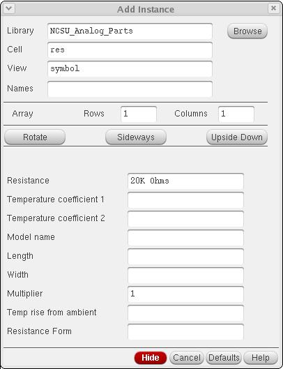
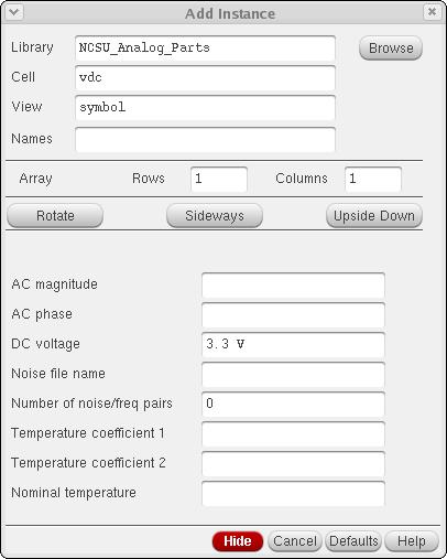
9 Add Components (1/3) All basic components are in the library, NCSU_Analog_Parts There are several groups as shown below: Group Name P_Transistors N_Transistors R_L_C Supply_Nets Voltage_Sources Current_Sources components pmos4 nmos4 res, cap, vdd, gnd vdc,vsin, idc, 9
10 Add Components (2/3) Implement a schematic using the following parameters Resistance: 4KOhm NMOS: W=60um, L=1.2um Input voltage: DC = 770mV, AC = 1V, phase = 0/180 Supply voltage: DC = 3.3V Use wire to connect all components 10
11 Add Components (3/3) 11

12 Add Pins 4 1 Pin Names INN INP OUTN OUTP Direction input input output output 2 3 4) Save & Check Error If there is no error or warning, you implement the schematic successfully. 12
13 Useful Commands & Keyboard Shortcuts Edit Delete Rotate Move Stretch Properties -> Objects ESC Cancel command Add component: i Add wire label: l Add wire: w Add pin: p Copy: c Check and Save: X Delete: Delete Edit properties: q Fit: f Hierarchy->Descend: E Hierarchy->Return: ^e Move: M Redraw: F6 Redo: U Rotate: r Stretch: m Undo: u Zoom in: z Zoom in by 2: [ Zoom out by 2: ] 13
 Setup -> Design 4) Simulator : spectre 3 5) OK 4 5")
14 Cadence Analog Design Environment 1 1) Launch -> ADE L 2) Virtuoso Analog Design Environment Window pop up 3) Setup -> Design 4) Simulator : spectre 3 5) OK
 3) Select : models.scs 4) Select: C0 1 2 4 3 15")
15 Setup Model Libraries 1) Setup -> Model Libraries 2) Model File (double clicks) 3) Select : models.scs 4) Select: C
 4.")
16 Setup Analyses (1/3) 1) Analyses -> Choose 2) In Choosing Analyses Window 1. Analysis dc 2. DC Analysis Save DC Operating Point 3. Analysis ac (see the next page) 4. AC Analysis -- Sweep Variable : Frequency -- Sweep Range Start-Stop Start: 1K Stop: 1G -- Sweep Type Logarithmic -- Select : Point Per Decade OK 16

17 Setup Analyses (2/3) 17

18 Setup Analyses (3/3) After choosing analyses, you could see the dc & ac analyses setting and enable in Virtuoso Analog Design Environment Window 18
 -- OK select :")
19 Setup Outputs 1) Outputs -> Save All 2) In Save Options Window -- Select signals to output (save) -- OK select : all 19
20 Run Simulation & Check Results 1) Simulation -> Netlist and Run 2) Results -> Annotate -> DC Node Voltage 3) Results -> Annotate -> DC Operating Points 4) Check your schematic & See what s changed 5) Tools -> Calculator 20
 Select the net OUTP 5) See what happen in your Calculator Window")
21 Plot the output results (1/3) 1) Select ac 2) Select vf 3) Move your mouse to the schematic Window 4) Select the net OUTP 5) See what happen in your Calculator Window 21
-VF( /OUTN ) 2) Select --db20 3) Select -- plot 1 3 2")
22 Plot the output results (2/3) 1) Fill out VF( /OUTP )-VF( /OUTN ) 2) Select --db20 3) Select -- plot
 Find the 3dB Frequency")
23 Plot the output results (3/3) 1) Check the Frequency Response in Graph Window 2) Find the 3dB Frequency 23
 Delete")
 Save & Check 3) Create -> Cellview ->")

24 Build the symbol from the schematic In Virtuoso Schematic Editor Window 1) Delete the input voltages and the supply voltage 2) Save & Check 3) Create -> Cellview -> From Cellview 4) Click : OK in Cellview From Cellview and Symbol Generation Options Windows 24
25 1) After you implement this simple differential amplifier, you should understand: Building a schematic Simulating a design Checking the simulation results Creating a symbol from the schematic 2) You don t need to write a report for this Lab. However, you need to tell the TA after you have done this example. 3) After the TA checks your results, you are finished with this lab. 25
Cadence Schematic Tutorial. EEE5320/EEE4306 Fall 2015 University of Florida ECE
 Cadence Schematic Tutorial EEE5320/EEE4306 Fall 2015 University of Florida ECE 1 Remote access You may access the Linux server directly from the NEB Computer Lab using your GatorLink username and password.
Virtuoso Schematic Composer
 is a schematic design tool from Cadence. In this tutorial you will learn how to put electrical components, make wire connections, insert pins and check for connection error. Start Cadence Custom IC Design
Revision Notes: July2004 Generate tutorial for single transistor analysis. Based on existing schematic entry tutorial developed for ECE410
 Cadence Analog Tutorial 1: Schematic Entry and Transistor Characterization Created for the MSU VLSI program by Professor A. Mason and the AMSaC lab group. Revision Notes: July2004 Generate tutorial for
CADENCE SETUP. ECE4430-Analog IC Design
 CADENCE SETUP This short tutorial shows how to configure Cadence to use the NCSU Cadence Design Kit (CDK) with access to the ON Semiconductor C5 0.5-µm and the TSMC 0.35-µm CMOS processes libraries. In
Cadence Tutorial: Schematic Entry and Circuit Simulation of a CMOS Inverter
 Cadence Tutorial: Schematic Entry and Circuit Simulation of a CMOS Inverter Introduction This tutorial describes the steps involved in the design and simulation of a CMOS inverter using the Cadence Virtuoso
EECE 285 VLSI Design. Cadence Tutorial EECE 285 VLSI. By: Kevin Dick Co-author: Jeff Kauppila Co-author: Dr. Arthur Witulski
 Cadence Tutorial EECE 285 VLSI By: Kevin Dick Co-author: Jeff Kauppila Co-author: Dr. Arthur Witulski 1 Table of Contents Purpose of Cadence 1) The Purpose of Cadence pg. 4 Linux 1) The Purpose of Linux
ECE471/571 Energy Ecient VLSI Design
 ECE471/571 Energy Ecient VLSI Design Project 2 Cadence Setup and Creation of an Inverter Due Date 11:30pm on Friday, January 30 th 2015 Introduction This project will rst walk you through the setup for
CPE/EE 427, CPE 527, VLSI Design I: Tutorial #2, Schematic Capture, DC Analysis, Transient Analysis (Inverter, NAND2)
") CPE/EE 427, CPE 527, VLSI Design I: Tutorial #2, Schematic Capture, DC Analysis, Transient Analysis (Inverter, NAND2) Joel Wilder, Aleksandar Milenkovic, ECE Dept., The University of Alabama in Huntsville
CPE/EE 427, CPE 527, VLSI Design I: Tutorial #2, Schematic Capture, DC Analysis, Transient Analysis (Inverter, NAND2) Joel Wilder, Aleksandar Milenkovic, ECE Dept., The University of Alabama in Huntsville
Cadence Tutorial A: Schematic Entry and Functional Simulation Created for the MSU VLSI program by Andrew Mason and the AMSaC lab group.
 Cadence Tutorial A: Schematic Entry and Functional Simulation Created for the MSU VLSI program by Andrew Mason and the AMSaC lab group. Revision Notes: Aug. 2003 update and edit A. Mason add intro/revision/contents
Using Cadence Virtuoso, a UNIX based OrCAD PSpice like program, Remotely on a Windows Machine
 Using Cadence Virtuoso, a UNIX based OrCAD PSpice like program, Remotely on a Windows Machine A. Launch PuTTY. 1. Load the Saved Session that has Enable X11 forwarding and the Host Name is cvl.ece.vt.edu.
Intro to Cadence. Brady Salz. ECE483 Spring 17
 Intro to Cadence Brady Salz ECE483 Spring 17 What We re Doing Learn you a Cadence Learn simulation vocabulary Basic schematic guidelines Simulation results Init Before we begin, open a terminal: $ module
Cadence Tutorial. Introduction to Cadence 0.18um, Implementation and Simulation of an inverter. A. Moradi, A. Miled et M. Sawan
 Cadence Tutorial Introduction to Cadence 0.18um, Implementation and Simulation of an inverter A. Moradi, A. Miled et M. Sawan Section 1: Introduction to Cadence You will see how to create a new library
Cadence Analog Circuit Tutorial
 Cadence Analog Circuit Tutorial Schematic Entry for Analog Designs- Passive Circuits (RLC Circuit) In this tutorial, we will build the circuit shown in figure 1 below, using the Cadence Composer tool.
VLSI Lab Tutorial 1. Cadence Virtuoso Schematic Composer Introduction
 VLSI Lab Tutorial 1 Cadence Virtuoso Schematic Composer Introduction 1.0 Introduction The purpose of the first lab tutorial is to help you become familiar with the schematic editor, Virtuoso Schematic
CS755 CAD TOOL TUTORIAL
 CS755 CAD TOOL TUTORIAL CREATING SCHEMATIC IN CADENCE Shi-Ting Zhou shi-ting@cs.wisc.edu After you have figured out what you want to design, and drafted some pictures and diagrams, it s time to input schematics
ECE 331: Electronics Principles I Fall 2014
 ECE 331: Electronics Principles I Fall 2014 Lab #0: Introduction to Computer Modeling and Laboratory Measurements Report due at your registered lab period on the week of Sept. 8-12 Week 1 Accessing Linux
Select the technology library: NCSU_TechLib_ami06, then press OK.
 ECE 126 Inverter Tutorial: Schematic & Symbol Creation Created for GWU by Anis Nurashikin Nordin & Thomas Farmer Tutorial adapted from: http://www.ee.ttu.edu/ee/cadence/commondirectory/final%20tutorials/digitalcircuitsimulationusingvirtuoso.doc
CS/EE 5720/6720 Analog IC Design Tutorial for Schematic Design and Analysis using Spectre
 CS/EE 5720/6720 Analog IC Design Tutorial for Schematic Design and Analysis using Spectre Introduction to Cadence EDA: The Cadence toolset is a complete microchip EDA (Electronic Design Automation) system,
Tutorial on getting started in Cadence. Advanced Analog Circuits Spring 2015 Instructor: Prof. Harish Krishnaswamy TA: Jahnavi Sharma
 Tutorial on getting started in Cadence Advanced Analog Circuits Spring 2015 Instructor: Prof. Harish Krishnaswamy TA: Jahnavi Sharma Getting Started Start Cadence from the terminal by using the command
Virtuoso Layout Editor
 This tutorial will cover the basic steps involved in using the Cadence layout editor called Virtuoso, extracting layout, and running simulation on the layout. The inverter layout is used as an example
Cadence Tutorial A: Schematic Entry and Functional Simulation Created for the MSU VLSI program by Professor A. Mason and the AMSaC lab group.
 Cadence Tutorial A: Schematic Entry and Functional Simulation Created for the MSU VLSI program by Professor A. Mason and the AMSaC lab group. Revision Notes: Jan. 2006 Updated for use with spectre simulator
EE115C Digital Electronic Circuits. Tutorial 2: Hierarchical Schematic and Simulation
 EE115C Digital Electronic Circuits Tutorial 2: Hierarchical Schematic and Simulation The objectives are to become familiar with Virtuoso schematic editor, learn how to create the symbol view of basic primitives,
EE 330 Spring 2018 Laboratory 2: Basic Boolean Circuits
 EE 330 Spring 2018 Laboratory 2: Basic Boolean Circuits Contents Objective:... 2 Part 1: Introduction... 2 Part 2 Simulation of a CMOS Inverter... 3 Part 2.1 Attaching technology information... 3 Part
Figure 1: ADE Test Editor
 Due to some issues that ADE GXL simulation environment has (probably because of inappropriate setup), we will run simulations in the ADE L design environment, which includes all the necessary tools that
Amplifier Simulation Tutorial. Design Kit: Cadence 0.18μm CMOS PDK (gpdk180) (Cadence Version 6.1.5)
 (Cadence Version 6.1.5)") Amplifier Simulation Tutorial Design Kit: Cadence 0.18μm CMOS PDK (gpdk180) (Cadence Version 6.1.5) Yongsuk Choi, Marvin Onabajo This tutorial provides a quick introduction to the use of Cadence tools
Amplifier Simulation Tutorial Design Kit: Cadence 0.18μm CMOS PDK (gpdk180) (Cadence Version 6.1.5) Yongsuk Choi, Marvin Onabajo This tutorial provides a quick introduction to the use of Cadence tools
Lab 1: Cadence Custom IC design tools- Setup, Schematic capture and simulation
 Lab 1: Cadence Custom IC design tools- Setup, Schematic capture and simulation Brittany Duffy EE 330- Integrated Electronics Lab Section B Professor Randy Geiger 1/24/13 Introduction The main goal of this
Experiment 0: Introduction to Cadence
 UNIVERSITY OF CALIFORNIA AT BERKELEY College of Engineering Department of Electrical Engineering and Computer Sciences EE105 Lab Experiments Experiment 0: Introduction to Cadence Contents 1. Introduction...
DOWNLOAD PDF CADENCE WAVEFORM CALCULATOR USER GUIDE
 Chapter 1 : CSE / Cadence Tutorial The Cadence Design Communities support Cadence users and technologists interacting to exchange ideas, news, technical information, and best practices to solve problems
The original document link is
 Tutorial:Analog Artist with HSPICE The original document link is http://www.eda.ncsu.edu/wiki/tutorial:analog_artist_with_hspice This tutorial will introduce you to the Cadence Environment: specifically
ESE570 Spring University of Pennsylvania Department of Electrical and System Engineering Digital Integrated Cicruits AND VLSI Fundamentals
 University of Pennsylvania Department of Electrical and System Engineering Digital Integrated Cicruits AND VLSI Fundamentals ESE570, Spring 2019 HW5: Delay and Layout Sunday, February 17th Due: Friday,
DC Circuit Simulation
 Chapter 2 DC Circuit Simulation 2.1 Starting the Project Manager 1. Select Project Manager from the Start All Program Cadence Release 16.5 Project Manager. 2. Select Allegro PCB Designer (Schematic) from
Introduction to laboratory exercises in Digital IC Design.
 Introduction to laboratory exercises in Digital IC Design. A digital ASIC typically consists of four parts: Controller, datapath, memory, and I/O. The digital ASIC below, which is an FFT/IFFT co-processor,
Laboratory 3. EE 342 (VLSI Circuit Design) - Using Spectre netlist and Calculator for simulation
 - Using Spectre netlist and Calculator for simulation") EE 342 (VLSI Circuit Design) Laboratory 3 - Using Spectre netlist and Calculator for simulation By Mulong Li, 2013 1 Background knowledge Spectre: is a SPICE-class circuit simulator. It provides the basic
EE 342 (VLSI Circuit Design) Laboratory 3 - Using Spectre netlist and Calculator for simulation By Mulong Li, 2013 1 Background knowledge Spectre: is a SPICE-class circuit simulator. It provides the basic
UNIVERSITY OF WATERLOO
 UNIVERSITY OF WATERLOO UW ASIC DESIGN TEAM: Cadence Tutorial Description: Part I: Layout & DRC of a CMOS inverter. Part II: Extraction & LVS of a CMOS inverter. Part III: Post-Layout Simulation. The Cadence
Microelectronica. Full-Custom Design with Cadence Tutorial
 Área Científica de Electrónica Microelectronica Full-Custom Design with Cadence Tutorial AustriaMicroSystems C35B3 (HIT-Kit 3.70) Marcelino Santos Table of contends 1. Starting Cadence... 3 Starting Cadence
Cadence Tutorial D: Using Design Variables and Parametric Analysis Document Contents Introduction Using Design Variables Apply Apply
 Cadence Tutorial D: Using Design Variables and Parametric Analysis Created for the MSU VLSI program by Casey Wallace Last Updated by: Patrick O Hara SS15 Document Contents Introduction Using Design Variables
AMS 0.18 µm PDK Setup and Cadence Tutorial Contributors
 AMS 0.18 µm PDK Setup and Cadence Tutorial Contributors Muhammad Ahmed, Sita Asar, and Ayman Fayed, Power Management Research Lab, https://pmrl.osu.edu, Department of Electrical and Computer Engineering,
Professor Muller Fall 2016 Sameet Ramakrishnan Eric Chang Adapted from prior EE140 and EE141 labs. EE 140/240A Lab 0 Full IC Design Flow
 Professor Muller Fall 2016 Sameet Ramakrishnan Eric Chang Adapted from prior EE140 and EE141 labs EE 140/240A Lab 0 Full IC Design Flow In this lab, you will walk through the full process an analog designer
Cadence Virtuoso Simulation of a pixel
 MEMS AND MICROSENSORS 2018/2019 Cadence Virtuoso Simulation of a pixel 11/12/2018 Giorgio Mussi giorgio.mussi@polimi.it Introduction In this lab, we will use Cadence Virtuoso to simulate a sub-array of
This is a brief tutorial about building a Symbol for a Schematic in Cadence IC design tool environment for hierarchical design of schematics.
 This is a brief tutorial about building a Symbol for a Schematic in Cadence IC design tool environment for hierarchical design of schematics. 1. > cd work035 2. > cadsetup ams035 3. > virtuoso& IMPORTANT:
S Exercise 1C Testing the Ring Oscillator
 S-87.3148 Exercise 1C Testing the Ring Oscillator Aalto University School of Electrical Engineering Department of Micro- and Nanosciences (ECDL) 10.9.2014 1 1 Building the test bench In this exercise,
Cadence Virtuoso Schematic Design and Circuit Simulation Tutorial
 Cadence Virtuoso Schematic Design and Circuit Simulation Tutorial Introduction This tutorial is an introduction to schematic capture and circuit simulation for ENGN1600 using Cadence Virtuoso. These courses
Basic Analog Simulation in Cadence
 York University Department of Electrical Engineering and Computer Science EMIL Tutorial Series Tutorial #1 Basic Analog Simulation in Cadence In this tutorial we step through how to start Cadence (or at
Lab 2: Functional Simulation Using. Affirma Analog Simulator
 Lab 2: Functional Simulation Using Affirma Analog Simulator This Lab will go over: 1. Creating a test bench 2. Simulation in Spectre Spice using the Analog Design environment 1. Creating a test bench:
CPE/EE 427, CPE 527, VLSI Design I: Tutorial #1, Full Custom VLSI (inverter layout)
") CPE/EE 427, CPE 527, VLSI Design I: Tutorial #1, Full Custom VLSI (inverter layout) Joel Wilder, Aleksandar Milenkovic, ECE Dept., The University of Alabama in Huntsville Adapted from Virginia Tech, Dept.
CPE/EE 427, CPE 527, VLSI Design I: Tutorial #1, Full Custom VLSI (inverter layout) Joel Wilder, Aleksandar Milenkovic, ECE Dept., The University of Alabama in Huntsville Adapted from Virginia Tech, Dept.
Cadence Tutorial C: Simulating DC and Timing Characteristics 1
 Cadence Tutorial C: Simulating DC and Timing Characteristics Created for the MSU VLSI program by Professor A. Mason and the AMSaC lab group Last updated by Patrick O Hara SS15 Document Contents Introduction
EE434 ASIC & Digital Systems. From Layout to SPICE Simulation (Virtuoso, Calibre, HSpice) Spring 2017 Dae Hyun Kim
 Spring 2017 Dae Hyun Kim") EE434 ASIC & Digital Systems From Layout to SPICE Simulation (Virtuoso, Calibre, HSpice) Spring 2017 Dae Hyun Kim daehyun@eecs.wsu.edu 1 Preparation for Lab2 Download the following file into your working
EE434 ASIC & Digital Systems From Layout to SPICE Simulation (Virtuoso, Calibre, HSpice) Spring 2017 Dae Hyun Kim daehyun@eecs.wsu.edu 1 Preparation for Lab2 Download the following file into your working
ECE471/571 Energy Efficient VLSI Design Project 2 Cadence Setup and Creation of an Inverter Due Date 11:30 am on Friday, February 2 nd, 2018
 ECE471/571 Energy Efficient VLSI Design Project 2 Cadence Setup and Creation of an Inverter Due Date 11:30 am on Friday, February 2 nd, 2018 Introduction This project will first walk you through the setup
Design rule illustrations for the AMI C5N process can be found at:
 Cadence Tutorial B: Layout, DRC, Extraction, and LVS Created for the MSU VLSI program by Professor A. Mason and the AMSaC lab group. Revised by C Young & Waqar A Qureshi -FS08 Document Contents Introduction
LTSPICE MANUAL. For Teaching Module EE4415 ZHENG HAUN QUN. December 2016
 LTSPICE MANUAL For Teaching Module EE4415 ZHENG HAUN QUN December 2016 DEPARTMENT OF ELECTRICAL AND COMPUTER ENGINNERING NATIONAL UNIVERSITY OF SINGAPORE Contents 1. Introduction... 2 1.1 Installation...
ECEN 474 Homework #2 Notes
 ECEN 474 Homework #2 Notes February 22, 2018 Due: 3-6-2018, 5:00PM Homeworks will not be received after due. Instructor: Sam Palermo 1. (50 points) Technology Characterization for Design In this problem,
EE 330 Fall 2017 Lab 1: Cadence Custom IC design tools - Setup, Schematic capture and simulation
 EE 330 Fall 2017 Lab 1: Cadence Custom IC design tools - Setup, Schematic capture and simulation Table of Contents Objective... 2 1. Setup... 2 Set Bash Shell for the account... 2 2. Starting Cadence Custom
Cadence IC Design Manual
 Cadence IC Design Manual For EE5518 ZHENG Huan Qun Lin Long Yang Revised on May 2017 Department of Electrical & Computer Engineering National University of Singapore 1 P age Contents 1 INTRODUCTION...
How to Start with Cadence ECE721 Project. Instructor: Prof. Steve Bibyk Prepared by: Golsa Ghiaasi Hafezi Spring 2005 Ohio State University
 How to Start with Cadence ECE721 Project Instructor: Prof. Steve Bibyk Prepared by: Golsa Ghiaasi Hafezi Spring 2005 Ohio State University Follow the instruction for installing AMI05 process posted on
VLSI Lab Tutorial 3. Virtuoso Layout Editing Introduction
 VLSI Lab Tutorial 3 Virtuoso Layout Editing Introduction 1.0 Introduction The purpose of this lab tutorial is to guide you through the design process in creating a custom IC layout for your CMOS inverter
EE 330 Spring 2018 Lab 1: Cadence Custom IC design tools Setup, Schematic capture and simulation
 EE 330 Spring 2018 Lab 1: Cadence Custom IC design tools Setup, Schematic capture and simulation Table of Contents Objective... 2 1. Setup... 2 Set Bash Shell for the account... 2 2. Starting Cadence Custom
ESE 570 Cadence Lab Assignment 2: Introduction to Spectre, Manual Layout Drawing and Post Layout Simulation (PLS)
") ESE 570 Cadence Lab Assignment 2: Introduction to Spectre, Manual Layout Drawing and Post Layout Simulation (PLS) Objective Part A: To become acquainted with Spectre (or HSpice) by simulating an inverter,
ESE 570 Cadence Lab Assignment 2: Introduction to Spectre, Manual Layout Drawing and Post Layout Simulation (PLS) Objective Part A: To become acquainted with Spectre (or HSpice) by simulating an inverter,
Lab 2. Standard Cell layout.
 Lab 2. Standard Cell layout. The purpose of this lab is to demonstrate CMOS-standard cell design. Use the lab instructions and the cadence manual (http://www.es.lth.se/ugradcourses/cadsys/cadence.html)
Click on the SwCAD III shortcut created by the software installation.
 LTSpice Guide Click on the SwCAD III shortcut created by the software installation. Select File and New Schematic. Add a component Add a resistor Press R or click the resistor button to insert a resistor.
Lab 1: An Introduction to Cadence
 GIF-4201/GEL-7016 (Micro-électronique) Lab 1: An Introduction to Cadence Schematic, simulation and layout Gabriel Gagnon-Turcotte, Mehdi Noormohammadi Khiarak and Benoit Gosselin Department of Electrical
MENTOR GRAPHICS IC DESIGN MANUAL. Schematic & Simulation. Gun Jun K Praveen Jayakar Thomas Zheng Huan Qun
 MENTOR GRAPHICS IC DESIGN MANUAL Schematic & Simulation By Gun Jun K Praveen Jayakar Thomas Zheng Huan Qun August 2004 Signal Processing & VLSI Design Laboratory Department of Electrical & Computer Engineering
Introduction to Design Architect
 SANTA CLARA UNIVERSITY Dept. of Electrical Engineering Mentor Graphics Tutorials Introduction to Design Architect Yiching Chen Sangeetha Raman S. Krishnan I. Introduction II. This document contains a step-by-step
Fall 2008: EE5323 VLSI Design I using Cadence
 1 of 23 9/17/2008 6:47 PM Fall 2008: EE5323 VLSI Design I using Cadence This tutorial has been adapted from EE5323 offered in Fall 2007. Thanks to Jie Gu, Prof. Chris Kim and Satish Sivaswamy of the University
EE115C Digital Electronic Circuits. Tutorial 4: Schematic-driven Layout (Virtuoso XL)
") EE115C Digital Electronic Circuits Tutorial 4: Schematic-driven Layout (Virtuoso XL) This tutorial will demonstrate schematic-driven layout on the example of a 2-input NAND gate. Simple Layout (that won
EE115C Digital Electronic Circuits Tutorial 4: Schematic-driven Layout (Virtuoso XL) This tutorial will demonstrate schematic-driven layout on the example of a 2-input NAND gate. Simple Layout (that won
EE 471: Transport Phenomena in Solid State Devices
 EE 471: Transport Phenomena in Solid State Devices HW7 Due: 4/17/18 For this homework, you will download a free PC version of the industry standard SPICE circuit simulator called LTspice, provided by Linear
EEC 116 Fall 2011 Lab #1 Cadence Schematic Capture and Layout Tutorial
 EEC 116 Fall 2011 Lab #1 Cadence Schematic Capture and Layout Tutorial Dept. of Electrical and Computer Engineering University of California, Davis September 26, 2011 Reading: Rabaey Chapters 1, 2, A,
ANALOG MICROELECTRONICS ( A)
") ANALOG MICROELECTRONICS (304-534A) IBM 130 nm CMOS Technology An Introduction to Cadence Virtuoso Layout Tool and the Analog Simulation Environment Prepared By - Azhar A. Chowdhury Updated by Ming Yang
ANALOG MICROELECTRONICS (304-534A) IBM 130 nm CMOS Technology An Introduction to Cadence Virtuoso Layout Tool and the Analog Simulation Environment Prepared By - Azhar A. Chowdhury Updated by Ming Yang
Guide to the CSE 577 Lab and Cad tools
 Guide to the CSE 577 Lab and Cad tools 1. Introduction The objective of this tutorial is to give you an overview to (1) setup the Cadence and Synopsys hspice tools for your account in IST 218 Lab, (2)
EE 330 Laboratory 3 Layout, DRC, and LVS Fall 2015
 EE 330 Laboratory 3 Layout, DRC, and LVS Fall 2015 Contents Objective:... 2 Part 1 Creating a layout... 2 1.1 Run DRC Early and Often... 2 1.2 Create N active and connect the transistors... 3 1.3 Vias...
Tutorial II: Cadence Virtuoso ECE6133: Physical Design Automation of VLSI Systems Georgia Institute of Technology Prof.
 Tutorial II: Cadence Virtuoso ECE6133: Physical Design Automation of VLSI Systems Georgia Institute of Technology Prof. Sung Kyu Lim I. Setup for Cadence Virtuoso 1. Copy the following files into your
Mentor Graphics VLSI CAD Tutorials
 VLSI Design Flow Using Mentor-Graphics Tools Mentor Graphics VLSI CAD Tutorials School of Engineering Santa Clara University Santa Clara, CA 95053 At the Design Center, School of Engineering, of Santa
EECS 211 CAD Tutorial. 1. Introduction
 EECS 211 CAD Tutorial 1. Introduction This tutorial has been devised to run through all the steps involved in the design and simulation of an audio tone control amplifier using the Mentor Graphics CAD
Logging in, starting a shell tool, and starting the Cadence Tool Suite
 EEE 4134 VLSI I Laboratory Lab 0 (Introductory Lab) Logging into Cadence Server, Tool Setup, Cell Library Creation, Introduction to Custom IC Design flow Objectives: To login, start a shell tool and start
EE 330 Laboratory 3 Layout, DRC, and LVS
 EE 330 Laboratory 3 Layout, DRC, and LVS Spring 2018 Contents Objective:... 2 Part 1 creating a layout... 2 1.1 Run DRC... 2 1.2 Stick Diagram to Physical Layer... 3 1.3 Bulk Connections... 3 1.4 Pins...
The Design and Simulation of an Inverter
 The Design and Simulation of an Inverter Cadence Tutorial This tutorial has been devised to run through all the steps involved in the design and simulation of a CMOS inverter using the Cadence CAD tools.
More information can be found in the Cadence manuals Virtuoso Layout Editor User Guide and Cadence Hierarchy Editor User Guide.
 Chapter 6 Building with Layout This chapter consists of two parts. The first describes the generation of layout views and the second deals with the various tools used for verifying the layout, both physical
EE 140/240A - Full IC Design Flow Tutorial
 Original document by Filip Maksimovic & Mike Lorek, Spring 2015, derived from earlier EE141 lab manuals Revisions for IC6 by David Burnett & Thaibao Phan, Spring 2016 Revisions made by Nandish Mehta to
Simulation examples Chapter overview
 Simulation examples 2 Chapter overview The examples in this chapter provide an introduction to the methods and tools for creating circuit designs, running simulations, and analyzing simulation results.
TUTORIAL II ECE 555 / 755 Updated on September 11 th 2006 CADENCE LAYOUT AND PARASITIC EXTRACTION
 TUTORIAL II ECE 555 / 755 Updated on September 11 th 2006 CADENCE LAYOUT AND PARASITIC EXTRACTION After finishing a schematic of your design (Tutorial-I), the next step is creating masks which are for
DRC and LVS checks using Cadence Virtuoso Version 2.0
 DRC and LVS checks using Cadence Virtuoso Version 2.0 Start virtuoso l l Open a virtuoso session in the directory which contains the required cds.lib and lib.def files. Command : virtuoso & Open the layout
Virtuoso Schematic Composer VHDL Interface. VHDL In for Design Framework II:
 Virtuoso Schematic Composer VHDL Interface. VHDL In for Design Framework II: VHDL In for Design Framework II can convert a VHDL structural or behavioral description into one of three forms in Cadence database
DRC and LVS checks using Cadence Virtuoso Version 3.0
 DRC and LVS checks using Cadence Virtuoso Version 3.0 Start virtuoso l l Open a virtuoso session in the directory which contains the required cds.lib and lib.def files. Command : virtuoso & Open the layout
EE 330 Spring Laboratory 2: Basic Boolean Circuits
 EE 330 Spring 2013 Laboratory 2: Basic Boolean Circuits Objective: The objective of this experiment is to investigate methods for evaluating the performance of Boolean circuits. Emphasis will be placed
CMOS Design Lab Manual
 CMOS Design Lab Manual Developed By University Program Team CoreEl Technologies (I) Pvt. Ltd. 1 Objective Objective of this lab is to learn the Mentor Graphics HEP2 tools as well learn the flow of the
Introduction to CCV and Cadence Virtuoso for Electronic Circuit Simulation
 Introduction to CCV and Cadence Virtuoso for Electronic Circuit Simulation Introduction ENGN1600 will be using the Cadence Virtuoso software suite for its circuit design and SPICE components. Part of the
Setting up an initial ".tcshrc" file
 ECE445 Fall 2005 Introduction to SaberSketch The SABER simulator is a tool for computer simulation of analog systems, digital systems and mixed signal systems. SaberDesigner consists of the three tools,
Getting started. Starting Capture. To start Capture. This chapter describes how to start OrCAD Capture.
 Getting started 1 This chapter describes how to start OrCAD Capture. Starting Capture The OrCAD Release 9 installation process puts Capture in the \PROGRAM FILES\ORCAD\CAPTURE folder, and adds Pspice Student
ELEC451 Integrated Circuit Engineering Using Cadence's Virtuoso Layout Editing Tool
 ELEC451 Integrated Circuit Engineering Using Cadence's Virtuoso Layout Editing Tool Contents Contents 1. General 2. Creating and Working On a Layout o 2.1 Undoing/Re-doing an Action o 2.2 Display Options
ECE 425: Introduction to VLSI System Design Machine Problem 0 Due: Friday 11:59pm, Sep. 15th, 2017
 ECE 425: Introduction to VLSI System Design Machine Problem 0 Due: Friday 11:59pm, Sep. 15th, 2017 You will spend most of your lab time using the Virtuoso design tools from Cadence Design Systems. Virtuoso
OrCad & Spice Tutorial By, Ronak Gandhi Syracuse University
 OrCad & Spice Tutorial By, Ronak Gandhi Syracuse University Brief overview: OrCad is a suite of tools from Cadence for the design and layout of circuit design and PCB design. We are currently using version
Creating LEF File. Abstract Generation: Creating LEF Tutorial File Release Date: 01/13/2004. Export GDS:
 Creating LEF Tutorial 1-1 - Creating LEF File Abstract Generation: Export GDS: Abstract generator comes as a part of the Silicon Ensemble package. As such, it cannot directly read ICFB library databases.
EE5323/5324 VLSI Design I/II using Cadence
 1 of 18 2009-1-23 23:58 Spring 2009: EE5323/5324 VLSI Design I/II using Cadence This tutorial has been adapted from EE5323 offered in Fall 2007. Thanks to Jie Gu, Prof. Chris Kim and Satish Sivaswamy of
ELEC 301 Lab 2: Cadence Basic
 ELEC 301 Lab 2: Cadence Basic Revision: 2.1 Last modified: Aug. 98 Introduction In this class, you will be introduced to the Cadence suit of IC design tools. These tools are a very powerful set of tools.
How to Get Started. Figure 3
 Tutorial PSpice How to Get Started To start a simulation, begin by going to the Start button on the Windows toolbar, then select Engineering Tools, then OrCAD Demo. From now on the document menu selection
Cadence Tutorial 2: Layout, DRC/LVS and Circuit Simulation with Extracted Parasitics
 Cadence Tutorial 2: Layout, DRC/LVS and Circuit Simulation with Extracted Parasitics Introduction This tutorial describes how to generate a mask layout in the Cadence Virtuoso Layout Editor. Use of DIVA
The following is a procedure for extracting a layout, doing a layout vs. schematic check, and then simulating the extracted layout with Cadence.
 The following is a procedure for extracting a layout, doing a layout vs. schematic check, and then simulating the extracted layout with Cadence. (This might not be the best way, but it works!) 1) Realize
Lesson 19: Processing a Hierarchical Design
 Lesson 19: Processing a Hierarchical Design Lesson Objectives After you complete this lesson you will be able to: Annotate a hierarchical design Perform a Design Rule Check on a hierarchical design Correct
Beginners manual for Cadence
 Starting the Cadence for the first time. Beginners manual for Cadence Drawing 1: Cadence initialization (terminal window) Follow these steps [Drawing 1]: create new subdirectory ( use 'mkdir' command for
PSpice Tutorial. Physics 160 Spring 2006
 PSpice Tutorial This is a tutorial designed to guide you through the simulation assignment included in the first homework set. You may either use the program as installed in the lab, or you may install
FACULTY OF ENGINEERING MULTIMEDIA UNIVERSITY LAB SHEET DIGITAL INTEGRATED CIRCUIT
 FACULTY OF ENGINEERING MULTIMEDIA UNIVERSITY LAB SHEET DIGITAL INTEGRATED CIRCUIT DIC1: Schematic Design Entry, Simulation & Verification DIC2: Schematic Driven Layout Drawing (SDL) Design Rule Check (DRC)