DRC and LVS checks using Cadence Virtuoso Version 2.0
|
|
|
- Lucas Scott
- 5 years ago
- Views:
Transcription
1 DRC and LVS checks using Cadence Virtuoso Version 2.0

2 Start virtuoso l l Open a virtuoso session in the directory which contains the required cds.lib and lib.def files. Command : virtuoso &
3 Open the layout corresponding to your design(final_chip) in layout XL by right clicking on the layout and selecting open with. Change the application to layout XL. This will open the schematic as well as the layout. For DRC check go to verify -> DRC. Specify the rules file and uncheck the Rules library. Result will be displayed in the virtuoso command window
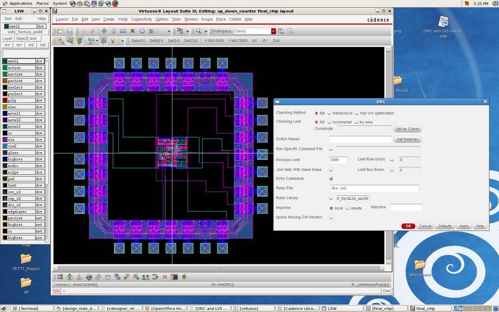
4
5
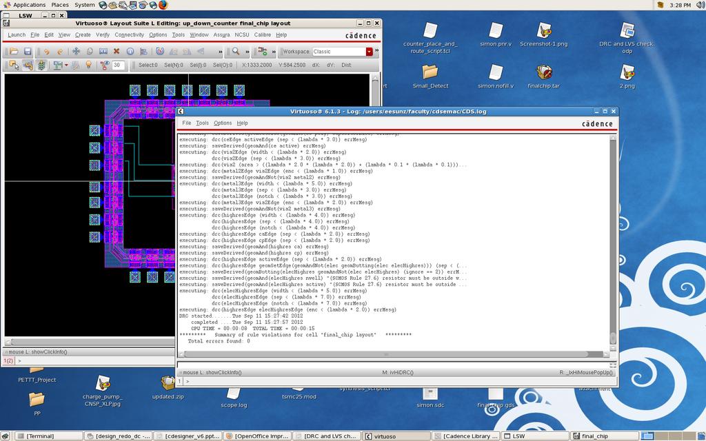
6 Make sure that the total errors are zero. If errors are found fix the errors before proceeding to the next steps. You can use the errors displayed in the command window to debug or also use the following to zoom into the errors locations : verify->markers->find. Select zoom to markers and then cycle through the different errors by hitting Next. Uncheck the warnings to display only the errors during this process.
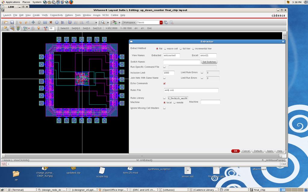
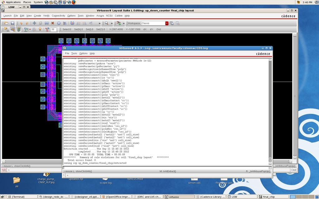
7 Extracting the design for LVS check: Go to verify-> extract Specify the rules file and uncheck the rules library. The results will be displayed in the command window. A successful extraction(total errors = 0) will generate a extracted cell view. Verify this using the library manager.
8
9
10
11 LVS check: LVS will compare the extracted and the schematic views. Go to verify->lvs. Select Form contents and click ok if a Artist LVS form contents Form contents Different window pops up. Specify the schematic and extracted views for your design. Specify the rules file and Hit run.
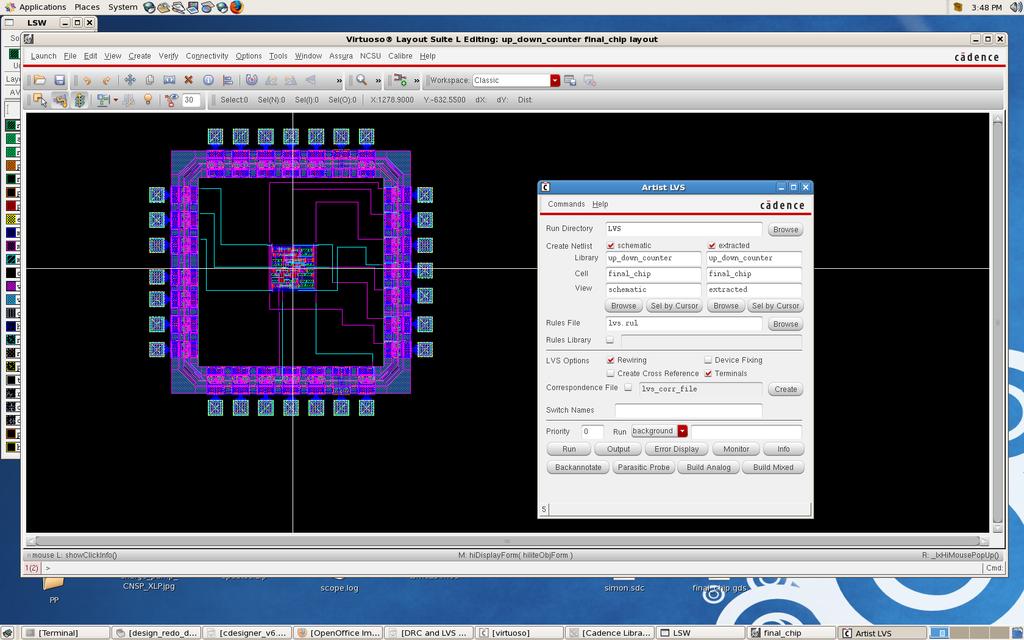
12
13
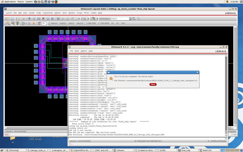
14 Make sure that the design passes LVS. The previous slide shows the output generated when the design passes LVS. IF the netlists don't match use the following resources to correct your layout or schematic: -> click on output in the Artist LVS window to get the report that will show the errors in more detail. -> You can also use the info button in the Artist LVS window to get a more detailed view of the errors for schematic or layout separately.
15 -> You can also use the Error Display button in the artist LVS window to cycle through the different errors in the extracted view and then correct them in the layout view. Make sure to open the extracted view before doing this procedure. The schematic can then be opened to cycle through the errors there too. -> Also the shorts locator can be used to find any net locations causing trouble in the extracted view.
16 Following are some rules that can help you debug the design using the output from the Artist LVS window: Number of terminals don't match: This is commonly due to missing terminals/pins in the layout or mismatch in terminal names between layout and schematic. Number of nets don't match: If the number of nets given for your layout is higher than that of schematic then layout is missing some connections.
17 The first scenario for this situation is that your output will say something like?net /net 027 merged with / R. What the above line means is that net 027, which is some internal connection in the circuit, needs to be connected to terminal R. The second scenario for this situation is that your output will say something like terminal gnd! in layout fails to match any terminal in the schematic. In the given case,a transistor that should be connected to gnd! probably is not connected, so you would need to inspect your layout and find where a connection needs to be made. If the number of nets in the layout is less than that of the schematic then there are some connections in the layout that need not be made but are present.
18 Note : In case the LVS process terminates in the middle giving the following error: The LVS job failed to run to completion click on info button in the artist LVS window and open the log file and check the schematics that need a check and save(towards the bottom of the log file you will see something like xyz has been changed since last extracted). Check the save the required schematics and then re run LVS.
DRC and LVS checks using Cadence Virtuoso Version 3.0
 DRC and LVS checks using Cadence Virtuoso Version 3.0 Start virtuoso l l Open a virtuoso session in the directory which contains the required cds.lib and lib.def files. Command : virtuoso & Open the layout
The following is a procedure for extracting a layout, doing a layout vs. schematic check, and then simulating the extracted layout with Cadence.
 The following is a procedure for extracting a layout, doing a layout vs. schematic check, and then simulating the extracted layout with Cadence. (This might not be the best way, but it works!) 1) Realize
CADENCE SETUP. ECE4430-Analog IC Design
 CADENCE SETUP This short tutorial shows how to configure Cadence to use the NCSU Cadence Design Kit (CDK) with access to the ON Semiconductor C5 0.5-µm and the TSMC 0.35-µm CMOS processes libraries. In
Creating Verilog Tutorial Netlist Release Date: 01/13/2005(Version 2)
") Creating Verilog Tutorial 2-1 - Creating a verilog netlist for a schematic: The verilog netlist is necessary for automatic layout (placement and routing) tools. It contains information about the I/O pins
Creating Verilog Tutorial 2-1 - Creating a verilog netlist for a schematic: The verilog netlist is necessary for automatic layout (placement and routing) tools. It contains information about the I/O pins
Virtuoso Schematic Composer
 is a schematic design tool from Cadence. In this tutorial you will learn how to put electrical components, make wire connections, insert pins and check for connection error. Start Cadence Custom IC Design
HOMEWORK 9 CMPEN 411 Due: 4/12/ :30pm
 HOMEWORK 9 CMPEN 411 Due: 4/12/2016 11:30pm Learning Objective Complete the full 8 bit RISC microprocessor chip design by placing the processor core design into the 40 pin 'tiny' chip pad frame. Do verify
Tutorial II: Cadence Virtuoso ECE6133: Physical Design Automation of VLSI Systems Georgia Institute of Technology Prof.
 Tutorial II: Cadence Virtuoso ECE6133: Physical Design Automation of VLSI Systems Georgia Institute of Technology Prof. Sung Kyu Lim I. Setup for Cadence Virtuoso 1. Copy the following files into your
Virtuoso Layout Editor
 This tutorial will cover the basic steps involved in using the Cadence layout editor called Virtuoso, extracting layout, and running simulation on the layout. The inverter layout is used as an example
Lab 2. Standard Cell layout.
 Lab 2. Standard Cell layout. The purpose of this lab is to demonstrate CMOS-standard cell design. Use the lab instructions and the cadence manual (http://www.es.lth.se/ugradcourses/cadsys/cadence.html)
EE115C Digital Electronic Circuits. Tutorial 4: Schematic-driven Layout (Virtuoso XL)
") EE115C Digital Electronic Circuits Tutorial 4: Schematic-driven Layout (Virtuoso XL) This tutorial will demonstrate schematic-driven layout on the example of a 2-input NAND gate. Simple Layout (that won
EE115C Digital Electronic Circuits Tutorial 4: Schematic-driven Layout (Virtuoso XL) This tutorial will demonstrate schematic-driven layout on the example of a 2-input NAND gate. Simple Layout (that won
EE434 ASIC & Digital Systems. From Layout to SPICE Simulation (Virtuoso, Calibre, HSpice) Spring 2017 Dae Hyun Kim
 Spring 2017 Dae Hyun Kim") EE434 ASIC & Digital Systems From Layout to SPICE Simulation (Virtuoso, Calibre, HSpice) Spring 2017 Dae Hyun Kim daehyun@eecs.wsu.edu 1 Preparation for Lab2 Download the following file into your working
EE434 ASIC & Digital Systems From Layout to SPICE Simulation (Virtuoso, Calibre, HSpice) Spring 2017 Dae Hyun Kim daehyun@eecs.wsu.edu 1 Preparation for Lab2 Download the following file into your working
EDA-BASED DESIGN PRACTICAL LABORATORY SESSION No. 3
 LABORATOIRE DE SYSTEMES MICROELECTRONIQUES EPFL STI IMM LSM ELD Station nº 11 CH-1015 Lausanne Téléphone : Fax : E-mail : Site web : +4121 693 6955 +4121 693 6959 lsm@epfl.ch lsm.epfl.ch EDA-BASED DESIGN
Revision Notes: July2004 Generate tutorial for single transistor analysis. Based on existing schematic entry tutorial developed for ECE410
 Cadence Analog Tutorial 1: Schematic Entry and Transistor Characterization Created for the MSU VLSI program by Professor A. Mason and the AMSaC lab group. Revision Notes: July2004 Generate tutorial for
Lab 4 LVS and Post layout Simulation
 Lab 4 LVS and Post layout Simulation Objective: In this lab you will learn 1. How to check if your layout that you drew in lab 3 matches your schematic that you drew in lab 2. 2. How to do the post layout
Design rule illustrations for the AMI C5N process can be found at:
 Cadence Tutorial B: Layout, DRC, Extraction, and LVS Created for the MSU VLSI program by Professor A. Mason and the AMSaC lab group. Revised by C Young & Waqar A Qureshi -FS08 Document Contents Introduction
Verifying the Multiplexer Layout
 4 This chapter introduces you to interactive verification. You will perform two different tests in the Virtuoso layout editor while using Assura interactive verification products. One test uses the Design
VLSI Lab Tutorial 3. Virtuoso Layout Editing Introduction
 VLSI Lab Tutorial 3 Virtuoso Layout Editing Introduction 1.0 Introduction The purpose of this lab tutorial is to guide you through the design process in creating a custom IC layout for your CMOS inverter
EE 330 Laboratory Experiment Number 11
 EE 330 Laboratory Experiment Number 11 Design and Simulation of Digital Circuits using Hardware Description Languages Fall 2017 Contents Purpose:... 3 Background... 3 Part 1: Inverter... 4 1.1 Simulating
Cadence Schematic Tutorial. EEE5320/EEE4306 Fall 2015 University of Florida ECE
 Cadence Schematic Tutorial EEE5320/EEE4306 Fall 2015 University of Florida ECE 1 Remote access You may access the Linux server directly from the NEB Computer Lab using your GatorLink username and password.
ANALOG MICROELECTRONICS ( A)
") ANALOG MICROELECTRONICS (304-534A) IBM 130 nm CMOS Technology An Introduction to Cadence Virtuoso Layout Tool and the Analog Simulation Environment Prepared By - Azhar A. Chowdhury Updated by Ming Yang
ANALOG MICROELECTRONICS (304-534A) IBM 130 nm CMOS Technology An Introduction to Cadence Virtuoso Layout Tool and the Analog Simulation Environment Prepared By - Azhar A. Chowdhury Updated by Ming Yang
VLSI Lab Tutorial 1. Cadence Virtuoso Schematic Composer Introduction
 VLSI Lab Tutorial 1 Cadence Virtuoso Schematic Composer Introduction 1.0 Introduction The purpose of the first lab tutorial is to help you become familiar with the schematic editor, Virtuoso Schematic
TUTORIAL II ECE 555 / 755 Updated on September 11 th 2006 CADENCE LAYOUT AND PARASITIC EXTRACTION
 TUTORIAL II ECE 555 / 755 Updated on September 11 th 2006 CADENCE LAYOUT AND PARASITIC EXTRACTION After finishing a schematic of your design (Tutorial-I), the next step is creating masks which are for
CMOS VLSI Design Lab 4: Full Chip Assembly
 CMOS VLSI Design Lab 4: Full Chip Assembly In this final lab, you will assemble and simulate your entire MIPS microprocessor! You will build your top level chip cell by connecting the datapath, aludec,
ELEC 301 Lab 2: Cadence Basic
 ELEC 301 Lab 2: Cadence Basic Revision: 2.1 Last modified: Aug. 98 Introduction In this class, you will be introduced to the Cadence suit of IC design tools. These tools are a very powerful set of tools.
More information can be found in the Cadence manuals Virtuoso Layout Editor User Guide and Cadence Hierarchy Editor User Guide.
 Chapter 6 Building with Layout This chapter consists of two parts. The first describes the generation of layout views and the second deals with the various tools used for verifying the layout, both physical
EE 330 Laboratory 3 Layout, DRC, and LVS Fall 2015
 EE 330 Laboratory 3 Layout, DRC, and LVS Fall 2015 Contents Objective:... 2 Part 1 Creating a layout... 2 1.1 Run DRC Early and Often... 2 1.2 Create N active and connect the transistors... 3 1.3 Vias...
Cadence Tutorial A: Schematic Entry and Functional Simulation Created for the MSU VLSI program by Andrew Mason and the AMSaC lab group.
 Cadence Tutorial A: Schematic Entry and Functional Simulation Created for the MSU VLSI program by Andrew Mason and the AMSaC lab group. Revision Notes: Aug. 2003 update and edit A. Mason add intro/revision/contents
ELEC451 Integrated Circuit Engineering Using Cadence's Virtuoso Layout Editing Tool
 ELEC451 Integrated Circuit Engineering Using Cadence's Virtuoso Layout Editing Tool Contents Contents 1. General 2. Creating and Working On a Layout o 2.1 Undoing/Re-doing an Action o 2.2 Display Options
UNIVERSITY OF WATERLOO
 UNIVERSITY OF WATERLOO UW ASIC DESIGN TEAM: Cadence Tutorial Description: Part I: Layout & DRC of a CMOS inverter. Part II: Extraction & LVS of a CMOS inverter. Part III: Post-Layout Simulation. The Cadence
Cadence Tutorial C: Simulating DC and Timing Characteristics 1
 Cadence Tutorial C: Simulating DC and Timing Characteristics Created for the MSU VLSI program by Professor A. Mason and the AMSaC lab group Last updated by Patrick O Hara SS15 Document Contents Introduction
Synopsys Custom Designer Tutorial for a chip integra7on using the University of Utah Standard Cell Libraries In ON Semiconductor 0.
 Synopsys Custom Designer Tutorial for a chip integra7on using the University of Utah Standard Cell Libraries In ON Semiconductor 0.5u C5 CMOS Version 6.0 Overview This tutorial will take you through the
HOMEWORK 10 CMPEN 411 Due: 4/28/ :30pm
 HOMEWORK 10 CMPEN 411 Due: 4/28/2016 11:30pm Instruction First, fabrication ready the full 8 bit RISC microprocessor chip: redesign the chip (its components) to fit the entire chip fitted into the 40 pin
Cadence IC Design Manual
 Cadence IC Design Manual For EE5518 ZHENG Huan Qun Lin Long Yang Revised on May 2017 Department of Electrical & Computer Engineering National University of Singapore 1 P age Contents 1 INTRODUCTION...
Virtuoso Schematic Composer VHDL Interface. VHDL In for Design Framework II:
 Virtuoso Schematic Composer VHDL Interface. VHDL In for Design Framework II: VHDL In for Design Framework II can convert a VHDL structural or behavioral description into one of three forms in Cadence database
Amplifier Simulation Tutorial. Design Kit: Cadence 0.18μm CMOS PDK (gpdk180) (Cadence Version 6.1.5)
 (Cadence Version 6.1.5)") Amplifier Simulation Tutorial Design Kit: Cadence 0.18μm CMOS PDK (gpdk180) (Cadence Version 6.1.5) Yongsuk Choi, Marvin Onabajo This tutorial provides a quick introduction to the use of Cadence tools
Amplifier Simulation Tutorial Design Kit: Cadence 0.18μm CMOS PDK (gpdk180) (Cadence Version 6.1.5) Yongsuk Choi, Marvin Onabajo This tutorial provides a quick introduction to the use of Cadence tools
EECE 285 VLSI Design. Cadence Tutorial EECE 285 VLSI. By: Kevin Dick Co-author: Jeff Kauppila Co-author: Dr. Arthur Witulski
 Cadence Tutorial EECE 285 VLSI By: Kevin Dick Co-author: Jeff Kauppila Co-author: Dr. Arthur Witulski 1 Table of Contents Purpose of Cadence 1) The Purpose of Cadence pg. 4 Linux 1) The Purpose of Linux
Experiment 0: Introduction to Cadence
 UNIVERSITY OF CALIFORNIA AT BERKELEY College of Engineering Department of Electrical Engineering and Computer Sciences EE105 Lab Experiments Experiment 0: Introduction to Cadence Contents 1. Introduction...
DOWNLOAD PDF CADENCE WAVEFORM CALCULATOR USER GUIDE
 Chapter 1 : CSE / Cadence Tutorial The Cadence Design Communities support Cadence users and technologists interacting to exchange ideas, news, technical information, and best practices to solve problems
EE 330 Laboratory 3 Layout, DRC, and LVS
 EE 330 Laboratory 3 Layout, DRC, and LVS Spring 2018 Contents Objective:... 2 Part 1 creating a layout... 2 1.1 Run DRC... 2 1.2 Stick Diagram to Physical Layer... 3 1.3 Bulk Connections... 3 1.4 Pins...
This is a brief tutorial about building a Symbol for a Schematic in Cadence IC design tool environment for hierarchical design of schematics.
 This is a brief tutorial about building a Symbol for a Schematic in Cadence IC design tool environment for hierarchical design of schematics. 1. > cd work035 2. > cadsetup ams035 3. > virtuoso& IMPORTANT:
Abstract Editor (Last updated: Oct. 23, 2008)
") Abstract Editor (Last updated: Oct. 23, 2008) Abstract Editor Tutorial This tutorial has been created to discuss all of the steps needed to create an abstract Library Exchange Format (LEF) file for custom
Abstract Editor (Last updated: Oct. 23, 2008) Abstract Editor Tutorial This tutorial has been created to discuss all of the steps needed to create an abstract Library Exchange Format (LEF) file for custom
ESE 570 Cadence Lab Assignment 2: Introduction to Spectre, Manual Layout Drawing and Post Layout Simulation (PLS)
") ESE 570 Cadence Lab Assignment 2: Introduction to Spectre, Manual Layout Drawing and Post Layout Simulation (PLS) Objective Part A: To become acquainted with Spectre (or HSpice) by simulating an inverter,
ESE 570 Cadence Lab Assignment 2: Introduction to Spectre, Manual Layout Drawing and Post Layout Simulation (PLS) Objective Part A: To become acquainted with Spectre (or HSpice) by simulating an inverter,
ASIC Physical Design Top-Level Chip Layout
 ASIC Physical Design Top-Level Chip Layout References: M. Smith, Application Specific Integrated Circuits, Chap. 16 Cadence Virtuoso User Manual Top-level IC design process Typically done before individual
Fall 2008: EE5323 VLSI Design I using Cadence
 1 of 23 9/17/2008 6:47 PM Fall 2008: EE5323 VLSI Design I using Cadence This tutorial has been adapted from EE5323 offered in Fall 2007. Thanks to Jie Gu, Prof. Chris Kim and Satish Sivaswamy of the University
Setting up the IBM 65nm libraries in Cadence 6.1
 Setting up the IBM 65nm libraries in Cadence 6.1 Preeti Mulage v1 (Jan, 2010) 1. Setting up Cadence 6.1 and Spectre MMSIM 7.1 a. You need to incorporate these lines in order to bring up the latest 6.1
EE4111 Advanced Analog Electronics Design. Spring 2009 Experiment #4 April 6 ~ April 17
 EE4111 Advanced Analog Electronics Design Spring 2009 Experiment #4 April 6 ~ April 17 Setup Cadence in VLSI Lab 1) Copy files $ cp r /home/grads/ee4111ta ~/ 2) Edit your.cshrc file -- Include the following
Orcad Layout Plus Tutorial
 Orcad Layout Plus Tutorial Layout Plus is a circuit board layout tool that accepts a layout-compatible circuit netlist (ex. from Capture CIS) and generates an output layout files that suitable for PCB
How to Start with Cadence ECE721 Project. Instructor: Prof. Steve Bibyk Prepared by: Golsa Ghiaasi Hafezi Spring 2005 Ohio State University
 How to Start with Cadence ECE721 Project Instructor: Prof. Steve Bibyk Prepared by: Golsa Ghiaasi Hafezi Spring 2005 Ohio State University Follow the instruction for installing AMI05 process posted on
The original document link is
 Tutorial:Analog Artist with HSPICE The original document link is http://www.eda.ncsu.edu/wiki/tutorial:analog_artist_with_hspice This tutorial will introduce you to the Cadence Environment: specifically
Microelectronica. Full-Custom Design with Cadence Tutorial
 Área Científica de Electrónica Microelectronica Full-Custom Design with Cadence Tutorial AustriaMicroSystems C35B3 (HIT-Kit 3.70) Marcelino Santos Table of contends 1. Starting Cadence... 3 Starting Cadence
UNIVERSITY OF CALIFORNIA College of Engineering Department of Electrical Engineering and Computer Sciences Lab #2: Layout and Simulation
 UNIVERSITY OF CALIFORNIA College of Engineering Department of Electrical Engineering and Computer Sciences Lab #2: Layout and Simulation NTU IC541CA 1 Assumed Knowledge This lab assumes use of the Electric
CS/EE 5720/6720 Analog IC Design Tutorial for Schematic Design and Analysis using Spectre
 CS/EE 5720/6720 Analog IC Design Tutorial for Schematic Design and Analysis using Spectre Introduction to Cadence EDA: The Cadence toolset is a complete microchip EDA (Electronic Design Automation) system,
Cadence Virtuoso Schematic Design and Circuit Simulation Tutorial
 Cadence Virtuoso Schematic Design and Circuit Simulation Tutorial Introduction This tutorial is an introduction to schematic capture and circuit simulation for ENGN1600 using Cadence Virtuoso. These courses
EECS 627, Lab Assignment 3
 EECS 627, Lab Assignment 3 1 Introduction In this lab assignment, we will use Cadence ICFB and Calibre to become familiar with the process of DRC/LVS checks on a design. So far, we have placed and routed
EE 330 Laboratory Experiment Number 11 Design and Simulation of Digital Circuits using Hardware Description Languages
 EE 330 Laboratory Experiment Number 11 Design and Simulation of Digital Circuits using Hardware Description Languages Fall 2015 Purpose: The purpose of this experiment is to develop methods for using Hardware
Cadence Tutorial 2: Layout, DRC/LVS and Circuit Simulation with Extracted Parasitics
 Cadence Tutorial 2: Layout, DRC/LVS and Circuit Simulation with Extracted Parasitics Introduction This tutorial describes how to generate a mask layout in the Cadence Virtuoso Layout Editor. Use of DIVA
Cadence Tutorial D: Using Design Variables and Parametric Analysis Document Contents Introduction Using Design Variables Apply Apply
 Cadence Tutorial D: Using Design Variables and Parametric Analysis Created for the MSU VLSI program by Casey Wallace Last Updated by: Patrick O Hara SS15 Document Contents Introduction Using Design Variables
Guide to the CSE 577 Lab and Cad tools
 Guide to the CSE 577 Lab and Cad tools 1. Introduction The objective of this tutorial is to give you an overview to (1) setup the Cadence and Synopsys hspice tools for your account in IST 218 Lab, (2)
CS755 CAD TOOL TUTORIAL
 CS755 CAD TOOL TUTORIAL CREATING SCHEMATIC IN CADENCE Shi-Ting Zhou shi-ting@cs.wisc.edu After you have figured out what you want to design, and drafted some pictures and diagrams, it s time to input schematics
Using Cadence Virtuoso, a UNIX based OrCAD PSpice like program, Remotely on a Windows Machine
 Using Cadence Virtuoso, a UNIX based OrCAD PSpice like program, Remotely on a Windows Machine A. Launch PuTTY. 1. Load the Saved Session that has Enable X11 forwarding and the Host Name is cvl.ece.vt.edu.
Professor Muller Fall 2016 Sameet Ramakrishnan Eric Chang Adapted from prior EE140 and EE141 labs. EE 140/240A Lab 0 Full IC Design Flow
 Professor Muller Fall 2016 Sameet Ramakrishnan Eric Chang Adapted from prior EE140 and EE141 labs EE 140/240A Lab 0 Full IC Design Flow In this lab, you will walk through the full process an analog designer
CPE/EE 427, CPE 527, VLSI Design I: Tutorial #2, Schematic Capture, DC Analysis, Transient Analysis (Inverter, NAND2)
") CPE/EE 427, CPE 527, VLSI Design I: Tutorial #2, Schematic Capture, DC Analysis, Transient Analysis (Inverter, NAND2) Joel Wilder, Aleksandar Milenkovic, ECE Dept., The University of Alabama in Huntsville
CPE/EE 427, CPE 527, VLSI Design I: Tutorial #2, Schematic Capture, DC Analysis, Transient Analysis (Inverter, NAND2) Joel Wilder, Aleksandar Milenkovic, ECE Dept., The University of Alabama in Huntsville
Cadence Tutorial A: Schematic Entry and Functional Simulation Created for the MSU VLSI program by Professor A. Mason and the AMSaC lab group.
 Cadence Tutorial A: Schematic Entry and Functional Simulation Created for the MSU VLSI program by Professor A. Mason and the AMSaC lab group. Revision Notes: Jan. 2006 Updated for use with spectre simulator
EE 330 Laboratory Experiment Number 11 Design, Simulation and Layout of Digital Circuits using Hardware Description Languages
 EE 330 Laboratory Experiment Number 11 Design, Simulation and Layout of Digital Circuits using Hardware Description Languages Purpose: The purpose of this experiment is to develop methods for using Hardware
Creating LEF File. Abstract Generation: Creating LEF Tutorial File Release Date: 01/13/2004. Export GDS:
 Creating LEF Tutorial 1-1 - Creating LEF File Abstract Generation: Export GDS: Abstract generator comes as a part of the Silicon Ensemble package. As such, it cannot directly read ICFB library databases.
EEC 116 Fall 2011 Lab #1 Cadence Schematic Capture and Layout Tutorial
 EEC 116 Fall 2011 Lab #1 Cadence Schematic Capture and Layout Tutorial Dept. of Electrical and Computer Engineering University of California, Davis September 26, 2011 Reading: Rabaey Chapters 1, 2, A,
Prepared by Dr. Ulkuhan Guler GT-Bionics Lab Georgia Institute of Technology
 Prepared by Dr. Ulkuhan Guler GT-Bionics Lab Georgia Institute of Technology OUTLINE Introduction Mapping for Schematic and Layout Connectivity Generate Layout from Schematic Connectivity Some Useful Features
Another view of the standard cells called the abstract view needs to generated
 Abstract Generation Place and route tools do not require the full cell layout Another view of the standard cells called the abstract view needs to generated The abstract view provides information like:
Simulation with Verilog-XL
 Simulation with Verilog-XL Adapted from Princeton Cadence Page (http://www.ee.princeton.edu/~cadence/usr/verilog.html) Until now, we have been using the Analog Environment to do simulations. This simulator
EE5323/5324 VLSI Design I/II using Cadence
 1 of 18 2009-1-23 23:58 Spring 2009: EE5323/5324 VLSI Design I/II using Cadence This tutorial has been adapted from EE5323 offered in Fall 2007. Thanks to Jie Gu, Prof. Chris Kim and Satish Sivaswamy of
ECE471/571 Energy Ecient VLSI Design
 ECE471/571 Energy Ecient VLSI Design Project 2 Cadence Setup and Creation of an Inverter Due Date 11:30pm on Friday, January 30 th 2015 Introduction This project will rst walk you through the setup for
EEC 116 Fall 2011 Lab #3: Digital Simulation Tutorial
 EEC 116 Fall 2011 Lab #3: Digital Simulation Tutorial Dept. of Electrical and Computer Engineering University of California, Davis Issued: October 10, 2011 Due: October 19, 2011, 4PM Reading: Rabaey Insert
Laboratory 6. - Using Encounter for Automatic Place and Route. By Mulong Li, 2013
 CME 342 (VLSI Circuit Design) Laboratory 6 - Using Encounter for Automatic Place and Route By Mulong Li, 2013 Reference: Digital VLSI Chip Design with Cadence and Synopsys CAD Tools, Erik Brunvand Background
RC Extraction. of an Inverter Circuit
 RC Extraction of an Inverter Circuit Santa Clara University Department of Electrical Engineering Under Guidance of Dr Samiha Mourad & Dr Shoba Krishnan Date of Last Revision: February 1, 2010 Copyright
CPE/EE 427, CPE 527, VLSI Design I: Tutorial #4, Standard cell design flow (from verilog to layout, 8-bit accumulator)
") CPE/EE 427, CPE 527, VLSI Design I: Tutorial #4, Standard cell design flow (from verilog to layout, 8-bit accumulator) Joel Wilder, Aleksandar Milenkovic, ECE Dept., The University of Alabama in Huntsville
CPE/EE 427, CPE 527, VLSI Design I: Tutorial #4, Standard cell design flow (from verilog to layout, 8-bit accumulator) Joel Wilder, Aleksandar Milenkovic, ECE Dept., The University of Alabama in Huntsville
Laboratory 3. EE 342 (VLSI Circuit Design) - Using Spectre netlist and Calculator for simulation
 - Using Spectre netlist and Calculator for simulation") EE 342 (VLSI Circuit Design) Laboratory 3 - Using Spectre netlist and Calculator for simulation By Mulong Li, 2013 1 Background knowledge Spectre: is a SPICE-class circuit simulator. It provides the basic
EE 342 (VLSI Circuit Design) Laboratory 3 - Using Spectre netlist and Calculator for simulation By Mulong Li, 2013 1 Background knowledge Spectre: is a SPICE-class circuit simulator. It provides the basic
University of Kansas EECS Circuit Board Fabrication Tutorial for 212 Lab
 University of Kansas EECS Circuit Board Fabrication Tutorial for 212 Lab Preparing For Export... 1 Assigning Footprints... 1 Recommended Footprints... 2 No Connects... 3 Design Rules Check... 3 Create
Procedure for PCBoard Layout
 Procedure for PCBoard Layout Introduction The following 6 pages of instructions will take you step by step through the creation of your PCB using Orcad Layout. If you are planning to manually lay out your
EE 140/240A - Full IC Design Flow Tutorial
 Original document by Filip Maksimovic & Mike Lorek, Spring 2015, derived from earlier EE141 lab manuals Revisions for IC6 by David Burnett & Thaibao Phan, Spring 2016 Revisions made by Nandish Mehta to
ECE 331: Electronics Principles I Fall 2014
 ECE 331: Electronics Principles I Fall 2014 Lab #0: Introduction to Computer Modeling and Laboratory Measurements Report due at your registered lab period on the week of Sept. 8-12 Week 1 Accessing Linux
Advanced Design System Netlist Exporter
 Advanced Design System 2002 Netlist Exporter February 2002 Notice The information contained in this document is subject to change without notice. Agilent Technologies makes no warranty of any kind with
FACULTY OF ENGINEERING MULTIMEDIA UNIVERSITY LAB SHEET DIGITAL INTEGRATED CIRCUIT
 FACULTY OF ENGINEERING MULTIMEDIA UNIVERSITY LAB SHEET DIGITAL INTEGRATED CIRCUIT DIC1: Schematic Design Entry, Simulation & Verification DIC2: Schematic Driven Layout Drawing (SDL) Design Rule Check (DRC)
Mixed Signal Design Simulation Manual
 CADENCE Mixed Signal Design Simulation Manual Version 1.0 By Zheng Huan Qun February 2005 Department of Electrical and Computer Engineering National University of Singapore ACKNOWLEDGMENTS The author would
Using makemem template
 Using makemem template V1.2 November 18, 2004 Modified by Erik Brunvand for CS/EE 6710 Nov 2006 This document describes how to set up to use makemem the ROM and SRAM generator. It also gives an example
EE115C Digital Electronic Circuits. Tutorial 2: Hierarchical Schematic and Simulation
 EE115C Digital Electronic Circuits Tutorial 2: Hierarchical Schematic and Simulation The objectives are to become familiar with Virtuoso schematic editor, learn how to create the symbol view of basic primitives,
CPE/EE 427, CPE 527, VLSI Design I: Tutorial #1, Full Custom VLSI (inverter layout)
") CPE/EE 427, CPE 527, VLSI Design I: Tutorial #1, Full Custom VLSI (inverter layout) Joel Wilder, Aleksandar Milenkovic, ECE Dept., The University of Alabama in Huntsville Adapted from Virginia Tech, Dept.
CPE/EE 427, CPE 527, VLSI Design I: Tutorial #1, Full Custom VLSI (inverter layout) Joel Wilder, Aleksandar Milenkovic, ECE Dept., The University of Alabama in Huntsville Adapted from Virginia Tech, Dept.
CADSOFT EAGLE TUTORIAL
 CADSOFT EAGLE TUTORIAL IEEE OPS 2013-2014 By Shubham Gandhi, Kamal Kajouke 1 Table of Contents 1. Introduction 1.1 Getting Started 1.2 Eagle Schematic Editor 1.3 The Toolbar and Command Bar 1.4 Importing
Introduction to CCV and Cadence Virtuoso for Electronic Circuit Simulation
 Introduction to CCV and Cadence Virtuoso for Electronic Circuit Simulation Introduction ENGN1600 will be using the Cadence Virtuoso software suite for its circuit design and SPICE components. Part of the
Tutorial I: Cadence Innovus ECE6133: Physical Design Automation of VLSI Systems Georgia Institute of Technology Prof. Sung Kyu Lim
 Tutorial I: Cadence Innovus ECE6133: Physical Design Automation of VLSI Systems Georgia Institute of Technology Prof. Sung Kyu Lim I. Setup for Cadence Innovus 1. Copy the following files into your working
Tutorial for Encounter
 Tutorial for Encounter STEP 1: Login to the Linux system on Linuxlab server. Start a terminal (the shell prompt). (If you don t know how to login to Linuxlab server, look at here) Click here to open a
Process technology and introduction to physical
 Neuromorphic Engineering II Lab 3, Spring 2014 1 Lab 3 March 10, 2014 Process technology and introduction to physical layout Today you will start to learn to use the Virtuoso layout editor XL which is
CMOS VLSI Design Lab 3: Controller Design and Verification
 CMOS VLSI Design Lab 3: Controller Design and Verification The controller for your MIPS processor is responsible for generating the signals to the datapath to fetch and execute each instruction. It lacks
CPE/EE 427, CPE 527, VLSI Design I: Tutorial #3, Standard cell design flow (from schematic to layout, 8-bit accumulator)
") CPE/EE 427, CPE 527, VLSI Design I: Tutorial #3, Standard cell design flow (from schematic to layout, 8-bit accumulator) Joel Wilder, Aleksandar Milenkovic, ECE Dept., The University of Alabama in Huntsville
CPE/EE 427, CPE 527, VLSI Design I: Tutorial #3, Standard cell design flow (from schematic to layout, 8-bit accumulator) Joel Wilder, Aleksandar Milenkovic, ECE Dept., The University of Alabama in Huntsville
Lab 1: An Introduction to Cadence
 GIF-4201/GEL-7016 (Micro-électronique) Lab 1: An Introduction to Cadence Schematic, simulation and layout Gabriel Gagnon-Turcotte, Mehdi Noormohammadi Khiarak and Benoit Gosselin Department of Electrical
and 32 bit for 32 bit. If you don t pay attention to this, there will be unexpected behavior in the ISE software and thing may not work properly!
 This tutorial will show you how to: Part I: Set up a new project in ISE 14.7 Part II: Implement a function using Schematics Part III: Simulate the schematic circuit using ISim Part IV: Constraint, Synthesize,
Cadence SOC Encounter Tutorial for a logic block using the University Of Utah Standard cell Libraries In ON Semiconductor 0.
 Cadence SOC Encounter Tutorial for a logic block using the University Of Utah Standard cell Libraries In ON Semiconductor 0.5 µ C5N CMOS 1. Create a folder called encounter inside of your project folder
Cadence Tutorial. Introduction to Cadence 0.18um, Implementation and Simulation of an inverter. A. Moradi, A. Miled et M. Sawan
 Cadence Tutorial Introduction to Cadence 0.18um, Implementation and Simulation of an inverter A. Moradi, A. Miled et M. Sawan Section 1: Introduction to Cadence You will see how to create a new library
EE 330 Spring 2018 Laboratory 2: Basic Boolean Circuits
 EE 330 Spring 2018 Laboratory 2: Basic Boolean Circuits Contents Objective:... 2 Part 1: Introduction... 2 Part 2 Simulation of a CMOS Inverter... 3 Part 2.1 Attaching technology information... 3 Part
Place & Route: Using Silicon Ensemble
 Place & Route: Using Silicon Ensemble Introduction In a typical digital design flow, hardware description language is used to model a design and verify desired behavior. Once the desired functionality
CMOS Design Lab Manual
 CMOS Design Lab Manual Developed By University Program Team CoreEl Technologies (I) Pvt. Ltd. 1 Objective Objective of this lab is to learn the Mentor Graphics HEP2 tools as well learn the flow of the