EE 140/240A - Full IC Design Flow Tutorial
|
|
|
- Mae Washington
- 5 years ago
- Views:
Transcription
1 Original document by Filip Maksimovic & Mike Lorek, Spring 2015, derived from earlier EE141 lab manuals Revisions for IC6 by David Burnett & Thaibao Phan, Spring 2016 Revisions made by Nandish Mehta to incorporate new 45nm PDK,Spring 2018 EE 140/240A - Full IC Design Flow Tutorial 1. Server Login For server access, we recommend you use a remote desktop client called x2go [ This program uses accelerated X11 tunneling to reduce the latency associated with using applications over SSH. To use it, download the client, and click the New Session button in the top-left corner. For the host name, use one of the hpse (hpse-9 to hpse-15) or c125m (c125m-6 to c125m-14) servers. Eg. hpse-10.eecs.berkeley.edu or c125m-6.eecs.berkeley.edu Login should be the login of your class account. The desktop environment can be changed with the Session Type option; GNOME seems to work the best with Cadence. Leave everything else at the default setting and type in your credentials to start a remote connection. Note: if you have a Mac, you will need to install XQuartz [ to use x2go. If, for whatever reason, you do not want to use x2go, or x2go is not working, you can directly SSH from a console (use Putty [ for Windows, or terminal in Mac OS X). This is done with the following command: ssh -X username@hpse-10.eecs.berkeley.edu hpse-10 can be replaced with any of the other hpse or c125m servers. From there, you will have access to a terminal from which you can proceed with the lab. 2. Cadence Setup & Launch Run the following command to setup and start virtuoso: cp -r /home/ff/ee140/sp18/cadence. cd cadence bash source cadence_setup virtuoso & This will open Cadence! Every time you want to start it, just navigate into the ee140 directory and type virtuoso &. There s no need to run the setup script again. For Cadence documentation,

2 Click the help button in Cadence, search the web (especially hits on cadence.com and edaboard.com), or ask your GSI(s). NOTE: if you have more than one session running Cadence on the servers, you will likely experience very slow performance. When closing the remote desktop window, x2go will, by default, suspend your session. Next time you connect using x2go, you should be presented with the option to resume the suspended session. This is a nice feature because you can leave your design environment open. To terminate a session, please exit Cadence by closing the virtuoso console window, and log out of your session from your GNOME/other remote desktop window. 3. Creating a Schematic View If the Library Manager doesn t open automatically with the virtuoso console window, open it by clicking Tools Library Manager. You should see a window pop up that looks like this: If the setup is correct then you would see gpdk45, giolib045, GSCLIB045, and GSCLIB045_SVT. These are the 45nm PDK related libraries which will be extensively used later in this lab and also during project.
 are collections of Cells, and Cells are collections of Views. The first thing that you will need is a new library.")
3 In Cadence, there is a relatively straightforward hierarchical organizational structure. Libraries (the furthest left column in the library manager) are collections of Cells, and Cells are collections of Views. The first thing that you will need is a new library. To do this, go to the library manager and click File New Library. A new window will pop up. Type lab1 in the name field and press OK. At this point, Cadence will prompt you for something called a Technology File. The technology file is a library or group of libraries that all cell views inside of your new library will automatically reference. This basically means that you will not have to import models every time you run a new simulation. To import the technology file for this class, click the Attach to an existing techfile button, press ok, and use the drop down menu to select gpdk045. This stands for generic process design kit, 45nm. 45nm refers to the minimum feature size available.


4 Now that you have a library, you can create your first schematic. Select your new lab1 library in the library manager, and click File New Cell View. When prompted, name the new cell view inverter and select schematic from the drop-down menu and "schematic" should auto-fill under View. Click OK, and the schematic editor should open up. Now we can build a virtual representation of our circuit at the transistor level. To instantiate circuit elements in the schematic, press the I key. This will bring up the Add Instance window and the Component Browser. To put an NMOS transistor into your schematic, go to Component Browser, change Library to gpdk045, tick the Flatten box, and scroll down to nmos1v. This selection should auto-fill in the Add Instance window. You can also type these references into the fields manually. As soon as you do this, you will be prompted with lots of new options. What you are actually doing at this point is instantiating a parameterized cell, or P-cell for short. You can parameterize the transistor gate width, length, and fingers. Your choices will be reflected in the schematic. For now, let s stick with a minimum-sized transistor with a Length of 45nm and a Width of 120nm. Press the hide button or hit the Enter key in the Add Instance menu and click down the transistor into your schematic. Press the
 with a 45nm length and a 120nm width. In addition, instantiate global symbols vdda and gnd from the analoglib library.")
5 Esc key to stop adding components. If you ever want to change a p-cell s properties after placing it in the schematic, click on it and press the q key. Following those same instructions, instantiate a PMOS transistor (pmos1v) with a 45nm length and a 120nm width. In addition, instantiate global symbols vdda and gnd from the analoglib library. Now that all of our components are in the schematic, you will need to connect them together. Press the w key to open up the Add Wire window. This will allow you to make connections between nodes. Simply click on the red squares (the contacts) in the schematic view, and make the connections needed for an inverter circuit. Remember to connect the bulk terminals of the NMOS and PMOS devices to gnd and vdda respectively. You can use s to snap the wire to the nearest contact, indicated by a diamond on the schematic. To navigate the schematic, use the arrow keys on the keyboard to pan around. You can zoom in/out by clicking the magnifying glass buttons on the toolbar, or with the hotkeys control-z/shift-z. You can also zoom to a specific area by click-dragging a square with the right mouse button around the region of interest. If the circuit ever disappears, or if you want to take a look at the whole circuit, press the f key.
.")
.")
6 The last thing that you need is two pins to indicate the input and output of your inverter. This way you cell view can interface with higher level schematics (more on this later). Press the p key to open up the Add Pins window, type the names of your pins with spaces between them (I used input and output here, you can use whatever you like). Make sure that you select InputOutput in the direction drop-down menu, click Hide, place your pins in the schematic, and wire them up. If you followed the instructions carefully, your schematic should look something like this:


7 When it does, press the Check and Save button (it looks like a box with a check mark). Leave the schematic editor open for now; we ll need it for the later portions of the lab. One more quick thing to note before you create a symbol. Sometimes it is useful to label nodes instead of directly connecting them with a wire. To connect two nodes, just label them with the same name! To create a label, press the L key, type in the desired node name, and click on the wire in the schematic. 4. Creating a Symbol View Now that your schematic is finished, we need create a symbol for it. Click Create Cellview From Cellview A pop to create symbol appears. After you press OK, a new pop-up title "Symbol Generation Options" shows up. Press OK here too. Notice that vdda and gnd do not show up here. As mentioned earlier, those are global pins that are shared throughout the design automatically. After you press OK, you will have the opportunity to place the missing pins in the symbol editor. Click to place the pins, rotating by clicking the right mouse button


8 if needed. Note that the red dot is the actual point where a wire will connect, so put it towards the edge of the symbol. Draw various shapes using the shape buttons at the top to make your symbol look like an actual inverter. Save your symbol view when finished. 5. Circuit Simulation with ADE Before you simulate anything, you will need to build a test bench for your inverter. To do this, create a schematic called inverter_tb in the lab1 library. Once you do that, instantiate a cell called vpulse from the analoglib library. When you instantiate the voltage source, enter the string Vin for the DC Voltage property. Assigning parameters to variables allows you to change them easily and sweep them in the simulator. Set the two vpulse voltage levels to 0V and 1V, and set the rise and fall times to 10ps. The pulse width should be 10ns and the period should be 20ns. Now, instantiate the inverter symbol that you created only moments ago. Don t forget to connect vdda to a 1V supply! The vdc source in the analoglib library should be used here. Finally, connect all the circuit components together properly with wires. You should also label the input and output nets to easily identify them when viewing the simulation results (again, press l ). Your testbench schematic should look something like this:
. This tool is a little bit obtuse but extremely powerful.")

9 Hit check and save like before. You will get a few warnings that you can safely ignore. Now you can finally set up the simulation for your inverter. Click Launch ADE L to open up the legendary Virtuoso Analog Design Environment (ADE). This tool is a little bit obtuse but extremely powerful. Let s start with two simple simulations: a dc simulation to determine our inverter s voltage transfer characteristic, and a transient simulation to determine its propagation delay. Let s first begin by setting the design variables. Click on Variables Edit to open up the Design Variable Editor. Then click the Copy From button at the bottom. Remember how you set the DC voltage of the vpulse source to a variable? Here is where you can use it in your simulation. Set the default value to 1V so that your variable window looks like this:


10 Now we can set up the simulation. Click on Analyses Choose to open the analysis window. Select dc, set the sweep variable to Design Variable, and use vin as the variable name. Sweep vin from 0V to 1V with a step size of 10mV. Click OK. Follow the same procedure to create a transient simulation with a duration of 100ns. To make the simulator automatically plot the desired waveforms, click Outputs To Be Plotted Select on Schematic, and click on the input and output nodes that you labeled earlier. Remember to press Esc after you are done selecting the wires. Afterwards, your ADE window should look like this:

, find the gain by estimating the slope of the curve")
11 To run the simulation, click the green play icon on the right side. Close the What s New popup box and the simulation will run. The input and output waveforms should be plotted automatically. From the DC sweep (shown on the right side, above), find the gain by estimating the slope of the curve where the output is at 0.5 V. One option is to go to the Markers menu and placing two markers, manually calculating the slope.


12 The other option is to use the calculator under the Tools menu. Using the wave selection option, click the DC response on the graph. You should have a wordy expression that represents the output voltage. To calculate the derivative, use the expression as the argument for the function deriv. You can plot the result in a new window and evaluate the gain from there. Inverters are normally associated with digital circuits, but they can be used as amplifiers as well. Using these two methods, record the DC gain for the lab report. The propagation delay of the inverter is defined as the time between the input crossing Vdd/2 and the output transitioning to Vdd/2. Use the cursors on the transient simulation to measure the high-to-low and low-to-high propagation delays. Provide a plot and record these values for the lab report.


13 6. Creating a Layout View Go back to the library manager and create a new inverter cell view as you did previously. This time, select the layout option as the tool. This will create an empty layout editing view. First, press the E key to get to the display options menu. We will need to change the snap spacing so we can move our cursor with sufficient resolution. Make sure your grid matches 5nm requirement. A layout that does not comply grid will not pass DRC checks and will require re-layout. You can change display levels to stop at 10 so that we don t run into any problems. First, we ll draw rulers to specify the outline of the inverter. Press the k key to draw rulers, and make a 3.0 x 1.6 micron rectangle. Then, we ll make metal lines for the power supply. To specify the material, we can go to the Layers toolbox on the left side. Find Metal1 and click on the layer whose purpose is drawing. Now press the p key to create a path. A create path dialog box should pop up; if it doesn t, hit F3 on your keyboard. Change the path width to 0.6 microns. Now draw the paths so that they are flush with the top and bottom of your rulers. Click once to start a path, double click to end a path.

14 Press e to change the display options, and set the x and y snaps to microns. Now press the i' key to instantiate some transistors. Find the layout view of the NMOS and PMOS you drew in schematic, set the length and width to match, and place the devices in your layout. This may be the first time you ve seen a MOSFET laid out! Figure out what the different layers mean. Where are the source, gate, and drain? Where is the channel? Draw 0.06 micron Metal1 traces to connect the drains of the transistors together, and to connect the sources to the power rails. Draw a micron Poly trace to connect the transistor gates together. Polysilicon is quite resistive; we d want to switch to metal traces as soon as possible. To do this, there needs to be a via between polysilicon and metal lines. To do this, go to the menu and click Create Via. Make sure the via definition is M1_PO. Rotate it and place it onto the layout. After you ve finished the steps, your layout should look like this: Remember that MOSFETs are 4-terminal devices. We ve connected the source, drain, and gates what happens to the bulk terminal?

15 In an NMOS, the bulk is the substrate, which is implicitly shown in black. A PMOS must be placed in an N-well to operate properly. The N-well is automatically placed with the PMOS, but is too small to make any connections to. To fix this, we need to draw a bigger N-well. Find the Nwell drawing layer and press the r key to draw a rectangle that includes the PMOS and the top metal line. To make the bulk connections, we must connect the top power rail to the N-well, and the bottom power rail to the substrate. Unfortunately, this design library does not provide a utility for connections to the substrate, so we ll have to do it manually. In a MOSFET, a connection to the substrate requires four things: 1) Initial thinning down of the oxide (layer Oxide ). 2) Cutting a hole through the oxide (layer Cont ). 3) Doping the substrate to reduce resistance (layer Nimp / Pimp ). 4) Depositing metal for a connection (layer Metal1 ). Easiest way to make contact to the terminal is to use N-Tap and P-Tap. To do so Create -> Multipartpath and immediately press F3 without making a mouse click or any other action. Select N-Tap or P-Tap from the pop-up.

16 Finally, we draw 0.12 micron metal paths extending the inverter input and output connections to the far left and far right of the cell boundary. If you wish, you may delete the rulers used to specify the distances between contacts for the substrate connections. 7. Design Rule Checking (DRC) The DRC checker verifies that your drawn layers obey all of the design rules. These design rules are provided by the IC foundry to ensure that the IC devices perform to specification. The design rules document are uploaded on bcourses under gpdk45nm page. Before running DRC create a symbolic link: ln -s /home/ff/ee140/sp18/gpdk gpdk To run DRC, go to the menu bar and click Verify DRC. Uncheck the Rules Library box. Enter the following for Rules File :


17 Now click OK to run the DRC checker! The results should be displayed in the Virtuoso window. You ll probably have some problems the errors may be really difficult to understand. Try to decode what needs to be fixed (usually has to do with spacing between components and paths not flush with each other). Ask your GSI if you re stuck. When there are no errors, your Virtuoso window should look like this: 8. Adding Pins to the Layout View Remember that, in the schematic and symbol, we had pins for the input and output of the inverter. Select the Metal1 layer, then on the menu bar, click Create Pin. Type input output for the terminal names.


18 Now you can draw two metal squares onto the input and output of the inverter. We also need to label the pins and global nodes. Press the l key to create labels. In the text box, type in input output vdda! gnd!, change the height to 0.1, and change the layer to Metal1. Now you can label the terminals.
 checker. From the Virtuoso layout menu bar, click Assura Technology.")
19 9. Layout versus Schematic Verification Now, we need to check to see whether the transistors we placed here actually match up with the transistors we placed in schematic. To do this, we run a layout vs. schematic (LVS) checker. From the Virtuoso layout menu bar, click Assura Technology. In the Assura Technology File dialog box, enter the following: /home/ff/ee140/sp18/gpdk/gpdk045/assura_tech.lib Click OK. In the Virtuoso menu bar, click Assura Run LVS. Switch the Technology option to gpdk045. Your Run Assura LVS menu should look like this:


20 Click OK to run LVS. If your layout matches your schematic, you will see the following message:
 impacts circuit performance. 10.")
. Click OK. Fill-up the form as below and press.")
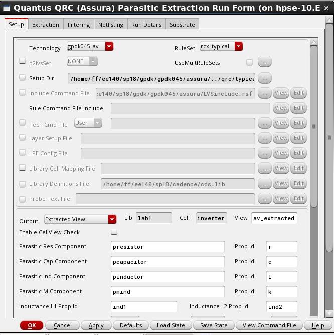
21 If you have any LVS errors, please correct them by making the appropriate adjustments to your layout. Remember to run DRC check again to verify that the update doesn t violate any design rules. At this point, your layout now passes DRC and LVS a huge milestone in the IC design process. Next, we will examine how the physical placement of transistors (layout) impacts circuit performance. 10. Parasitic Extraction with Assura This tool allows us to extract parasitic resistances and capacitances from the layout view. From the menu, click Assura Open Run, and make sure Run Name lists the current cell you are working on ( inverter ). Click OK. Fill-up the form as below and press. Make sure you are pointing to you local gpdk and not to the one in the staff folder. You do not have permission to access it. Now, click Assura Quantus QRC. If you don;t see this tab make sure you cadence_setup described on page-1. Adjust the settings in the setup, extraction, and netlisting tabs to match the screenshots below.
22

23 _ Make sure you have entered gnd! as the REF node. Else the extraction will result in dangling nodes.


24 Click OK to run the parasitic extractor. A successful extraction should give you this message: Return to the library manager, and your inverter cell should have a new view named av_extracted. You can zoom in and see all the little parasitics!


25 The extracted view looks something like below: Once you zoom-in you will find tiny capacitors as below:

26 11. Parasitic Extracted Circuit Simulation We would like to simulate the extracted layout. First, create a new cell view for your inverter_tb cell. This time, select the config tool, making sure the option says Hierarchy Editor. In the New Configuration window, click the Use Template button and select spectre as the template. Change the Top Cell View field from myview to schematic. Now click OK. In the resultant window s menu bar, click View Update. Your windows should look like the screenshots below. Now, right click on the inverter cell and select Set Cell View av_extracted. Update the hierarchy again, then save the configuration.

 _ o x [ile E_dit iew E.lugins t!.elp 1... T_ '-P _C_ _l _lid_l _ '?")

27 I... Virtuoso Hierarchy Editor: New Configuration (Save Needed) Eile E_dit. '{iew lugins lp n 81 I [)..._T_o"'p_C_e1_1?_6_x_.! l Global Bindings _ :J x cadence Libr,.ry: lab1 Libr,.ry List. : yl..ib Cell: invert.er _tb View List.: verilog" "hdl View: schematic St.op List.: spectre Constraint List: Table View C e ll Bindings Tree View "naloglib gpdk045 a:pdk b1 lab1 vpulse n oslv PfflOS1Y inverter inverter _tb spectre spectre spectre schefl'l.!tic scf1ep1atic spectre c110s_ spectre clllos_ spectre c1110s_ spectre c11es_ spectre c..as_. CDBA F ilt.ers: Cf"F II " Virtuoso Hierarchy Editor: (labl inverter_tb config) _ o x [ile E_dit iew E.lugins t!.elp 1... T_ '-P _C_ _l _lid_l _ '? _ _ 1 _ _- _l'i', xl I Global Bindings cadence Library: labl Cell: inverter _tb View: schematic Library List: View List: Stop List: Constraint List: mylib ver iloga ahdl spectre Table View Cell Bindings Tree View analoglib analoglib gpdk045 gpdk045 labl lab1 presistor vdc vpulse nrnoslv prnoslv inverter inverter _tb spectre spectre spectre spectre spectre av_extracted schematic + + av_extracted spectre cmos_ spectre crnos_ spectre crnos_ spectre crnos_ spectre crnos_ spectre crnos_ Narnespace: CDBA Filters: OFF
28 Open up the Library Manager window and double click the inverter_tb config cell view. This prompts you to open the hierarchy configuration (which is what we just edited) and/or the top cell view. If you kept the configuration window open, just open the top cell view. You should now see your inverter_tb schematic. Click on the inverter symbol, then press the x key to descend into the inverter cell. Your regular layout has now been replaced with the extracted one. Press the b key to ascend one level back to the top level schematic. Launch ADE L again. Click Simulation Netlist Create. The netlist should be simulated with all the parasitics included. Look at the parasitics to get a feel for their values. Save a copy of the netlist (either text or screenshot) to include in your lab report. Configure ADE to run the DC sweep and transient simulation again. Find the DC gain and the propagation delays. Are the simulation results different now? 12. Deliverables A. Schematic simulation a. DC Gain b. High-Low Propagation Delay c. Low-High Propagation Delay B. Screenshot of finished inverter layout C. Netlist with extracted parasitics D. Extracted Simulation a. DC Gain b. High-Low Propagation Delay c. Low-High Propagation Delay
Professor Muller Fall 2016 Sameet Ramakrishnan Eric Chang Adapted from prior EE140 and EE141 labs. EE 140/240A Lab 0 Full IC Design Flow
 Professor Muller Fall 2016 Sameet Ramakrishnan Eric Chang Adapted from prior EE140 and EE141 labs EE 140/240A Lab 0 Full IC Design Flow In this lab, you will walk through the full process an analog designer
Cadence IC Design Manual
 Cadence IC Design Manual For EE5518 ZHENG Huan Qun Lin Long Yang Revised on May 2017 Department of Electrical & Computer Engineering National University of Singapore 1 P age Contents 1 INTRODUCTION...
EE 330 Spring 2018 Laboratory 2: Basic Boolean Circuits
 EE 330 Spring 2018 Laboratory 2: Basic Boolean Circuits Contents Objective:... 2 Part 1: Introduction... 2 Part 2 Simulation of a CMOS Inverter... 3 Part 2.1 Attaching technology information... 3 Part
Cadence Virtuoso Schematic Design and Circuit Simulation Tutorial
 Cadence Virtuoso Schematic Design and Circuit Simulation Tutorial Introduction This tutorial is an introduction to schematic capture and circuit simulation for ENGN1600 using Cadence Virtuoso. These courses
CPE/EE 427, CPE 527, VLSI Design I: Tutorial #2, Schematic Capture, DC Analysis, Transient Analysis (Inverter, NAND2)
") CPE/EE 427, CPE 527, VLSI Design I: Tutorial #2, Schematic Capture, DC Analysis, Transient Analysis (Inverter, NAND2) Joel Wilder, Aleksandar Milenkovic, ECE Dept., The University of Alabama in Huntsville
CPE/EE 427, CPE 527, VLSI Design I: Tutorial #2, Schematic Capture, DC Analysis, Transient Analysis (Inverter, NAND2) Joel Wilder, Aleksandar Milenkovic, ECE Dept., The University of Alabama in Huntsville
Amplifier Simulation Tutorial. Design Kit: Cadence 0.18μm CMOS PDK (gpdk180) (Cadence Version 6.1.5)
 (Cadence Version 6.1.5)") Amplifier Simulation Tutorial Design Kit: Cadence 0.18μm CMOS PDK (gpdk180) (Cadence Version 6.1.5) Yongsuk Choi, Marvin Onabajo This tutorial provides a quick introduction to the use of Cadence tools
Amplifier Simulation Tutorial Design Kit: Cadence 0.18μm CMOS PDK (gpdk180) (Cadence Version 6.1.5) Yongsuk Choi, Marvin Onabajo This tutorial provides a quick introduction to the use of Cadence tools
VLSI Lab Tutorial 3. Virtuoso Layout Editing Introduction
 VLSI Lab Tutorial 3 Virtuoso Layout Editing Introduction 1.0 Introduction The purpose of this lab tutorial is to guide you through the design process in creating a custom IC layout for your CMOS inverter
Design rule illustrations for the AMI C5N process can be found at:
 Cadence Tutorial B: Layout, DRC, Extraction, and LVS Created for the MSU VLSI program by Professor A. Mason and the AMSaC lab group. Revised by C Young & Waqar A Qureshi -FS08 Document Contents Introduction
Cadence Tutorial. Introduction to Cadence 0.18um, Implementation and Simulation of an inverter. A. Moradi, A. Miled et M. Sawan
 Cadence Tutorial Introduction to Cadence 0.18um, Implementation and Simulation of an inverter A. Moradi, A. Miled et M. Sawan Section 1: Introduction to Cadence You will see how to create a new library
EE115C Digital Electronic Circuits. Tutorial 4: Schematic-driven Layout (Virtuoso XL)
") EE115C Digital Electronic Circuits Tutorial 4: Schematic-driven Layout (Virtuoso XL) This tutorial will demonstrate schematic-driven layout on the example of a 2-input NAND gate. Simple Layout (that won
EE115C Digital Electronic Circuits Tutorial 4: Schematic-driven Layout (Virtuoso XL) This tutorial will demonstrate schematic-driven layout on the example of a 2-input NAND gate. Simple Layout (that won
Cadence Tutorial: Schematic Entry and Circuit Simulation of a CMOS Inverter
 Cadence Tutorial: Schematic Entry and Circuit Simulation of a CMOS Inverter Introduction This tutorial describes the steps involved in the design and simulation of a CMOS inverter using the Cadence Virtuoso
Virtuoso Layout Editor
 This tutorial will cover the basic steps involved in using the Cadence layout editor called Virtuoso, extracting layout, and running simulation on the layout. The inverter layout is used as an example
Cadence Tutorial A: Schematic Entry and Functional Simulation Created for the MSU VLSI program by Andrew Mason and the AMSaC lab group.
 Cadence Tutorial A: Schematic Entry and Functional Simulation Created for the MSU VLSI program by Andrew Mason and the AMSaC lab group. Revision Notes: Aug. 2003 update and edit A. Mason add intro/revision/contents
EE115C Digital Electronic Circuits. Tutorial 2: Hierarchical Schematic and Simulation
 EE115C Digital Electronic Circuits Tutorial 2: Hierarchical Schematic and Simulation The objectives are to become familiar with Virtuoso schematic editor, learn how to create the symbol view of basic primitives,
EECE 285 VLSI Design. Cadence Tutorial EECE 285 VLSI. By: Kevin Dick Co-author: Jeff Kauppila Co-author: Dr. Arthur Witulski
 Cadence Tutorial EECE 285 VLSI By: Kevin Dick Co-author: Jeff Kauppila Co-author: Dr. Arthur Witulski 1 Table of Contents Purpose of Cadence 1) The Purpose of Cadence pg. 4 Linux 1) The Purpose of Linux
Logging in, starting a shell tool, and starting the Cadence Tool Suite
 EEE 4134 VLSI I Laboratory Lab 0 (Introductory Lab) Logging into Cadence Server, Tool Setup, Cell Library Creation, Introduction to Custom IC Design flow Objectives: To login, start a shell tool and start
Revision Notes: July2004 Generate tutorial for single transistor analysis. Based on existing schematic entry tutorial developed for ECE410
 Cadence Analog Tutorial 1: Schematic Entry and Transistor Characterization Created for the MSU VLSI program by Professor A. Mason and the AMSaC lab group. Revision Notes: July2004 Generate tutorial for
CS755 CAD TOOL TUTORIAL
 CS755 CAD TOOL TUTORIAL CREATING SCHEMATIC IN CADENCE Shi-Ting Zhou shi-ting@cs.wisc.edu After you have figured out what you want to design, and drafted some pictures and diagrams, it s time to input schematics
Microelectronica. Full-Custom Design with Cadence Tutorial
 Área Científica de Electrónica Microelectronica Full-Custom Design with Cadence Tutorial AustriaMicroSystems C35B3 (HIT-Kit 3.70) Marcelino Santos Table of contends 1. Starting Cadence... 3 Starting Cadence
VLSI Lab Tutorial 1. Cadence Virtuoso Schematic Composer Introduction
 VLSI Lab Tutorial 1 Cadence Virtuoso Schematic Composer Introduction 1.0 Introduction The purpose of the first lab tutorial is to help you become familiar with the schematic editor, Virtuoso Schematic
ECE471/571 Energy Efficient VLSI Design Project 2 Cadence Setup and Creation of an Inverter Due Date 11:30 am on Friday, February 2 nd, 2018
 ECE471/571 Energy Efficient VLSI Design Project 2 Cadence Setup and Creation of an Inverter Due Date 11:30 am on Friday, February 2 nd, 2018 Introduction This project will first walk you through the setup
ESE570 Spring University of Pennsylvania Department of Electrical and System Engineering Digital Integrated Cicruits AND VLSI Fundamentals
 University of Pennsylvania Department of Electrical and System Engineering Digital Integrated Cicruits AND VLSI Fundamentals ESE570, Spring 2019 HW5: Delay and Layout Sunday, February 17th Due: Friday,
Experiment 0: Introduction to Cadence
 UNIVERSITY OF CALIFORNIA AT BERKELEY College of Engineering Department of Electrical Engineering and Computer Sciences EE105 Lab Experiments Experiment 0: Introduction to Cadence Contents 1. Introduction...
Lab 1: An Introduction to Cadence
 GIF-4201/GEL-7016 (Micro-électronique) Lab 1: An Introduction to Cadence Schematic, simulation and layout Gabriel Gagnon-Turcotte, Mehdi Noormohammadi Khiarak and Benoit Gosselin Department of Electrical
TUTORIAL II ECE 555 / 755 Updated on September 11 th 2006 CADENCE LAYOUT AND PARASITIC EXTRACTION
 TUTORIAL II ECE 555 / 755 Updated on September 11 th 2006 CADENCE LAYOUT AND PARASITIC EXTRACTION After finishing a schematic of your design (Tutorial-I), the next step is creating masks which are for
Cadence Tutorial 2: Layout, DRC/LVS and Circuit Simulation with Extracted Parasitics
 Cadence Tutorial 2: Layout, DRC/LVS and Circuit Simulation with Extracted Parasitics Introduction This tutorial describes how to generate a mask layout in the Cadence Virtuoso Layout Editor. Use of DIVA
UNIVERSITY OF WATERLOO
 UNIVERSITY OF WATERLOO UW ASIC DESIGN TEAM: Cadence Tutorial Description: Part I: Layout & DRC of a CMOS inverter. Part II: Extraction & LVS of a CMOS inverter. Part III: Post-Layout Simulation. The Cadence
EE 330 Laboratory 3 Layout, DRC, and LVS Fall 2015
 EE 330 Laboratory 3 Layout, DRC, and LVS Fall 2015 Contents Objective:... 2 Part 1 Creating a layout... 2 1.1 Run DRC Early and Often... 2 1.2 Create N active and connect the transistors... 3 1.3 Vias...
ESE 570 Cadence Lab Assignment 2: Introduction to Spectre, Manual Layout Drawing and Post Layout Simulation (PLS)
") ESE 570 Cadence Lab Assignment 2: Introduction to Spectre, Manual Layout Drawing and Post Layout Simulation (PLS) Objective Part A: To become acquainted with Spectre (or HSpice) by simulating an inverter,
ESE 570 Cadence Lab Assignment 2: Introduction to Spectre, Manual Layout Drawing and Post Layout Simulation (PLS) Objective Part A: To become acquainted with Spectre (or HSpice) by simulating an inverter,
EE 330 Spring Laboratory 2: Basic Boolean Circuits
 EE 330 Spring 2013 Laboratory 2: Basic Boolean Circuits Objective: The objective of this experiment is to investigate methods for evaluating the performance of Boolean circuits. Emphasis will be placed
Lab 2. Standard Cell layout.
 Lab 2. Standard Cell layout. The purpose of this lab is to demonstrate CMOS-standard cell design. Use the lab instructions and the cadence manual (http://www.es.lth.se/ugradcourses/cadsys/cadence.html)
EE 330 Laboratory 3 Layout, DRC, and LVS
 EE 330 Laboratory 3 Layout, DRC, and LVS Spring 2018 Contents Objective:... 2 Part 1 creating a layout... 2 1.1 Run DRC... 2 1.2 Stick Diagram to Physical Layer... 3 1.3 Bulk Connections... 3 1.4 Pins...
CS/EE 5720/6720 Analog IC Design Tutorial for Schematic Design and Analysis using Spectre
 CS/EE 5720/6720 Analog IC Design Tutorial for Schematic Design and Analysis using Spectre Introduction to Cadence EDA: The Cadence toolset is a complete microchip EDA (Electronic Design Automation) system,
FACULTY OF ENGINEERING MULTIMEDIA UNIVERSITY LAB SHEET DIGITAL INTEGRATED CIRCUIT
 FACULTY OF ENGINEERING MULTIMEDIA UNIVERSITY LAB SHEET DIGITAL INTEGRATED CIRCUIT DIC1: Schematic Design Entry, Simulation & Verification DIC2: Schematic Driven Layout Drawing (SDL) Design Rule Check (DRC)
ECE 331: Electronics Principles I Fall 2014
 ECE 331: Electronics Principles I Fall 2014 Lab #0: Introduction to Computer Modeling and Laboratory Measurements Report due at your registered lab period on the week of Sept. 8-12 Week 1 Accessing Linux
DOWNLOAD PDF CADENCE WAVEFORM CALCULATOR USER GUIDE
 Chapter 1 : CSE / Cadence Tutorial The Cadence Design Communities support Cadence users and technologists interacting to exchange ideas, news, technical information, and best practices to solve problems
S Exercise 1C Testing the Ring Oscillator
 S-87.3148 Exercise 1C Testing the Ring Oscillator Aalto University School of Electrical Engineering Department of Micro- and Nanosciences (ECDL) 10.9.2014 1 1 Building the test bench In this exercise,
ELEC451 Integrated Circuit Engineering Using Cadence's Virtuoso Layout Editing Tool
 ELEC451 Integrated Circuit Engineering Using Cadence's Virtuoso Layout Editing Tool Contents Contents 1. General 2. Creating and Working On a Layout o 2.1 Undoing/Re-doing an Action o 2.2 Display Options
UNIVERSITY OF CALIFORNIA College of Engineering Department of Electrical Engineering and Computer Sciences Lab #2: Layout and Simulation
 UNIVERSITY OF CALIFORNIA College of Engineering Department of Electrical Engineering and Computer Sciences Lab #2: Layout and Simulation NTU IC541CA 1 Assumed Knowledge This lab assumes use of the Electric
Cadence Tutorial C: Simulating DC and Timing Characteristics 1
 Cadence Tutorial C: Simulating DC and Timing Characteristics Created for the MSU VLSI program by Professor A. Mason and the AMSaC lab group Last updated by Patrick O Hara SS15 Document Contents Introduction
Introduction to laboratory exercises in Digital IC Design.
 Introduction to laboratory exercises in Digital IC Design. A digital ASIC typically consists of four parts: Controller, datapath, memory, and I/O. The digital ASIC below, which is an FFT/IFFT co-processor,
Using Cadence Virtuoso, a UNIX based OrCAD PSpice like program, Remotely on a Windows Machine
 Using Cadence Virtuoso, a UNIX based OrCAD PSpice like program, Remotely on a Windows Machine A. Launch PuTTY. 1. Load the Saved Session that has Enable X11 forwarding and the Host Name is cvl.ece.vt.edu.
Cadence Schematic Tutorial. EEE5320/EEE4306 Fall 2015 University of Florida ECE
 Cadence Schematic Tutorial EEE5320/EEE4306 Fall 2015 University of Florida ECE 1 Remote access You may access the Linux server directly from the NEB Computer Lab using your GatorLink username and password.
Laboratory 3. EE 342 (VLSI Circuit Design) - Using Spectre netlist and Calculator for simulation
 - Using Spectre netlist and Calculator for simulation") EE 342 (VLSI Circuit Design) Laboratory 3 - Using Spectre netlist and Calculator for simulation By Mulong Li, 2013 1 Background knowledge Spectre: is a SPICE-class circuit simulator. It provides the basic
EE 342 (VLSI Circuit Design) Laboratory 3 - Using Spectre netlist and Calculator for simulation By Mulong Li, 2013 1 Background knowledge Spectre: is a SPICE-class circuit simulator. It provides the basic
The original document link is
 Tutorial:Analog Artist with HSPICE The original document link is http://www.eda.ncsu.edu/wiki/tutorial:analog_artist_with_hspice This tutorial will introduce you to the Cadence Environment: specifically
Process technology and introduction to physical
 Neuromorphic Engineering II Lab 3, Spring 2014 1 Lab 3 March 10, 2014 Process technology and introduction to physical layout Today you will start to learn to use the Virtuoso layout editor XL which is
More information can be found in the Cadence manuals Virtuoso Layout Editor User Guide and Cadence Hierarchy Editor User Guide.
 Chapter 6 Building with Layout This chapter consists of two parts. The first describes the generation of layout views and the second deals with the various tools used for verifying the layout, both physical
CMOS Design Lab Manual
 CMOS Design Lab Manual Developed By University Program Team CoreEl Technologies (I) Pvt. Ltd. 1 Objective Objective of this lab is to learn the Mentor Graphics HEP2 tools as well learn the flow of the
Cadence Tutorial A: Schematic Entry and Functional Simulation Created for the MSU VLSI program by Professor A. Mason and the AMSaC lab group.
 Cadence Tutorial A: Schematic Entry and Functional Simulation Created for the MSU VLSI program by Professor A. Mason and the AMSaC lab group. Revision Notes: Jan. 2006 Updated for use with spectre simulator
AMS 0.18 µm PDK Setup and Cadence Tutorial Contributors
 AMS 0.18 µm PDK Setup and Cadence Tutorial Contributors Muhammad Ahmed, Sita Asar, and Ayman Fayed, Power Management Research Lab, https://pmrl.osu.edu, Department of Electrical and Computer Engineering,
CPE/EE 427, CPE 527, VLSI Design I: Tutorial #1, Full Custom VLSI (inverter layout)
") CPE/EE 427, CPE 527, VLSI Design I: Tutorial #1, Full Custom VLSI (inverter layout) Joel Wilder, Aleksandar Milenkovic, ECE Dept., The University of Alabama in Huntsville Adapted from Virginia Tech, Dept.
CPE/EE 427, CPE 527, VLSI Design I: Tutorial #1, Full Custom VLSI (inverter layout) Joel Wilder, Aleksandar Milenkovic, ECE Dept., The University of Alabama in Huntsville Adapted from Virginia Tech, Dept.
EEC 116 Fall 2011 Lab #1 Cadence Schematic Capture and Layout Tutorial
 EEC 116 Fall 2011 Lab #1 Cadence Schematic Capture and Layout Tutorial Dept. of Electrical and Computer Engineering University of California, Davis September 26, 2011 Reading: Rabaey Chapters 1, 2, A,
Creating the inv1 cell WITHOUT power pins
 Simulating with extracted parasitic Let s assume I designed the cell inv1, for which I created the views schematic, symbol and layout. Creating the inv1 cell WITHOUT power pins First, create the inverter
EE434 ASIC & Digital Systems. From Layout to SPICE Simulation (Virtuoso, Calibre, HSpice) Spring 2017 Dae Hyun Kim
 Spring 2017 Dae Hyun Kim") EE434 ASIC & Digital Systems From Layout to SPICE Simulation (Virtuoso, Calibre, HSpice) Spring 2017 Dae Hyun Kim daehyun@eecs.wsu.edu 1 Preparation for Lab2 Download the following file into your working
EE434 ASIC & Digital Systems From Layout to SPICE Simulation (Virtuoso, Calibre, HSpice) Spring 2017 Dae Hyun Kim daehyun@eecs.wsu.edu 1 Preparation for Lab2 Download the following file into your working
Virtuoso Schematic Composer
 is a schematic design tool from Cadence. In this tutorial you will learn how to put electrical components, make wire connections, insert pins and check for connection error. Start Cadence Custom IC Design
Cadence Virtuoso Simulation of a pixel
 MEMS AND MICROSENSORS 2018/2019 Cadence Virtuoso Simulation of a pixel 11/12/2018 Giorgio Mussi giorgio.mussi@polimi.it Introduction In this lab, we will use Cadence Virtuoso to simulate a sub-array of
Select the technology library: NCSU_TechLib_ami06, then press OK.
 ECE 126 Inverter Tutorial: Schematic & Symbol Creation Created for GWU by Anis Nurashikin Nordin & Thomas Farmer Tutorial adapted from: http://www.ee.ttu.edu/ee/cadence/commondirectory/final%20tutorials/digitalcircuitsimulationusingvirtuoso.doc
Fall 2008: EE5323 VLSI Design I using Cadence
 1 of 23 9/17/2008 6:47 PM Fall 2008: EE5323 VLSI Design I using Cadence This tutorial has been adapted from EE5323 offered in Fall 2007. Thanks to Jie Gu, Prof. Chris Kim and Satish Sivaswamy of the University
Tutorial on getting started in Cadence. Advanced Analog Circuits Spring 2015 Instructor: Prof. Harish Krishnaswamy TA: Jahnavi Sharma
 Tutorial on getting started in Cadence Advanced Analog Circuits Spring 2015 Instructor: Prof. Harish Krishnaswamy TA: Jahnavi Sharma Getting Started Start Cadence from the terminal by using the command
Mentor Graphics VLSI CAD Tutorials
 VLSI Design Flow Using Mentor-Graphics Tools Mentor Graphics VLSI CAD Tutorials School of Engineering Santa Clara University Santa Clara, CA 95053 At the Design Center, School of Engineering, of Santa
Lab 1: Cadence Custom IC design tools- Setup, Schematic capture and simulation
 Lab 1: Cadence Custom IC design tools- Setup, Schematic capture and simulation Brittany Duffy EE 330- Integrated Electronics Lab Section B Professor Randy Geiger 1/24/13 Introduction The main goal of this
EE4111 Advanced Analog Electronics Design. Spring 2009 Experiment #4 April 6 ~ April 17
 EE4111 Advanced Analog Electronics Design Spring 2009 Experiment #4 April 6 ~ April 17 Setup Cadence in VLSI Lab 1) Copy files $ cp r /home/grads/ee4111ta ~/ 2) Edit your.cshrc file -- Include the following
PSpice Tutorial. Physics 160 Spring 2006
 PSpice Tutorial This is a tutorial designed to guide you through the simulation assignment included in the first homework set. You may either use the program as installed in the lab, or you may install
ANALOG MICROELECTRONICS ( A)
") ANALOG MICROELECTRONICS (304-534A) IBM 130 nm CMOS Technology An Introduction to Cadence Virtuoso Layout Tool and the Analog Simulation Environment Prepared By - Azhar A. Chowdhury Updated by Ming Yang
ANALOG MICROELECTRONICS (304-534A) IBM 130 nm CMOS Technology An Introduction to Cadence Virtuoso Layout Tool and the Analog Simulation Environment Prepared By - Azhar A. Chowdhury Updated by Ming Yang
Figure 1: ADE Test Editor
 Due to some issues that ADE GXL simulation environment has (probably because of inappropriate setup), we will run simulations in the ADE L design environment, which includes all the necessary tools that
EE 330 Spring 2018 Lab 1: Cadence Custom IC design tools Setup, Schematic capture and simulation
 EE 330 Spring 2018 Lab 1: Cadence Custom IC design tools Setup, Schematic capture and simulation Table of Contents Objective... 2 1. Setup... 2 Set Bash Shell for the account... 2 2. Starting Cadence Custom
EE 330 Laboratory Experiment Number 11
 EE 330 Laboratory Experiment Number 11 Design and Simulation of Digital Circuits using Hardware Description Languages Fall 2017 Contents Purpose:... 3 Background... 3 Part 1: Inverter... 4 1.1 Simulating
Guide to the CSE 577 Lab and Cad tools
 Guide to the CSE 577 Lab and Cad tools 1. Introduction The objective of this tutorial is to give you an overview to (1) setup the Cadence and Synopsys hspice tools for your account in IST 218 Lab, (2)
CMOS VLSI Design Lab 4: Full Chip Assembly
 CMOS VLSI Design Lab 4: Full Chip Assembly In this final lab, you will assemble and simulate your entire MIPS microprocessor! You will build your top level chip cell by connecting the datapath, aludec,
A Tutorial on Using the Cadence Virtuoso Editor to create a CMOS Inverter with CMOSIS5 Technology
 A Tutorial on Using the Cadence Virtuoso Editor to create a CMOS Inverter with CMOSIS Technology Developed by Ted Obuchowicz VLSI/CAD Specialist, Dept. of Electrical and Computer Engineering Concordia
Basic Analog Simulation in Cadence
 York University Department of Electrical Engineering and Computer Science EMIL Tutorial Series Tutorial #1 Basic Analog Simulation in Cadence In this tutorial we step through how to start Cadence (or at
Introduction to CCV and Cadence Virtuoso for Electronic Circuit Simulation
 Introduction to CCV and Cadence Virtuoso for Electronic Circuit Simulation Introduction ENGN1600 will be using the Cadence Virtuoso software suite for its circuit design and SPICE components. Part of the
EE 330 Fall 2017 Lab 1: Cadence Custom IC design tools - Setup, Schematic capture and simulation
 EE 330 Fall 2017 Lab 1: Cadence Custom IC design tools - Setup, Schematic capture and simulation Table of Contents Objective... 2 1. Setup... 2 Set Bash Shell for the account... 2 2. Starting Cadence Custom
ECE471/571 Energy Ecient VLSI Design
 ECE471/571 Energy Ecient VLSI Design Project 2 Cadence Setup and Creation of an Inverter Due Date 11:30pm on Friday, January 30 th 2015 Introduction This project will rst walk you through the setup for
EDA-BASED DESIGN PRACTICAL LABORATORY SESSION No. 3
 LABORATOIRE DE SYSTEMES MICROELECTRONIQUES EPFL STI IMM LSM ELD Station nº 11 CH-1015 Lausanne Téléphone : Fax : E-mail : Site web : +4121 693 6955 +4121 693 6959 lsm@epfl.ch lsm.epfl.ch EDA-BASED DESIGN
ECE425: Introduction to VLSI System Design Machine Problem 3 Due: 11:59pm Friday, Dec. 15 th 2017
 ECE425: Introduction to VLSI System Design Machine Problem 3 Due: 11:59pm Friday, Dec. 15 th 2017 In this MP, you will use automated tools to synthesize the controller module from your MP2 project into
How to Get Started. Figure 3
 Tutorial PSpice How to Get Started To start a simulation, begin by going to the Start button on the Windows toolbar, then select Engineering Tools, then OrCAD Demo. From now on the document menu selection
Composite Layout CS/EE N-type from the top. N-type Transistor. Diffusion Mask. Polysilicon Mask
 Composite Layout CS/EE 6710 Introduction to Layout Inverter Layout Example Layout Design Rules Drawing the mask layers that will be used by the fabrication folks to make the devices Very different from
LTSPICE MANUAL. For Teaching Module EE4415 ZHENG HAUN QUN. December 2016
 LTSPICE MANUAL For Teaching Module EE4415 ZHENG HAUN QUN December 2016 DEPARTMENT OF ELECTRICAL AND COMPUTER ENGINNERING NATIONAL UNIVERSITY OF SINGAPORE Contents 1. Introduction... 2 1.1 Installation...
EE261 Computer Project 1: Using Mentor Graphics for Digital Simulation
 EE261 Computer Project 1: Using Mentor Graphics for Digital Simulation Introduction In this project, you will begin to explore the digital simulation tools of the Mentor Graphics package available on the
Verifying the Multiplexer Layout
 4 This chapter introduces you to interactive verification. You will perform two different tests in the Virtuoso layout editor while using Assura interactive verification products. One test uses the Design
CADENCE SETUP. ECE4430-Analog IC Design
 CADENCE SETUP This short tutorial shows how to configure Cadence to use the NCSU Cadence Design Kit (CDK) with access to the ON Semiconductor C5 0.5-µm and the TSMC 0.35-µm CMOS processes libraries. In
This is a brief tutorial about building a Symbol for a Schematic in Cadence IC design tool environment for hierarchical design of schematics.
 This is a brief tutorial about building a Symbol for a Schematic in Cadence IC design tool environment for hierarchical design of schematics. 1. > cd work035 2. > cadsetup ams035 3. > virtuoso& IMPORTANT:
EE5323/5324 VLSI Design I/II using Cadence
 1 of 18 2009-1-23 23:58 Spring 2009: EE5323/5324 VLSI Design I/II using Cadence This tutorial has been adapted from EE5323 offered in Fall 2007. Thanks to Jie Gu, Prof. Chris Kim and Satish Sivaswamy of
Simulation with Verilog-XL
 Simulation with Verilog-XL Adapted from Princeton Cadence Page (http://www.ee.princeton.edu/~cadence/usr/verilog.html) Until now, we have been using the Analog Environment to do simulations. This simulator
University of California at Berkeley College of Engineering Department of Electrical Engineering and Computer Science. EECS 150 Spring 2000
 University of California at Berkeley College of Engineering Department of Electrical Engineering and Computer Science EECS 150 Spring 2000 Lab 1 Introduction to Xilinx Design Software 1 Objectives In this
Intro to Cadence. Brady Salz. ECE483 Spring 17
 Intro to Cadence Brady Salz ECE483 Spring 17 What We re Doing Learn you a Cadence Learn simulation vocabulary Basic schematic guidelines Simulation results Init Before we begin, open a terminal: $ module
ECE 683 OSU DIGITAL CELL LIBRARY DOCUMENTATION. Matt Silverman 12/5/2005. Timing Characterization Using Cadence
 ECE 683 OSU DIGITAL CELL LIBRARY DOCUMENTATION Matt Silverman 12/5/2005 Timing Characterization Using Cadence TABLE OF CONTENTS INTRODUCTION... 3 TRANSIENT ANALYSIS WITH CADENCE -------------------------------------------------------------------
Cadence Tutorial D: Using Design Variables and Parametric Analysis Document Contents Introduction Using Design Variables Apply Apply
 Cadence Tutorial D: Using Design Variables and Parametric Analysis Created for the MSU VLSI program by Casey Wallace Last Updated by: Patrick O Hara SS15 Document Contents Introduction Using Design Variables
Analog IC Schematic Capture. Mentor Graphics 2006
 Analog IC Schematic Capture Mentor Graphics 2006 Santa Clara University Department of Electrical Engineering Date of Last Revision: February 6, 2007 Table of Contents 1. Objective...3 2. Setup & Preparation...4
Layout and Layout Verification. of an Inverter Circuit
 Layout and Layout Verification of an Inverter Circuit Santa Clara University Department of Electrical Engineering By Piyush Panwar Under Guidance of Dr Samiha Mourad Date of Last Revision: August 7, 2010
EEC 118 Spring 2011 Lab #5 Manchester Carry-Chain Adder
 EEC 118 Spring 2011 Lab #5 Manchester Carry-Chain Adder Rajeevan Amirtharajah Dept. of Electrical and Computer Engineering University of California, Davis Issued: May 9, 2011 Due: May 20, 2011, 5 PM in
University of California at Berkeley College of Engineering Department of Electrical Engineering and Computer Science
 University of California at Berkeley College of Engineering Department of Electrical Engineering and Computer Science EECS 150 Fall 2000 Original Lab By: J.Wawrzynek and N. Weaver Edited by B. Choi, R.
Introduction to PCB Design with EAGLE. Jianan Li
 Introduction to PCB Design with EAGLE Jianan Li Install EAGLE Download EAGLE: http://www.cadsoftusa.com/download-eagle/ Choose Run as Freeware during installation Create a New Project Launch EAGLE and
Introduction to Design Architect
 SANTA CLARA UNIVERSITY Dept. of Electrical Engineering Mentor Graphics Tutorials Introduction to Design Architect Yiching Chen Sangeetha Raman S. Krishnan I. Introduction II. This document contains a step-by-step
TUTORIAL SESSION Technical Group Hoda Najafi & Sunita Bhide
 TUTORIAL SESSION 2014 Technical Group Hoda Najafi & Sunita Bhide SETUP PROCEDURE Start the Altium Designer Software. (Figure 1) Ensure that the Files and Projects tabs are located somewhere on the screen.
EE 471: Transport Phenomena in Solid State Devices
 EE 471: Transport Phenomena in Solid State Devices HW7 Due: 4/17/18 For this homework, you will download a free PC version of the industry standard SPICE circuit simulator called LTspice, provided by Linear
CMOS INVERTER LAYOUT TUTORIAL
 PRINCESS SUMAYA UNIVERSITY FOR TECHNOLOGY CMOS INVERTER LAYOUT TUTORIAL We will start the inverter by drawing a PMOS. The first step is to draw a poly layer. Click on draw a rectangle and choose the poly
Analog IC Simulation. Mentor Graphics 2006
 Analog IC Simulation Mentor Graphics 2006 Santa Clara University Department of Electrical Engineering Date of Last Revision: March 29, 2007 Table of Contents 1. Objective... 3 2. Basic Test Circuit Creation...
Setting up an initial ".tcshrc" file
 ECE445 Fall 2005 Introduction to SaberSketch The SABER simulator is a tool for computer simulation of analog systems, digital systems and mixed signal systems. SaberDesigner consists of the three tools,