This is a brief tutorial about building a Symbol for a Schematic in Cadence IC design tool environment for hierarchical design of schematics.
|
|
|
- Shauna Curtis
- 5 years ago
- Views:
Transcription


 Build it in {work035} directory.")
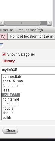
1 This is a brief tutorial about building a Symbol for a Schematic in Cadence IC design tool environment for hierarchical design of schematics. 1. > cd work > cadsetup ams > virtuoso& IMPORTANT: You should be seeing following splash windows. If you have not, that means you did not setup the class technology on the directory that you invoked/run Cadence. Splash screens This is Cadence CIW window 4. Run library manager. (CIW: Tools ->Library Manager ) SKIP IF: If you already build a library before using class technology library, skip steps 5-8, and go to step Build a new library. (Library Manager: File->New->Library ) Build it in {work035} directory. Name it something you will use throughout the semester (i.e. mylib035). <OK> Cadence Tutorials Page 1 of 8 T1.Rev.1.0


2 6. Attach and exiting library. <OK> 7. Choose class technology file TECH_C35B4. <OK> 8. Your new library will be listed on the Library list. Cadence Tutorials Page 2 of 8 T1.Rev.1.0


 Give the cell")
3 9. Make sure that your library has correct technology attached. (LIBRARY MANAGER: { Right Click} on library name -> Properties ) techlibname = TECH_C35B4 10. Build a new schematic cell view in your library. (LIBRARY MANAGER: File-> >New->Cell View ) Give the cell a name such as inv_x1. <OK> Cadence Tutorials Page 3 of 8 T1.Rev.1..0
 or")

4 11. Bring primitives from PRIMLIB and a. Click on Create Instance button on Schematic Editor window (SEW) or (SEW:Create->Instance ) or hit i b. Click on Browse on Add Instance window c. Select nmos4 symbol from PRIMLIB, and place it on SEW d. Follow 11.a-c and place a pmos4 symbol on SEW Cadence Tutorials Page 4 of 8 T1.Rev.1.0

 or hit p Cadence")
5 12. Add input, output, supply and ground pins to the schematic as shown below. Click on Create Pin on SEW or (SEW:Create->Pin ) or hit p Cadence Tutorials Page 5 of 8 T1.Rev.1.0


6 13. Wire connect the transistors and pins to form digital inverter circuit, as shown and Check and Save your schematic. Check CIW and make sure that no error exists on the schematic that you just completed. If warnings and/or errors exist, fix them before moving forward ( i.e. following) Cadence Tutorials Page 6 of 8 T1.Rev.1..0


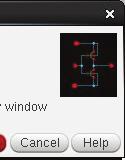
7 14. Build a Symbol for your inverter schematic. (SEW: Creat->Cellview->From Cellview ). a. <OK> for next window. b. Select location where the pins located on the new symbol, <OK> c. Reshape the symbol ay you like. For example, change the symbol using standard digital representation of the inverter using shapes on the symbol window. d. Check and Save and make sure that no error or warning on the symbol. Cadence Tutorials Page 7 of 8 T1.Rev.1.0


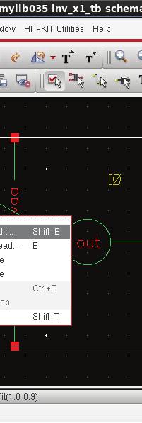


8 Now you can instantiate you inverter cell symbol on any other schematic (i.e. in a new schematic cell, inv_x1_tb). You can go into your schematic by goingg down in the hierarchy. Select the symbol, and (SEW:Edit->Hierarchy- >Descent Edit ) or hit {Shift+E}. Go back up in the hierarchy (SEW: Edit->Hierarcy->Return) or hit {Ctrl+ E} You can edit or read the cell that is descended. Also you can open on same window tab, or a new tab, or Cadence Tutorials Page 8 of 8 T1.Rev.1..0
Select the technology library: NCSU_TechLib_ami06, then press OK.
 ECE 126 Inverter Tutorial: Schematic & Symbol Creation Created for GWU by Anis Nurashikin Nordin & Thomas Farmer Tutorial adapted from: http://www.ee.ttu.edu/ee/cadence/commondirectory/final%20tutorials/digitalcircuitsimulationusingvirtuoso.doc
Virtuoso Schematic Composer
 is a schematic design tool from Cadence. In this tutorial you will learn how to put electrical components, make wire connections, insert pins and check for connection error. Start Cadence Custom IC Design
CS755 CAD TOOL TUTORIAL
 CS755 CAD TOOL TUTORIAL CREATING SCHEMATIC IN CADENCE Shi-Ting Zhou shi-ting@cs.wisc.edu After you have figured out what you want to design, and drafted some pictures and diagrams, it s time to input schematics
ELEC 301 Lab 2: Cadence Basic
 ELEC 301 Lab 2: Cadence Basic Revision: 2.1 Last modified: Aug. 98 Introduction In this class, you will be introduced to the Cadence suit of IC design tools. These tools are a very powerful set of tools.
VLSI Lab Tutorial 1. Cadence Virtuoso Schematic Composer Introduction
 VLSI Lab Tutorial 1 Cadence Virtuoso Schematic Composer Introduction 1.0 Introduction The purpose of the first lab tutorial is to help you become familiar with the schematic editor, Virtuoso Schematic
Cadence Tutorial: Schematic Entry and Circuit Simulation of a CMOS Inverter
 Cadence Tutorial: Schematic Entry and Circuit Simulation of a CMOS Inverter Introduction This tutorial describes the steps involved in the design and simulation of a CMOS inverter using the Cadence Virtuoso
ECE471/571 Energy Efficient VLSI Design Project 2 Cadence Setup and Creation of an Inverter Due Date 11:30 am on Friday, February 2 nd, 2018
 ECE471/571 Energy Efficient VLSI Design Project 2 Cadence Setup and Creation of an Inverter Due Date 11:30 am on Friday, February 2 nd, 2018 Introduction This project will first walk you through the setup
CPE/EE 427, CPE 527, VLSI Design I: Tutorial #2, Schematic Capture, DC Analysis, Transient Analysis (Inverter, NAND2)
") CPE/EE 427, CPE 527, VLSI Design I: Tutorial #2, Schematic Capture, DC Analysis, Transient Analysis (Inverter, NAND2) Joel Wilder, Aleksandar Milenkovic, ECE Dept., The University of Alabama in Huntsville
CPE/EE 427, CPE 527, VLSI Design I: Tutorial #2, Schematic Capture, DC Analysis, Transient Analysis (Inverter, NAND2) Joel Wilder, Aleksandar Milenkovic, ECE Dept., The University of Alabama in Huntsville
AMS 0.18 µm PDK Setup and Cadence Tutorial Contributors
 AMS 0.18 µm PDK Setup and Cadence Tutorial Contributors Muhammad Ahmed, Sita Asar, and Ayman Fayed, Power Management Research Lab, https://pmrl.osu.edu, Department of Electrical and Computer Engineering,
VLSI Lab Tutorial 3. Virtuoso Layout Editing Introduction
 VLSI Lab Tutorial 3 Virtuoso Layout Editing Introduction 1.0 Introduction The purpose of this lab tutorial is to guide you through the design process in creating a custom IC layout for your CMOS inverter
EE115C Digital Electronic Circuits. Tutorial 2: Hierarchical Schematic and Simulation
 EE115C Digital Electronic Circuits Tutorial 2: Hierarchical Schematic and Simulation The objectives are to become familiar with Virtuoso schematic editor, learn how to create the symbol view of basic primitives,
TUTORIAL II ECE 555 / 755 Updated on September 11 th 2006 CADENCE LAYOUT AND PARASITIC EXTRACTION
 TUTORIAL II ECE 555 / 755 Updated on September 11 th 2006 CADENCE LAYOUT AND PARASITIC EXTRACTION After finishing a schematic of your design (Tutorial-I), the next step is creating masks which are for
Schematics. Prof. Dr. P. Fischer. Lehrstuhl für Schaltungstechnik und Simulation Uni Heidelberg
 Schematics Prof. Dr. P. Fischer Lehrstuhl für Schaltungstechnik und Simulation Uni Heidelberg VLSI Design: Schematics P. Fischer, ZITI, Uni Heidelberg Page1 What are Symbols? Very often, a circuit (schematic)
EE115C Digital Electronic Circuits. Tutorial 4: Schematic-driven Layout (Virtuoso XL)
") EE115C Digital Electronic Circuits Tutorial 4: Schematic-driven Layout (Virtuoso XL) This tutorial will demonstrate schematic-driven layout on the example of a 2-input NAND gate. Simple Layout (that won
EE115C Digital Electronic Circuits Tutorial 4: Schematic-driven Layout (Virtuoso XL) This tutorial will demonstrate schematic-driven layout on the example of a 2-input NAND gate. Simple Layout (that won
Introduction to Design Architect
 SANTA CLARA UNIVERSITY Dept. of Electrical Engineering Mentor Graphics Tutorials Introduction to Design Architect Yiching Chen Sangeetha Raman S. Krishnan I. Introduction II. This document contains a step-by-step
Virtuoso Layout Editor
 This tutorial will cover the basic steps involved in using the Cadence layout editor called Virtuoso, extracting layout, and running simulation on the layout. The inverter layout is used as an example
EE 330 Spring 2018 Laboratory 2: Basic Boolean Circuits
 EE 330 Spring 2018 Laboratory 2: Basic Boolean Circuits Contents Objective:... 2 Part 1: Introduction... 2 Part 2 Simulation of a CMOS Inverter... 3 Part 2.1 Attaching technology information... 3 Part
Lab 2. Standard Cell layout.
 Lab 2. Standard Cell layout. The purpose of this lab is to demonstrate CMOS-standard cell design. Use the lab instructions and the cadence manual (http://www.es.lth.se/ugradcourses/cadsys/cadence.html)
CADENCE SETUP. ECE4430-Analog IC Design
 CADENCE SETUP This short tutorial shows how to configure Cadence to use the NCSU Cadence Design Kit (CDK) with access to the ON Semiconductor C5 0.5-µm and the TSMC 0.35-µm CMOS processes libraries. In
Another view of the standard cells called the abstract view needs to generated
 Abstract Generation Place and route tools do not require the full cell layout Another view of the standard cells called the abstract view needs to generated The abstract view provides information like:
EECE 285 VLSI Design. Cadence Tutorial EECE 285 VLSI. By: Kevin Dick Co-author: Jeff Kauppila Co-author: Dr. Arthur Witulski
 Cadence Tutorial EECE 285 VLSI By: Kevin Dick Co-author: Jeff Kauppila Co-author: Dr. Arthur Witulski 1 Table of Contents Purpose of Cadence 1) The Purpose of Cadence pg. 4 Linux 1) The Purpose of Linux
Revision Notes: July2004 Generate tutorial for single transistor analysis. Based on existing schematic entry tutorial developed for ECE410
 Cadence Analog Tutorial 1: Schematic Entry and Transistor Characterization Created for the MSU VLSI program by Professor A. Mason and the AMSaC lab group. Revision Notes: July2004 Generate tutorial for
Cadence Tutorial A: Schematic Entry and Functional Simulation Created for the MSU VLSI program by Andrew Mason and the AMSaC lab group.
 Cadence Tutorial A: Schematic Entry and Functional Simulation Created for the MSU VLSI program by Andrew Mason and the AMSaC lab group. Revision Notes: Aug. 2003 update and edit A. Mason add intro/revision/contents
DOWNLOAD PDF CADENCE WAVEFORM CALCULATOR USER GUIDE
 Chapter 1 : CSE / Cadence Tutorial The Cadence Design Communities support Cadence users and technologists interacting to exchange ideas, news, technical information, and best practices to solve problems
ECE 331: Electronics Principles I Fall 2014
 ECE 331: Electronics Principles I Fall 2014 Lab #0: Introduction to Computer Modeling and Laboratory Measurements Report due at your registered lab period on the week of Sept. 8-12 Week 1 Accessing Linux
Design rule illustrations for the AMI C5N process can be found at:
 Cadence Tutorial B: Layout, DRC, Extraction, and LVS Created for the MSU VLSI program by Professor A. Mason and the AMSaC lab group. Revised by C Young & Waqar A Qureshi -FS08 Document Contents Introduction
Virtuoso Schematic Composer VHDL Interface. VHDL In for Design Framework II:
 Virtuoso Schematic Composer VHDL Interface. VHDL In for Design Framework II: VHDL In for Design Framework II can convert a VHDL structural or behavioral description into one of three forms in Cadence database
Cadence Tutorial. Introduction to Cadence 0.18um, Implementation and Simulation of an inverter. A. Moradi, A. Miled et M. Sawan
 Cadence Tutorial Introduction to Cadence 0.18um, Implementation and Simulation of an inverter A. Moradi, A. Miled et M. Sawan Section 1: Introduction to Cadence You will see how to create a new library
EE4111 Advanced Analog Electronics Design. Spring 2009 Experiment #4 April 6 ~ April 17
 EE4111 Advanced Analog Electronics Design Spring 2009 Experiment #4 April 6 ~ April 17 Setup Cadence in VLSI Lab 1) Copy files $ cp r /home/grads/ee4111ta ~/ 2) Edit your.cshrc file -- Include the following
CPE/EE 427, CPE 527, VLSI Design I: Tutorial #1, Full Custom VLSI (inverter layout)
") CPE/EE 427, CPE 527, VLSI Design I: Tutorial #1, Full Custom VLSI (inverter layout) Joel Wilder, Aleksandar Milenkovic, ECE Dept., The University of Alabama in Huntsville Adapted from Virginia Tech, Dept.
CPE/EE 427, CPE 527, VLSI Design I: Tutorial #1, Full Custom VLSI (inverter layout) Joel Wilder, Aleksandar Milenkovic, ECE Dept., The University of Alabama in Huntsville Adapted from Virginia Tech, Dept.
ANALOG MICROELECTRONICS ( A)
") ANALOG MICROELECTRONICS (304-534A) IBM 130 nm CMOS Technology An Introduction to Cadence Virtuoso Layout Tool and the Analog Simulation Environment Prepared By - Azhar A. Chowdhury Updated by Ming Yang
ANALOG MICROELECTRONICS (304-534A) IBM 130 nm CMOS Technology An Introduction to Cadence Virtuoso Layout Tool and the Analog Simulation Environment Prepared By - Azhar A. Chowdhury Updated by Ming Yang
Cadence Tutorial A: Schematic Entry and Functional Simulation Created for the MSU VLSI program by Professor A. Mason and the AMSaC lab group.
 Cadence Tutorial A: Schematic Entry and Functional Simulation Created for the MSU VLSI program by Professor A. Mason and the AMSaC lab group. Revision Notes: Jan. 2006 Updated for use with spectre simulator
The original document link is
 Tutorial:Analog Artist with HSPICE The original document link is http://www.eda.ncsu.edu/wiki/tutorial:analog_artist_with_hspice This tutorial will introduce you to the Cadence Environment: specifically
EE 330 Laboratory 3 Layout, DRC, and LVS Fall 2015
 EE 330 Laboratory 3 Layout, DRC, and LVS Fall 2015 Contents Objective:... 2 Part 1 Creating a layout... 2 1.1 Run DRC Early and Often... 2 1.2 Create N active and connect the transistors... 3 1.3 Vias...
ECE471/571 Energy Ecient VLSI Design
 ECE471/571 Energy Ecient VLSI Design Project 2 Cadence Setup and Creation of an Inverter Due Date 11:30pm on Friday, January 30 th 2015 Introduction This project will rst walk you through the setup for
UNIVERSITY OF WATERLOO
 UNIVERSITY OF WATERLOO UW ASIC DESIGN TEAM: Cadence Tutorial Description: Part I: Layout & DRC of a CMOS inverter. Part II: Extraction & LVS of a CMOS inverter. Part III: Post-Layout Simulation. The Cadence
Cadence Schematic Tutorial. EEE5320/EEE4306 Fall 2015 University of Florida ECE
 Cadence Schematic Tutorial EEE5320/EEE4306 Fall 2015 University of Florida ECE 1 Remote access You may access the Linux server directly from the NEB Computer Lab using your GatorLink username and password.
Cadence IC Design Manual
 Cadence IC Design Manual For EE5518 ZHENG Huan Qun Lin Long Yang Revised on May 2017 Department of Electrical & Computer Engineering National University of Singapore 1 P age Contents 1 INTRODUCTION...
EE 330 Spring Laboratory 2: Basic Boolean Circuits
 EE 330 Spring 2013 Laboratory 2: Basic Boolean Circuits Objective: The objective of this experiment is to investigate methods for evaluating the performance of Boolean circuits. Emphasis will be placed
Microelectronica. Full-Custom Design with Cadence Tutorial
 Área Científica de Electrónica Microelectronica Full-Custom Design with Cadence Tutorial AustriaMicroSystems C35B3 (HIT-Kit 3.70) Marcelino Santos Table of contends 1. Starting Cadence... 3 Starting Cadence
Amplifier Simulation Tutorial. Design Kit: Cadence 0.18μm CMOS PDK (gpdk180) (Cadence Version 6.1.5)
 (Cadence Version 6.1.5)") Amplifier Simulation Tutorial Design Kit: Cadence 0.18μm CMOS PDK (gpdk180) (Cadence Version 6.1.5) Yongsuk Choi, Marvin Onabajo This tutorial provides a quick introduction to the use of Cadence tools
Amplifier Simulation Tutorial Design Kit: Cadence 0.18μm CMOS PDK (gpdk180) (Cadence Version 6.1.5) Yongsuk Choi, Marvin Onabajo This tutorial provides a quick introduction to the use of Cadence tools
Cadence Tutorial D: Using Design Variables and Parametric Analysis Document Contents Introduction Using Design Variables Apply Apply
 Cadence Tutorial D: Using Design Variables and Parametric Analysis Created for the MSU VLSI program by Casey Wallace Last Updated by: Patrick O Hara SS15 Document Contents Introduction Using Design Variables
EE434 ASIC & Digital Systems. From Layout to SPICE Simulation (Virtuoso, Calibre, HSpice) Spring 2017 Dae Hyun Kim
 Spring 2017 Dae Hyun Kim") EE434 ASIC & Digital Systems From Layout to SPICE Simulation (Virtuoso, Calibre, HSpice) Spring 2017 Dae Hyun Kim daehyun@eecs.wsu.edu 1 Preparation for Lab2 Download the following file into your working
EE434 ASIC & Digital Systems From Layout to SPICE Simulation (Virtuoso, Calibre, HSpice) Spring 2017 Dae Hyun Kim daehyun@eecs.wsu.edu 1 Preparation for Lab2 Download the following file into your working
Tutorial on getting started in Cadence. Advanced Analog Circuits Spring 2015 Instructor: Prof. Harish Krishnaswamy TA: Jahnavi Sharma
 Tutorial on getting started in Cadence Advanced Analog Circuits Spring 2015 Instructor: Prof. Harish Krishnaswamy TA: Jahnavi Sharma Getting Started Start Cadence from the terminal by using the command
Guide to the CSE 577 Lab and Cad tools
 Guide to the CSE 577 Lab and Cad tools 1. Introduction The objective of this tutorial is to give you an overview to (1) setup the Cadence and Synopsys hspice tools for your account in IST 218 Lab, (2)
EEC 116 Fall 2011 Lab #3: Digital Simulation Tutorial
 EEC 116 Fall 2011 Lab #3: Digital Simulation Tutorial Dept. of Electrical and Computer Engineering University of California, Davis Issued: October 10, 2011 Due: October 19, 2011, 4PM Reading: Rabaey Insert
Creating the inv1 cell WITHOUT power pins
 Simulating with extracted parasitic Let s assume I designed the cell inv1, for which I created the views schematic, symbol and layout. Creating the inv1 cell WITHOUT power pins First, create the inverter
Creating LEF File. Abstract Generation: Creating LEF Tutorial File Release Date: 01/13/2004. Export GDS:
 Creating LEF Tutorial 1-1 - Creating LEF File Abstract Generation: Export GDS: Abstract generator comes as a part of the Silicon Ensemble package. As such, it cannot directly read ICFB library databases.
EE 330 Laboratory 3 Layout, DRC, and LVS
 EE 330 Laboratory 3 Layout, DRC, and LVS Spring 2018 Contents Objective:... 2 Part 1 creating a layout... 2 1.1 Run DRC... 2 1.2 Stick Diagram to Physical Layer... 3 1.3 Bulk Connections... 3 1.4 Pins...
Prepared by Dr. Ulkuhan Guler GT-Bionics Lab Georgia Institute of Technology
 Prepared by Dr. Ulkuhan Guler GT-Bionics Lab Georgia Institute of Technology OUTLINE Introduction Mapping for Schematic and Layout Connectivity Generate Layout from Schematic Connectivity Some Useful Features
Analog IC Schematic Capture. Mentor Graphics 2006
 Analog IC Schematic Capture Mentor Graphics 2006 Santa Clara University Department of Electrical Engineering Date of Last Revision: February 6, 2007 Table of Contents 1. Objective...3 2. Setup & Preparation...4
Abstract Editor (Last updated: Oct. 23, 2008)
") Abstract Editor (Last updated: Oct. 23, 2008) Abstract Editor Tutorial This tutorial has been created to discuss all of the steps needed to create an abstract Library Exchange Format (LEF) file for custom
Abstract Editor (Last updated: Oct. 23, 2008) Abstract Editor Tutorial This tutorial has been created to discuss all of the steps needed to create an abstract Library Exchange Format (LEF) file for custom
Cadence Analog Circuit Tutorial
 Cadence Analog Circuit Tutorial Schematic Entry for Analog Designs- Passive Circuits (RLC Circuit) In this tutorial, we will build the circuit shown in figure 1 below, using the Cadence Composer tool.
Using Cadence Virtuoso, a UNIX based OrCAD PSpice like program, Remotely on a Windows Machine
 Using Cadence Virtuoso, a UNIX based OrCAD PSpice like program, Remotely on a Windows Machine A. Launch PuTTY. 1. Load the Saved Session that has Enable X11 forwarding and the Host Name is cvl.ece.vt.edu.
CMOS Design Lab Manual
 CMOS Design Lab Manual Developed By University Program Team CoreEl Technologies (I) Pvt. Ltd. 1 Objective Objective of this lab is to learn the Mentor Graphics HEP2 tools as well learn the flow of the
DRC and LVS checks using Cadence Virtuoso Version 2.0
 DRC and LVS checks using Cadence Virtuoso Version 2.0 Start virtuoso l l Open a virtuoso session in the directory which contains the required cds.lib and lib.def files. Command : virtuoso & Open the layout
Cadence Tutorial 2: Layout, DRC/LVS and Circuit Simulation with Extracted Parasitics
 Cadence Tutorial 2: Layout, DRC/LVS and Circuit Simulation with Extracted Parasitics Introduction This tutorial describes how to generate a mask layout in the Cadence Virtuoso Layout Editor. Use of DIVA
EEC 116 Fall 2011 Lab #1 Cadence Schematic Capture and Layout Tutorial
 EEC 116 Fall 2011 Lab #1 Cadence Schematic Capture and Layout Tutorial Dept. of Electrical and Computer Engineering University of California, Davis September 26, 2011 Reading: Rabaey Chapters 1, 2, A,
Introduction to laboratory exercises in Digital IC Design.
 Introduction to laboratory exercises in Digital IC Design. A digital ASIC typically consists of four parts: Controller, datapath, memory, and I/O. The digital ASIC below, which is an FFT/IFFT co-processor,
UNIVERSITY OF CALIFORNIA College of Engineering Department of Electrical Engineering and Computer Sciences Lab #2: Layout and Simulation
 UNIVERSITY OF CALIFORNIA College of Engineering Department of Electrical Engineering and Computer Sciences Lab #2: Layout and Simulation NTU IC541CA 1 Assumed Knowledge This lab assumes use of the Electric
Experiment 0: Introduction to Cadence
 UNIVERSITY OF CALIFORNIA AT BERKELEY College of Engineering Department of Electrical Engineering and Computer Sciences EE105 Lab Experiments Experiment 0: Introduction to Cadence Contents 1. Introduction...
Fall 2008: EE5323 VLSI Design I using Cadence
 1 of 23 9/17/2008 6:47 PM Fall 2008: EE5323 VLSI Design I using Cadence This tutorial has been adapted from EE5323 offered in Fall 2007. Thanks to Jie Gu, Prof. Chris Kim and Satish Sivaswamy of the University
EE 330 Laboratory Experiment Number 11
 EE 330 Laboratory Experiment Number 11 Design and Simulation of Digital Circuits using Hardware Description Languages Fall 2017 Contents Purpose:... 3 Background... 3 Part 1: Inverter... 4 1.1 Simulating
Cadence Virtuoso Schematic Design and Circuit Simulation Tutorial
 Cadence Virtuoso Schematic Design and Circuit Simulation Tutorial Introduction This tutorial is an introduction to schematic capture and circuit simulation for ENGN1600 using Cadence Virtuoso. These courses
Basic Analog Simulation in Cadence
 York University Department of Electrical Engineering and Computer Science EMIL Tutorial Series Tutorial #1 Basic Analog Simulation in Cadence In this tutorial we step through how to start Cadence (or at
Introduction to CCV and Cadence Virtuoso for Electronic Circuit Simulation
 Introduction to CCV and Cadence Virtuoso for Electronic Circuit Simulation Introduction ENGN1600 will be using the Cadence Virtuoso software suite for its circuit design and SPICE components. Part of the
HOMEWORK 9 CMPEN 411 Due: 4/12/ :30pm
 HOMEWORK 9 CMPEN 411 Due: 4/12/2016 11:30pm Learning Objective Complete the full 8 bit RISC microprocessor chip design by placing the processor core design into the 40 pin 'tiny' chip pad frame. Do verify
RFIC Dynamic Link September 2004
 RFIC Dynamic Link September 2004 Notice The information contained in this document is subject to change without notice. Agilent Technologies makes no warranty of any kind with regard to this material,
Creating Verilog Tutorial Netlist Release Date: 01/13/2005(Version 2)
") Creating Verilog Tutorial 2-1 - Creating a verilog netlist for a schematic: The verilog netlist is necessary for automatic layout (placement and routing) tools. It contains information about the I/O pins
Creating Verilog Tutorial 2-1 - Creating a verilog netlist for a schematic: The verilog netlist is necessary for automatic layout (placement and routing) tools. It contains information about the I/O pins
University of California, Berkeley College of Engineering Department of Electrical Engineering and Computer Science
 University of California, Berkeley College of Engineering Department of Electrical Engineering and Computer Science EE240B Spring 2018 Eric Chang, Prof. Elad Alon Virtuoso/ADEXL/BAG tutorial This tutorial
Verifying the Multiplexer Layout
 4 This chapter introduces you to interactive verification. You will perform two different tests in the Virtuoso layout editor while using Assura interactive verification products. One test uses the Design
A Tutorial on Using the Cadence Virtuoso Editor to create a CMOS Inverter with CMOSIS5 Technology
 A Tutorial on Using the Cadence Virtuoso Editor to create a CMOS Inverter with CMOSIS Technology Developed by Ted Obuchowicz VLSI/CAD Specialist, Dept. of Electrical and Computer Engineering Concordia
CS/EE 5720/6720 Analog IC Design Tutorial for Schematic Design and Analysis using Spectre
 CS/EE 5720/6720 Analog IC Design Tutorial for Schematic Design and Analysis using Spectre Introduction to Cadence EDA: The Cadence toolset is a complete microchip EDA (Electronic Design Automation) system,
More information can be found in the Cadence manuals Virtuoso Layout Editor User Guide and Cadence Hierarchy Editor User Guide.
 Chapter 6 Building with Layout This chapter consists of two parts. The first describes the generation of layout views and the second deals with the various tools used for verifying the layout, both physical
HOMEWORK 10 CMPEN 411 Due: 4/28/ :30pm
 HOMEWORK 10 CMPEN 411 Due: 4/28/2016 11:30pm Instruction First, fabrication ready the full 8 bit RISC microprocessor chip: redesign the chip (its components) to fit the entire chip fitted into the 40 pin
Mixed Signal Design Simulation Manual
 CADENCE Mixed Signal Design Simulation Manual Version 1.0 By Zheng Huan Qun February 2005 Department of Electrical and Computer Engineering National University of Singapore ACKNOWLEDGMENTS The author would
DRC and LVS checks using Cadence Virtuoso Version 3.0
 DRC and LVS checks using Cadence Virtuoso Version 3.0 Start virtuoso l l Open a virtuoso session in the directory which contains the required cds.lib and lib.def files. Command : virtuoso & Open the layout
S Exercise 1C Testing the Ring Oscillator
 S-87.3148 Exercise 1C Testing the Ring Oscillator Aalto University School of Electrical Engineering Department of Micro- and Nanosciences (ECDL) 10.9.2014 1 1 Building the test bench In this exercise,
EE 330 Laboratory Experiment Number 11 Design and Simulation of Digital Circuits using Hardware Description Languages
 EE 330 Laboratory Experiment Number 11 Design and Simulation of Digital Circuits using Hardware Description Languages Fall 2015 Purpose: The purpose of this experiment is to develop methods for using Hardware
Cadence Tutorial C: Simulating DC and Timing Characteristics 1
 Cadence Tutorial C: Simulating DC and Timing Characteristics Created for the MSU VLSI program by Professor A. Mason and the AMSaC lab group Last updated by Patrick O Hara SS15 Document Contents Introduction
EECS 627, Lab Assignment 3
 EECS 627, Lab Assignment 3 1 Introduction In this lab assignment, we will use Cadence ICFB and Calibre to become familiar with the process of DRC/LVS checks on a design. So far, we have placed and routed
DC Circuit Simulation
 Chapter 2 DC Circuit Simulation 2.1 Starting the Project Manager 1. Select Project Manager from the Start All Program Cadence Release 16.5 Project Manager. 2. Select Allegro PCB Designer (Schematic) from
Professor Muller Fall 2016 Sameet Ramakrishnan Eric Chang Adapted from prior EE140 and EE141 labs. EE 140/240A Lab 0 Full IC Design Flow
 Professor Muller Fall 2016 Sameet Ramakrishnan Eric Chang Adapted from prior EE140 and EE141 labs EE 140/240A Lab 0 Full IC Design Flow In this lab, you will walk through the full process an analog designer
Altera Quartus II Tutorial ECE 552
 Altera Quartus II Tutorial ECE 552 Quartus II by Altera is a PLD Design Software which is suitable for high-density Field-Programmable Gate Array (FPGA) designs, low-cost FPGA designs, and Complex Programmable
FACULTY OF ENGINEERING MULTIMEDIA UNIVERSITY LAB SHEET DIGITAL INTEGRATED CIRCUIT
 FACULTY OF ENGINEERING MULTIMEDIA UNIVERSITY LAB SHEET DIGITAL INTEGRATED CIRCUIT DIC1: Schematic Design Entry, Simulation & Verification DIC2: Schematic Driven Layout Drawing (SDL) Design Rule Check (DRC)
Lab 1: Cadence Custom IC design tools- Setup, Schematic capture and simulation
 Lab 1: Cadence Custom IC design tools- Setup, Schematic capture and simulation Brittany Duffy EE 330- Integrated Electronics Lab Section B Professor Randy Geiger 1/24/13 Introduction The main goal of this
Beginners manual for Cadence
 Starting the Cadence for the first time. Beginners manual for Cadence Drawing 1: Cadence initialization (terminal window) Follow these steps [Drawing 1]: create new subdirectory ( use 'mkdir' command for
EE5323/5324 VLSI Design I/II using Cadence
 1 of 18 2009-1-23 23:58 Spring 2009: EE5323/5324 VLSI Design I/II using Cadence This tutorial has been adapted from EE5323 offered in Fall 2007. Thanks to Jie Gu, Prof. Chris Kim and Satish Sivaswamy of
Mentor Graphics VLSI CAD Tutorials
 VLSI Design Flow Using Mentor-Graphics Tools Mentor Graphics VLSI CAD Tutorials School of Engineering Santa Clara University Santa Clara, CA 95053 At the Design Center, School of Engineering, of Santa
ESE570 Spring University of Pennsylvania Department of Electrical and System Engineering Digital Integrated Cicruits AND VLSI Fundamentals
 University of Pennsylvania Department of Electrical and System Engineering Digital Integrated Cicruits AND VLSI Fundamentals ESE570, Spring 2019 HW5: Delay and Layout Sunday, February 17th Due: Friday,
TUTORIAL 1. V1.1 Update on Sept 17, 2003 ECE 755. Part 1: Design Architect IC
 TUTORIAL 1 V1.1 Update on Sept 17, 2003 ECE 755 Part 1: Design Architect IC DA-IC provides a design environment comprising tools to create schematics, symbols and run simulations. The schematic editor
Intro to Cadence. Brady Salz. ECE483 Spring 17
 Intro to Cadence Brady Salz ECE483 Spring 17 What We re Doing Learn you a Cadence Learn simulation vocabulary Basic schematic guidelines Simulation results Init Before we begin, open a terminal: $ module
How to Get Started. Figure 3
 Tutorial PSpice How to Get Started To start a simulation, begin by going to the Start button on the Windows toolbar, then select Engineering Tools, then OrCAD Demo. From now on the document menu selection
Figure 1: ADE Test Editor
 Due to some issues that ADE GXL simulation environment has (probably because of inappropriate setup), we will run simulations in the ADE L design environment, which includes all the necessary tools that
ECEN 474 Homework #2 Notes
 ECEN 474 Homework #2 Notes February 22, 2018 Due: 3-6-2018, 5:00PM Homeworks will not be received after due. Instructor: Sam Palermo 1. (50 points) Technology Characterization for Design In this problem,
Laboratory 3. EE 342 (VLSI Circuit Design) - Using Spectre netlist and Calculator for simulation
 - Using Spectre netlist and Calculator for simulation") EE 342 (VLSI Circuit Design) Laboratory 3 - Using Spectre netlist and Calculator for simulation By Mulong Li, 2013 1 Background knowledge Spectre: is a SPICE-class circuit simulator. It provides the basic
EE 342 (VLSI Circuit Design) Laboratory 3 - Using Spectre netlist and Calculator for simulation By Mulong Li, 2013 1 Background knowledge Spectre: is a SPICE-class circuit simulator. It provides the basic
Layout and Layout Verification. of an Inverter Circuit
 Layout and Layout Verification of an Inverter Circuit Santa Clara University Department of Electrical Engineering By Piyush Panwar Under Guidance of Dr Samiha Mourad Date of Last Revision: August 7, 2010
INTRODUCTION TO MENTOR GRAPHICS DESIGN TOOLS
 INTRODUCTION TO MENTOR GRAPHICS DESIGN TOOLS 1. RUNNING MENTOR GRAPHICS Erdem S. Erdogan 09.13.2006 Note: These commands can be run remotely via ssh to one of the DSIL machines. If running remotely, ignore
ECE 683 OSU DIGITAL CELL LIBRARY DOCUMENTATION. Matt Silverman 12/5/2005. Timing Characterization Using Cadence
 ECE 683 OSU DIGITAL CELL LIBRARY DOCUMENTATION Matt Silverman 12/5/2005 Timing Characterization Using Cadence TABLE OF CONTENTS INTRODUCTION... 3 TRANSIENT ANALYSIS WITH CADENCE -------------------------------------------------------------------
EE 330 Laboratory Experiment Number 11 Design, Simulation and Layout of Digital Circuits using Hardware Description Languages
 EE 330 Laboratory Experiment Number 11 Design, Simulation and Layout of Digital Circuits using Hardware Description Languages Purpose: The purpose of this experiment is to develop methods for using Hardware