Integer Multipliers 1
|
|
|
- Eustacia Emily Jennings
- 5 years ago
- Views:
Transcription
1 Integer Multipliers
2 Multipliers A must have circuit in most S applications A variety of multipliers exists that can be chosen based on their performance Serial, Serial/arallel,Shift and Add, Array, ooth, Wallace Tree,. 2
3 converter reset en RA en reset reset en 6x6 multiplier RC Converter converter R 3
4 Multiplication Algorithm = n- n-2.. Multiplicand Y=Yn- Yn-2.Y Multiplier Yn- Yn-2 Yn-3 Y Y Yn- Yn-2 Yn-3 Y Y Yn-2 Yn-22 Yn-32 Y2 Y Yn-n-2 Yn-2 n-2 Yn-3 n-2 Yn-2 Yn-2 Yn-n- Yn-2n- Yn-3n- Yn- Yn n- 2n-2 2n-3 2 4
5 . Multiplication Algorithms Implementation of multiplication of binary numbers boils down to how to do the additions. Consider the two 8 bit numbers A and to generate the 6 bit product. First generate the 64 partial roducts and then add them up. 5
6 Multiplier esign R E G I N Storage MU ( Multiplier Unit) R E G O U T Control Unit 6
 Slide 7")
7 Serial Multiplier : x 3 x 2 x x Y:y 3 y 2 y y Input Sequence for G: x 3 x 2 x x x 3 x 2 x x x 3 x 2 x x x 3 x 2 x x y 3 y 3 y 3 y 3 y 2 y 2 y 2 y 2 y y y y y y y y Reset: Reset= G2 CLK d -bit REG q x y G x y x y Serial Register CLK CLK/(N) Slide 7
8 S i : the ith bit of the final result : x 3 x 2 x x Y:y 3 y 2 y y Input Sequence for G: x 3 x 2 x x x 3 x 2 x x x 3 x 2 x x x 3 x 2 x x y 3 y 3 y 3 y 3 y 2 y 2 y 2 y 2 y y y y y y y y Reset: Reset= G2 CLK d -bit REG q x y G x y x y S Serial Register CLK CLK/(N) Slide 2 8
9 S i : the ith bit of the final result : x 3 x 2 x x Y:y 3 y 2 y y Input Sequence for G: x 3 x 2 x x x 3 x 2 x x x 3 x 2 x x x 3 x 2 x x y 3 y 3 y 3 y 3 y 2 y 2 y 2 y 2 y y y y y y y y Reset: Reset= G2 CLK d -bit REG q x 2 y G x 2 y x 2 y x y S Serial Register CLK CLK/(N) Slide 3 9
10 S i : the ith bit of the final result : x 3 x 2 x x Y:y 3 y 2 y y Input Sequence for G: x 3 x 2 x x x 3 x 2 x x x 3 x 2 x x x 3 x 2 x x y 3 y 3 y 3 y 3 y 2 y 2 y 2 y 2 y y y y y y y y Reset: Reset= G2 CLK d -bit REG q x 3 y G x 3 y x 3 y x 2 y x y S Serial Register CLK CLK/(N) Slide 4
11 S i : the ith bit of the final result : x 3 x 2 x x Y:y 3 y 2 y y Input Sequence for G: x 3 x 2 x x x 3 x 2 x x x 3 x 2 x x x 3 x 2 x x y 3 y 3 y 3 y 3 y 2 y 2 y 2 y 2 y y y y y y y y Reset: Reset= S G2 CLK d -bit REG q G x 3 y x 2 y x y Serial Register S CLK CLK/(N) Slide 5
12 S i : the ith bit of the final result C i : the only carry from column i : x 3 x 2 x x Y:y 3 y 2 y y Input Sequence for G: x 3 x 2 x x x 3 x 2 x x x 3 x 2 x x x 3 x 2 x x y 3 y 3 y 3 y 3 y 2 y 2 y 2 y 2 y y y y y y y y Reset: Reset= x y G2 CLK d -bit REG q x y x y G x y C S x 3 y x 2 y Serial Register x y S CLK CLK/(N) Slide 6 2
13 S i : the ith bit of the final result C i : the only carry from column i S ij : the jth partial sum for column i C ij : the jth partial carry from column i : x 3 x 2 x x Y:y 3 y 2 y y Input Sequence for G: x 3 x 2 x x x 3 x 2 x x x 3 x 2 x x x 3 x 2 x x y 3 y 3 y 3 y 3 y 2 y 2 y 2 y 2 y y y y y y y y Reset: Reset= x 2 y G2 CLK d -bit REG q x 2 y C 2 S 2 S x 3 y x 2 y S x y G x y C Serial Register CLK CLK/(N) Slide 7 3
14 S i : the ith bit of the final result C i : the only carry from column i S ij : the jth partial sum for column i C ij : the jth partial carry from column i : x 3 x 2 x x Y:y 3 y 2 y y Input Sequence for G: x 3 x 2 x x x 3 x 2 x x x 3 x 2 x x x 3 x 2 x x y 3 y 3 y 3 y 3 y 2 y 2 y 2 y 2 y y y y y y y y Reset: Reset= x 3 y G2 CLK d -bit REG q x 3 y C 3 x 2 y G x 2 y C 2 S 3 S 2 S Serial Register x 3 y S CLK CLK/(N) Slide 8 4
15 S i : the ith bit of the final result C i : the only carry from column i S ij : the jth partial sum for column i C ij : the jth partial carry from column i : x 3 x 2 x x Y:y 3 y 2 y y Input Sequence for G: x 3 x 2 x x x 3 x 2 x x x 3 x 2 x x x 3 x 2 x x y 3 y 3 y 3 y 3 y 2 y 2 y 2 y 2 y y y y y y y y Reset: Reset= G2 CLK d -bit REG q x 3 y G x 3 y C 4 C 3 S 4 S 3 S 2 S Serial Register S CLK CLK/(N) Slide 9 5
16 S i : the ith bit of the final result C i : the only carry from column i S ij : the jth partial sum for column i C ij : the jth partial carry from column i : x 3 x 2 x x Y:y 3 y 2 y y Input Sequence for G: x 3 x 2 x x x 3 x 2 x x x 3 x 2 x x x 3 x 2 x x y 3 y 3 y 3 y 3 y 2 y 2 y 2 y 2 y y y y y y y y Reset: Reset= S G2 CLK d -bit REG q G C 5 = C 4 S 5 S 4 S 3 S 2 Serial Register S S CLK CLK/(N) Slide 6
17 S i : the ith bit of the final result C i : the only carry from column i S ij : the jth partial sum for column i C ij : the jth partial carry from column i : x 3 x 2 x x Y:y 3 y 2 y y Input Sequence for G: x 3 x 2 x x x 3 x 2 x x x 3 x 2 x x x 3 x 2 x x y 3 y 3 y 3 y 3 y 2 y 2 y 2 y 2 y y y y y y y y Reset: Reset= S 2 G2 CLK d -bit REG q x S 2 y G x y 2 2 C 2 S 2 S 5 S 4 S 3 Serial Register S 2 S S CLK CLK/(N) Slide 7
18 S i : the ith bit of the final result C i : the only carry from column i S ij : the jth partial sum for column i C ij : the jth partial carry from column i : x 3 x 2 x x Y:y 3 y 2 y y Input Sequence for G: x 3 x 2 x x x 3 x 2 x x x 3 x 2 x x x 3 x 2 x x y 3 y 3 y 3 y 3 y 2 y 2 y 2 y 2 y y y y y y y y Reset: Reset= S 3 G2 CLK d -bit REG q x S 3 y G x y 2 2 C 3 S 3 C 2 S 2 S 5 S 4 Serial Register S 3 S S CLK CLK/(N) Slide 2 8
19 S i : the ith bit of the final result C i : the only carry from column i S ij : the jth partial sum for column i C ij : the jth partial carry from column i : x 3 x 2 x x Y:y 3 y 2 y y Input Sequence for G: x 3 x 2 x x x 3 x 2 x x x 3 x 2 x x x 3 x 2 x x y 3 y 3 y 3 y 3 y 2 y 2 y 2 y 2 y y y y y y y y Reset: Reset= S 4 G2 CLK d -bit REG q x 2 S 4 y G x 2 y 2 2 C 4 S 4 C 3 S 3 S 2 S 5 Serial Register S 4 S S CLK CLK/(N) Slide 3 9
20 S i : the ith bit of the final result C i : the only carry from column i S ij : the jth partial sum for column i C ij : the jth partial carry from column i : x 3 x 2 x x Y:y 3 y 2 y y Input Sequence for G: x 3 x 2 x x x 3 x 2 x x x 3 x 2 x x x 3 x 2 x x y 3 y 3 y 3 y 3 y 2 y 2 y 2 y 2 y y y y y y y y Reset: Reset= S 5 G2 CLK d -bit REG q x 3 S 5 y G x 3 y 2 2 C 5 S 5 C 4 S 4 S 3 S 2 Serial Register S 5 S S CLK CLK/(N) Slide 4 2
21 S i : the ith bit of the final result C i : the only carry from column i S ij : the jth partial sum for column i C ij : the jth partial carry from column i : x 3 x 2 x x Y:y 3 y 2 y y Input Sequence for G: x 3 x 2 x x x 3 x 2 x x x 3 x 2 x x x 3 x 2 x x y 3 y 3 y 3 y 3 y 2 y 2 y 2 y 2 y y y y y y y y Reset: Reset= S 2 G2 CLK d -bit REG q G C 6 = S 6 C 5 S 5 S 4 S 3 Serial Register S 2 S S CLK CLK/(N) Slide 5 2
22 S i : the ith bit of the final result C i : the only carry from column i S ij : the jth partial sum for column i C ij : the jth partial carry from column i : x 3 x 2 x x Y:y 3 y 2 y y Input Sequence for G: x 3 x 2 x x x 3 x 2 x x x 3 x 2 x x x 3 x 2 x x y 3 y 3 y 3 y 3 y 2 y 2 y 2 y 2 y y y y y y y y Reset: Reset= S 3 G2 CLK d -bit REG q S 3 x y G x y 3 3 C 3 2 S 3 S 6 S 5 S 4 Serial Register S 3 S 2 S S CLK CLK/(N) Slide 6 22
23 S i : the ith bit of the final result C i : the only carry from column i S ij : the jth partial sum for column i C ij : the jth partial carry from column i : x 3 x 2 x x Y:y 3 y 2 y y Input Sequence for G: x 3 x 2 x x x 3 x 2 x x x 3 x 2 x x x 3 x 2 x x y 3 y 3 y 3 y 3 y 2 y 2 y 2 y 2 y y y y y y y y Reset: Reset= S 4 G2 CLK d -bit REG q S 4 x y G x y 3 3 C 4 2 S 4 2 C 3 S 3 S 6 S 5 Serial Register S 4 S 2 S S CLK CLK/(N) Slide 7 23
24 S i : the ith bit of the final result C i : the only carry from column i S ij : the jth partial sum for column i C ij : the jth partial carry from column i : x 3 x 2 x x Y:y 3 y 2 y y Input Sequence for G: x 3 x 2 x x x 3 x 2 x x x 3 x 2 x x x 3 x 2 x x y 3 y 3 y 3 y 3 y 2 y 2 y 2 y 2 y y y y y y y y Reset: Reset= S 5 G2 CLK d -bit REG q S 5 x 2 y G x 2 y 3 3 C 5 2 S 5 2 C 4 S 4 S 3 S 6 Serial Register S 5 S 2 S S CLK CLK/(N) Slide 8 24
25 S i : the ith bit of the final result C i : the only carry from column i S ij : the jth partial sum for column i C ij : the jth partial carry from column i : x 3 x 2 x x Y:y 3 y 2 y y Input Sequence for G: x 3 x 2 x x x 3 x 2 x x x 3 x 2 x x x 3 x 2 x x y 3 y 3 y 3 y 3 y 2 y 2 y 2 y 2 y y y y y y y y Reset: Reset= S 6 G2 CLK d -bit REG q S 6 x 3 y G x 3 y 3 3 C 6 S 6 2 C 5 S 5 S 4 S 3 Serial Register S 6 S 2 S S CLK CLK/(N) Slide 9 25
26 S i : the ith bit of the final result C i : the only carry from column i S ij : the jth partial sum for column i C ij : the jth partial carry from column i : x 3 x 2 x x Y:y 3 y 2 y y Input Sequence for G: x 3 x 2 x x x 3 x 2 x x x 3 x 2 x x x 3 x 2 x x y 3 y 3 y 3 y 3 y 2 y 2 y 2 y 2 y y y y y y y y Reset: Reset= S 3 G2 CLK d -bit REG q G S 7 C 6 S 6 S 5 S 4 Serial Register S 3 S 2 S S CLK CLK/(N) Slide 2 26
27 S i : the ith bit of the final result C i : the only carry from column i S ij : the jth partial sum for column i C ij : the jth partial carry from column i : x 3 x 2 x x Y:y 3 y 2 y y Input Sequence for G: x 3 x 2 x x x 3 x 2 x x x 3 x 2 x x x 3 x 2 x x y 3 y 3 y 3 y 3 y 2 y 2 y 2 y 2 y y y y y y y y Reset: Reset= G2 CLK d -bit REG q G S 7 S 6 S 5 Serial Register S 4 S 3 S 2 S S CLK CLK/(N) Slide 2 27
28 S i : the ith bit of the final result C i : the only carry from column i S ij : the jth partial sum for column i C ij : the jth partial carry from column i : x 3 x 2 x x Y:y 3 y 2 y y Input Sequence for G: x 3 x 2 x x x 3 x 2 x x x 3 x 2 x x x 3 x 2 x x y 3 y 3 y 3 y 3 y 2 y 2 y 2 y 2 y y y y y y y y Reset: Reset= G2 CLK d -bit REG q G S 7 S 6 S 5 Serial Register S 4 S 3 S 2 S S CLK CLK/(N) Slide 2 28

29 S i : the ith bit of the final result Serial / arallel Multiplier A y y y 2 y 3 x S S S S S Slide 29


30 S i : the ith bit of the final result C i : the only carry from column i A y y y 2 y 3 x x x y x y S S S S S C Slide 2 3
31 S i : the ith bit of the final result C i : the only carry from column i S ij : the jth partial sum for column i C ij : the jth partial carry from column i A y y y 2 y 3 x 2 x x x 2 y x y x y 2 S 2 S 2 S 2 S 2 S S C 2 C C 2 Slide 3 3
32 S i : the ith bit of the final result C i : the only carry from column i S ij : the jth partial sum for column i C ij : the jth partial carry from column i A y y y 2 y 3 x 3 x 2 x x x 3 y x 2 y S 3 C 2 x y 2 x y 3 S 3 S 3 C 3 C 3 C 3 2 C 2 S 3 S 2 S S Slide 4 32
33 S i : the ith bit of the final result C i : the only carry from column i S ij : the jth partial sum for column i C ij : the jth partial carry from column i A y y y 2 y 3 x 3 x 2 x x 3 y x 2 y 2 x y 3 S 4 S 4 S 4 S 4 S 3 S 2 S S C 4 C 4 C 3 C 3 C 4 2 C 3 2 Slide 5 33
34 S i : the ith bit of the final result C i : the only carry from column i S ij : the jth partial sum for column i A C ij : the jth partial carry from column i y y y 2 y 3 x 3 x 2 x 3 y 2 x 2 y 3 S 5 S 5 C 4 S 5 S 4 S 3 S 2 S S C 4 C 5 C 4 C 5 C 4 2 Slide 6 34
35 S i : the ith bit of the final result C i : the only carry from column i S ij : the jth partial sum for column i A C ij : the jth partial carry from column i y y y 2 y 3 x 3 x 3 y 3 C 5 S 6 S 6 S 5 S 4 S 3 S 2 S S C 5 C 6 C 5 Slide 7 35
36 S i : the ith bit of the final result C i : the only carry from column i A y y y 2 y 3 S 7 S 7 S 6 S 5 S 4 S 3 S 2 S S C 6 Slide 8 36
37 Shift AN Add Multiplier INUT Ain (7 downto ) A REGA MU 8 bit Adder INUT in (7 downto ) REGC REG CLOCK Result (5 downto 8) Result (7 downto ) 37
38 Synchronous Shift and Add Multiplier controller Multiplication process: 5 states: Idle, Init, Test, Add, and Shift&Count. Idle: Starts by receiving the Start signal; Init: Multiplicand and multiplier are loaded into a load register and a shift register, respectively; Test: The LS in the shift register which contains the multiplier is tested to decide the next state; 38
39 Synchronous Shift and Add Multiplier Controlleresign Add: If LS is, then next state is to add the new partial product to the accumulation result, and the state machine transits to shift&count state ; Shift&Count: If LS is, then the two shift register shift their contains one bit right, and the counter counts up by one step. After that, the state machine transits back to test state; When the counter reaches to N, a Stop signal is asserted and the state machine goes to the idle state; Idle: In the idle state, a one signal is asserted to indicate the end of multiplication. 39
40 n-bit Multiplier: Q =: Multiplicand is added to register A; the result is stored in register A; registers C, A, Q are shifted to the right one bit Q =: Registers C, A, Q are shifted to the right one bit Multiplicand n-bit Adder Add Shift and Add Control Logic Shift Right C A n- A n... A A Q n- Q n... Q Q Multiplier Slide 4
41 Example: 4-bit Multiplier Initial Values A Multiplicand 4-bit Adder Add Shift and Add Control Logic Shift Right Multiplier Slide 2 4
42 Example: 4-bit Multiplier First Cycle--Add A Multiplicand 4-bit Adder Add= Shift and Add Control Logic Shift Right= Multiplier Slide 3 42
43 Example: 4-bit Multiplier First Cycle--Shift A Multiplicand 4-bit Adder Add= Shift and Add Control Logic Shift Right= Multiplier Slide 4 43
44 Example: 4-bit Multiplier Second Cycle--Shift A Multiplicand 4-bit Adder Add= Shift and Add Control Logic Shift Right= Multiplier Slide 5 44
45 Example: 4-bit Multiplier Third Cycle--Add A Multiplicand 4-bit Adder Add= Shift and Add Control Logic Shift Right= Multiplier Slide 6 45
46 Example: 4-bit Multiplier Third Cycle--Shift A Multiplicand 4-bit Adder Add= Shift and Add Control Logic Shift Right= Multiplier Slide 7 46

47 Example: 4-bit Multiplier Fourth Cycle--Add A Multiplicand 4-bit Adder Add= Shift and Add Control Logic Shift Right= Multiplier Slide 8 47
48 Example: 4-bit Multiplier Fourth Cycle--Shift A Multiplicand 4-bit Adder Add= Shift and Add Control Logic Shift Right= Multiplier Slide 9 48
49 4*4 Synchronous Shift and Add Multiplier esign Layout esign Floor plan of the 4*4 Synchronous Shift and Add Multiplier 49
50 Comparison between Synchronous and Asynchronous Approaches. 5

51 Example : (simulated by Ovais Ahmed) A Multiplicand = 2 = 89 6 Multiplier = 2 = A 6 Expected Result = 2 =
52 Array Multiplier Regular structure based on add and shift algorithm. Addition is mainly done by carry save algorithm. Sign bit extension results in a higher capacitive load and slows down the speed of the circuit. 52
53 Addition with CLA a 3 a 2 a a A = a 3 a 2 a a b = b 3 b 2 b b a 3 a 2 a a b C out Four-bit Adder C i n a 3 a 2 a a b 2 C out Four-bit Adder C in a 3 a 2 a a b 3 C out Four-bit Adder C in 53 roduct (A*)
54 Array Multiplier with CSA A 3 A 2 A A ** ij =A i j Total of 6 gates A j i C i F.A S i C i F.A S i C i F.A S i i 3 j F.A F.A F.A ij C i S i C i S i C i S i F.A F.A F.A C i S i C i S i C i S i 33 F.A F.A F.A C i S i C i S i C i S i 54 R 7 R 6 R 5 R 4 R3 R 2 R R
55 Critical ath with Array Multipliers FA FA FA HA FA FA FA HA FA FA FA HA Two of the possible paths for the Ripple-Carry based 4*4 Multiplier Area = (N*N) AN Gate (N-)N Full-Adder elay = τ HA (2N-) τ FA 55
56 56
57 x 4 y 4 x 3 y 4 x 4 y 3 Wallace Tree x 2 y 4 x 3 y 3 x 4 y 2 x y 4 x 2 y 3 x 3 y 2 x 4 y x y 4 x y 3 x 2 y 2 x 3 y x 4 y x y 3 x y 2 x 2 y x 3 y x y 2 x y x 2 y x y x y x y
58 Array Multiplier Wallace Tree 58
59 59 9/25/27 Concordia VLSI Lab 59 Convert negative partial products to positive representation No sign-extension required ) *2 *2 )*( *2 *2 ( * 2 2 i k i i k k i k i i k k y y x x Y i k k i i k i k k i i k j i k j j i k i k k k x y y x y x y x * *2 ) *2 *2 * ( A augh-wooley Algorithm
60 examples of 5-by-5 augh-wooley a 4 b ' a a 3 b b a 2 b a b a 4 b ' a 3 b FA FA a2 b a b FA FA a b a 4 b 2 ' a 3 b 2 a 2 b 2 a b 2 FA FA FA FA a b 2 a 4 b 3 ' a FA 3 b 3 a FA 2 b 3 a FA b 3 FA a b 3 a 4 ' b 4 ' FA a 4 b 4 FA a 3 'b4 FA a 2 'b4 FA a 'b4 FA a 'b4 a 4 FA FA FA FA FA FA b The schematic logic circuit diagram of a 5-by-5 augh-wooley two s complement array multiplier 9/25/27 Concordia VLSI Lab 6 6
61 a7*a a7*a a7*a a4*a a2*a A Squarer using augh-wooley Algorithm a7 a6 a5 a4 a3 a2 a a * a7 a6 a5 a4 a3 a2 a a a7*a a6*a a5*a a4*a a3*a a2*a a*a a*a a7*a a6*a a5*a a4*a a3*a a2*a a*a a*a a7*a2 a6*a 2 a5*a2 a4*a2 a3*a 2 a2*a2 a*a 2 a*a2 a7*a3 a6*a3 a5*a 3 a4*a3 a3*a3 a2*a 3 a*a3 a*a 3 a7*a 4 a6*a4 a5*a4 a4*a 4 a3*a4 a2*a4 a*a 4 a*a4 a7*a5 a6*a 5 a5*a5 a4*a5 a3*a 5 a2*a5 a*a5 a*a 5 a7*a 6 a6*a6 a5*a 6 a4*a6 a3*a6 a2*a 6 a*a6 a*a6 a7*a a6*a 7 a5*a a4*a 7 a3*a7 a2*a a*a 7 a*a
62 62 aa a a2a a5a a4a a3a2 a5a a4a2 a6a a6a a5a2 a7a a6a2 a5a3 a7a a3a a4a a2a a2 a3a a a3 a3a4 a4 a6a3 a5a4 a7a2 a5 a6a4 a7a3 a6a5 a6 a7a4 a7a5 a7 a7a6 S S S2 S4 S5 S6 S7 S8 S9 S S S2 S3 S4 S5 S3 Example of an 8bit squarer A
63 Array Multiplier 32bits by 32bits multiplier 63
64 ooth (Radix-4) Multiplier A Radix-4 (3 bit recoding) reduces number of partial products to be added by half. Great saving in area and increased speed. A = -a n- 2 n- a n-2 2 n-2 a n-3 2 n-3. a 2 a = -b n- 2 n- b n-2 2 n-2 b n-3 2 n-3. b 2 b ase 4 redundant sign digit representation of is = (n/2) - i = 2 2i K i 64
65 K i is calculated by following equation K i = -2b 2i b 2i b 2i- i =,,2,.(n-2)/2 3 bits of Multiplier, b 2i, b 2i, b 2i-, are examined and corresponding K i is calculated. is always appended on the right with zero (b - = ), and n is always even ( is sign extended if needed). The product A is then obtained by adding n/2 partial products. (n/2) - A = = i = 2 2i K i A 65
66 ooth Algorithm ecoding of multiplier to generate signals for hardware use i i i- O NEG ZERO TWO
67 ooth Algorithm A ooth recoded multiplier examines Three bits of the multiplicand at a time It determine whether to add zero,, -, 2, or -2 of that rank of the multiplicand. The operation to be performed is based on the current two bits of the multiplicand and the previous bit i i- Z i/
68 IT OERATION M is multiplied by i i i2 add zero (no string) add multipleic (end of string) add multiplic. (a string) add twice the mul. (end of string) 2 sub. twice the m. (beg. of string) -2 sub. the m. (-2 and ) - sub. the m. (beg. of string) - sub. zero (center of string) - 68
69 ooth Algorithm- dot notation Multiplicand A = Multiplier = ( )( ) artial product bits ( ) 2 A4 artial product bits ( 3 2 )A4 roduct = 69
70 Example A The following example is used to show how the calculation is done properly. Multiplicand = Multiplier Y = Added to the multiplier After booth decoding, Y is decoded as to multiply by 2, -, separately, then shift the partial product two bits and add them together. * * - *
71 Sign Extension 7
72 Sign extension Traditional sign-extension scheme Segment the input operands based on the size of embedded blocks Multiply the segmented inputs and extend the sign bit of each partial products Sum all partial products Sign extension Segmented input operands Sign partial products Final result 9/25/27 Concordia VLSI Lab 72 72
73 ooth Algorithm-Example Example : (3) (29) 2 - (87) 73
74 ooth Algorithm Example 2 Notice sign extensions 2s complement of multiplicand (-3) (29) 2 - (-87) 74
75 ooth Algorithm-Example 3 Notice the sign extensions (-3) (-29) -2 - Shifted 2s complement (87) 75
76 Comparison of ooth and parallel multiplier shift and Add 76

77 Template to reduce sign extensions for ooth Algorithm lease note that each operand is 7 bit ie. the 7 th bit is the sign bit. Also negative numbers are entered as s complement, this is why you need to add the S in the right hand side of the diagram. If you use 2 complement then the S s on right side of the diagram can be removed 77
78 Comparison of Template and the sign extension A A S S S S S S S S S S S 2 S 2 S 2 S 2 S 2 S 2 S 3 S 3 S 3 S 3 S 4 Sign template Sign extension 78
79 Example of using the template 25 * - 35 with -35 as the multiplier. Using 8 bit representation Using the Template 25 * -35 Sign bit Add SS Add inverted S Add Inverted sign and add * Add Inverted sign bit * - * 2 No sign bit * - This is a ve number. Convert it =
80 ooth Multiplier Components Multiplier ooth Encoder Mu lt ip li ca nd U (artial products unit) A (artial products adding unit) roduct 8
81 Wallace Tree and Ripple Carry Adder Structure. Of 8*8 multiplier With ipeline artial roduct,,2(5 downto ) artial roduct 3(5 downto ) Ripple Carry Adder ipeline Register Critical ath
82 CLK Start Mulbegin Hardware implementation of ooth with shift and add A A Init L oubleshift SH CLK 2s complement Init Shift CLK L SH CLK CLK 6 reg_2left CLR Start Start Q Q CLRreg2right7 *2 (shifter) 7 =; A6= =, A6= endcheck Mul A C ctrl F Stop QA(-2) CLK Mul2 ctrl Y 32 mux4-32 Mulbegin Stop A3bit CLK sign expansion 5 A CLR Start Shift not used Mux Mux2 Mux Init Mulend Cout 37 FSM Sum Cin Adder 37 Start oubleshift Mux Mux2 CLK Mux Init Mulend A 37 Mux Sel CLK Counter2 Y Mux37 CLR Start 37 Q 37 CLK Register37 Finish CLR Start Finish Mulend Result Init Shift CLK L SH CLK 6 32 Q *2 (shifter) reg_2left32 CLR Start 82
83 Simulation lan 32-bit Signal Generator A A[3:] ehavioral Multiplier A * [63:] Result 64-bit Comparator 32-bit Signal Generator [3:] My Multiplier My_[63:] Failed Number Array Multiplier Modified ooth Multiplier Wallace Tree Multiplier Modified ooth- Wallace Tree Multiplier Twin ipe Serial-arallel Multiplier 83
84 Testing the esign 84


85 Simulation For arallel Multipliers Signed Number: Unsigned Number: 85


86 Simulation For Signed S/ Multipliers There are 34 ns delay between the result and the operators because of the flip-flops delay. 86

87 FGA after implementation, areas of programming shown clearly 87

88 Another implementation of the above after pipelining, the place and rout has paced the design in different places. 88

89 Spartacus FGA board 89
90 Testing the multiplication system 9
91 Comparison of Multipliers Area Total CL s (#) Maximum elay (ns) Total ynamic ower (W) elay ower roduct () (ns W) Area ower roduct (A) (# W) Area elay roduct (A) (# ns) Area elay 2 roduct (A 2 ) (# ns 2 ) Array Multiplier Modified ooth Multiplier Wallace-Tree Multiplier Modified ooth- Wallace Tree Multiplier Twin ipe Serial- arallel Multiplier ehavioral Multiplier (3.36x32) E5 6.47E4 6.3E4 4.95E4 5.27E4.48E5 3.94E6.58E6.9E6 9.8E5 5.66E6 7.28E6 9 Table 7. erformance comparison for two s complement multipliers y Chen Yaoquan, M.Eng. 25
92 Comparison of Multipliers Array Multiplier Modified ooth Multiplier Wallace-Tree Multiplier Modified ooth- Wallace Tree Multiplier Twin ipe Serial- arallel Multiplier ehavioral Multiplier Area Total CL s (#) Maximum elay (ns) Total ynamic ower (W) elay ower roduct () (ns W) Area ower roduct (A) (# W) Area elay roduct (A) (# ns) Area elay 2 roduct (A 2 ) (# ns 2 ) E5 7.9E4 6.29E4 5.22E4 5.24E4.34E5 4.55E6.8E6.9E6 9.56E5 5.63E6 5.95E6 92 Table 7. erformance comparison for Unsigned multipliers y Chen Yaoquan, M.Eng. 25
93 rea (#) A Comparison of Multipliers Change the value of set_max_delay in Script file (ns) >6 Area(#) ower(w) elay(n s) The relation of Area and elay for behavioral multiplier Series "banana curve" elay (ns) 93
94 Comparison of Multipliers Array Multiplier Modified ooth Multiplier Wallace- Tree Multiplier Modified ooth- Wallace Tree Multiplier Twin ipe Serial- arallel Multiplier ehavioral Multiplier Area Medium Small Large Small Smallest Medium Critical elay Medium Fast Very Fast Fastest Very Large Large ower Consumption Large Medium Large Medium Smallest Medium Complexity Simple Complex More Complex More Complex Simple Simplest Implement Easy Medium ifficut ifficut Easy Easiest y Chen Yaoquan, M.Eng

95 ipelining Simulation 95


96 Synthesis for Signed Multipliers Array Modified ooth Wallace Tree Modified ooth -Wallace Tree Twin ipe S/ ehavioral 96


97 Synthesis for Unsigned Multipliers Array Modified ooth Wallace Tree Modified ooth -Wallace Tree Twin ipe S/ ehavioral 97
98 Conclusion Modified ooth and Wallace Tree are the best techniques for high speed multiplication. Wallace Tree has the best performance, but it is hard to implement. ooth algorithm based multipliers have lower area among parallel multipliers. For behavioral multipliers, the area will increase while the delay decreases. 98
99 Comparison Area Total CL s (#) Array Multiplier Modified ooth Multiplier Wallace Tree Multiplier Modified ooth & Wallace Tree Multiplier Twin ipe Serial- arallel Multiplier Maximum elay (ns) 87.87ns 39.4ns.4ns.43ns 22.58ns (722.56ns) ower Consumption at highest speed (mw) elay ower roduct () (ns mw) Area ower roduct (A) (# mw) Area elay roduct (A) (# ns) Area elay 2 roduct(a 2 ) (# ns 2 ) 6.656m W (at 88ns) 23.36mW (at 4ns) 3.95mW (at.4ns) 3.862mW (at.43ns) 2.89mW (at ns) x x x x x 8.8 x x x x x 25. x x x x
100 NOTICE The rest of these slides are for extra information only and are not part of the lecture
101 rray Addition

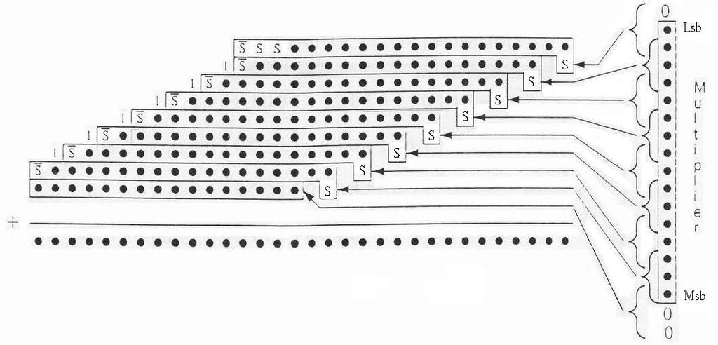
102 ddition of 8 binary numbers using the Wallace tree principal 2
103 3
104 4
105 FINISH A EGIN CLK RESET MULT32 one COUNTER2 INVERTER CLR RESULT 32 Adder AN_2 CLK 37 Q EN LAST_RESULT START CLR REGSTER37 5
106 augh-wooley two's complement multiplier: a4b' a4b' ab a3b a2b ab a3b FA FA a2b FA ab FA ab a4b2' a3b2 a2b2 ab2 FA FA FA FA ab2 a4b3' FA FA FA a3b3 a2b3 ab3 FA ab3 a4' b4' FA a4b4 FA a3'b4 FA a2'b4 FA a'b4 FA a'b4 a4 FA FA FA FA FA FA b The schematic logic circuit diagram of a 5-by-5 augh-wooley two s complement array multiplier 6
107 a 4 a 3 a 2 a a b 4 b 3 b 2 b b A a 4b ' a 3b a 2b a b a b a 4b ' a 3b a 2b a b a b a 4b 2' a 3b 2 a 2b 2 a b 2 a b 2 a 4b 4 a 4b 3' a 3b 3 a 2b 3 a b 3 a b 3 a 4' a 3'b 4 a 2'b 4 a 'b 4 a 'b 4 b 4' a 4 b 4 p9 p8 p7 p6 p5 p4 p3 p2 p p =3 = -5 = -5 =3 = -65 = -65 =3 = 5 = -3 = -5 = 65 = 65 7
108 Cluster Multipliers ivide the multiplier into smaller multipliers 8
109 Cluster Multipliers Multiplier Multiplicand A8~A7 A3~A 8~7 3~ bit Latch 8-bit Latch 8-bit Latch 8-bit Latch 4-bit Multiplier CLK 4-bit Multiplier CLK 4-bit Multiplier CLK 4-bit Multiplier CLK The circuit used to generate the enable signal /CLR 8-bit Latch EN3 EN2 EN EN CLK /CLR 8-bit Latch CLK /CLR 8-bit Latch CLK /CLR 8-bit Latch CLK Final Addition Stage bit cluster low power multiplier
110 Cluster Multipliers ividing the multiplication circuit into clusters (blocks) of smaller multipliers Applying clock gating techniques to disable the blocks that are producing a zero result. Features Low ower (claims 3.4 % savings)
111 Multiplexer-ased Array Multipliers Z 4 Z 3 Z 2 Z Z 4 Z 3 Z 2 Z j 2 Z 4 2 Z 3 3 Z 4 xjyj n j x j y j 2 2 j n j Z j 2 j Z j x jyj j y j j j j 2...
112 Multiplexer-ased Array Multipliers Two types of cells: Cell : produce the terms Z ij 2 j carry save adder array and includes a full adder of Cell 2: produce the terms x j y j 2 j and includes a full adder of carry save adder array 2
113 Multiplexer-ased Array Multipliers Characteristics Faster than Modified ooth Unlike ooth, does not require encoding logic Requires approximately N 2 /2 cells Has a zigzag shape, thus not layout-friendly 3
114 Multiplexer-ased Array Multipliers Improvement More rectangular layout Save up to 4 percent area without penalties Outperforms the modified ooth multiplier in both speed and power by 3% to 26% 4
115 Gray-Encoded Array Multiplier ec Hyb ec Hyb ec Hyb ec Hyb s complement Hybrid Coding Having a single bit different for consecutive values Reducing the number of transitions, and thus power ( for highly correlated streams ). 5
116 Gray-Encoded Array Multiplier An 8-bit wide 2 s complement radix-4 array multiplier 6
117 Gray-Encoded Array Multiplier Characteristics Uses gray code to reduce the switching activity of multiplier Saves 45.6% power than Modified ooth Uses greater area(26.4% ) than Modified ooth 7
118 Ultra-high Speed arallel Multiplier How to ultra-high speed? ased on Modified ooth Algorithm and Tree Structure (Column compress) Chooses efficient counters (3:2 and 5:3) Uses the new compressor (faster 2% ) Uses First artial product Addition (FA) Algorithm (reducing the bits of CLA by 5%) 8

119 Ultra-high Speed arallel Multiplier ivide into 3 rows or 5 rows only (most efficient). Calculate the partial products as soon as possible. The final CLA is only 6-bit instead of 32-bit. Calculation process using parallel counter in case of 6x6 ---Totally reduce delay by about 3% 9
120 ULLRLF Multiplier ULLRLF stands for Upper/Lower Left-to- Right Leapfrog. Combine the following techniques: Signal flow optimization in [3:2] adder array for partial product reduction, Left-to-right leapfrog (LRLF) signal flow, Splitting of the reduction array into upper/lower parts. 2
121 ULLRLF Multiplier ij is always connected to pin A Sin/Cin are connected to /C, most Sin signals are connected to C ) Signal flow optimization in [3:2] adder array -- For n = 32, the delay is reduced by 3 percent. -- The power is saved also. 2
122 ULLRLF Multiplier The sum signals skip over alternate rows. 2) Left-to-Right Leapfrog (LRLF) Structure -- The delay of signals is more balanceable. -- Low power. 22
123 ULLRLF Multiplier Only n2 bits 3) Upper/Lower Split Structure -- The long path of data path be broken into parallel short paths, there would be a saving in power. -- The delay of artial roducts Reduction is reduced. 23

124 ULLRLF Multiplier ULLRLF multipliers have less power than optimized tree multipliers for n 32 while keeping similar delay and area. With more regularity and inherently shorter interconnects, the ULLRLF structure presents a competitive alternative to tree structures. Floorplan of ULLRLF (n = 32) 24
125 Signed Array Multiplier A3 A3 A2 A A A3 A3 A2 A A 2 One stage of carry save adder A3 A3 A29 A A FA FA FA FA HA 3 A3 A3 A29 A28 A A FA FA FA FA FA HA STAGE 4 TO 3 (Each stage includes 32 AN gates, 3 full adders, half adder and NOT gate) 3 A3 A3 A A FA FA FA HA HA 32-bit carry look ahead adder *32-it Array Multiplier for Signed Number 25
126 Unsigned Array Multiplier A3 A3 A2 A A A3 A3 A2 A A 2 One stage of carry save adder A3 A3 A29 A A HA FA FA FA HA 3 A3 A3 A29 A28 A A FA FA FA FA FA HA STAGE 4 TO 3 (Each stage includes 32 AN gates, 3 full adders and half adder) 3 A3 A3 A A FA FA FA HA 32-bit carry look ahead adder *32-it Array Multiplier for Unsigned Number 26
127 Signed Modified ooth Multiplier E... E E... 6 rows of partial products E... E... E... E... E... E... E... E... E... E... E... E... E. E...S.... E..S... E = The inversion of sign bit in each row S = the i bit in the three encoded bits 32*32-bit ooth Multiplier for Signed Number { { { { { { { { { { { { { { { {... M u l t I p l i e r LS i- i MS 27
128 Signed Modified ooth Multiplier A3 A3 SEL A3 SEL A4 A3 A2 A A SEL SEL SEL SEL SEL SEL [] 2[] INVERT ooth Encoder [:] One stage A3 A3 A3 A29 A28 SEL SEL SEL SEL A2 A A SEL SEL SEL SEL [] 2[] INVERT ooth Encoder [3:] HA FA HA HA HA HA HA A3 A3 A3 A29 A28 A27 A26 SEL SEL SEL SEL SEL SEL A A SEL SEL SEL INVERT2 [2] 2[2] INVERT2 ooth Encoder [5:3] HA FA FA FA FA FA FA FA STAGE 3 TO 5 (Each stage includes 33 selectors, 3 full adders, half adder and NOT gate) INVERT n [n] 2[n] INVERT n ooth Encoder [3:5] INVERT INVERT 64-bit carry look ahead adder *32-it Modified ooth Multiplier for Signed Number 28
129 Unsigned Modified ooth Multiplier S'... S' S'... 7 rows of partial products S'... S'... S'... S'... S'... S'... S'... S'... S'... S'... S'... S'... S'. S'...S......S S = the i bit in the three encoded bits S' = The inversion of S 32*32-bit ooth Multiplier for unsigned Number { { { { { { { { { { { { { { { { {... i- i M u l t i p l i e r LS MS 29
130 Unsigned Modified ooth Multiplier S[] A3 SEL_ EN A3 SEL A4 A3 A2 A SEL SEL SEL SEL SEL A SEL_ EN [] 2[] S[] ooth Encoder [:] One stage S[] A3 A3 A29 A28 SEL_ EN SEL SEL SEL A2 A SEL SEL SEL A SEL_ EN [] 2[] S[] ooth Encoder [3:] HA FA HA HA HA HA HA HA S[2] A3 A3 A29 A28 A27 A26 SEL_ EN SEL SEL SEL SEL SEL A SEL A SEL SEL_ EN [2] 2[2] S[2] ooth Encoder [5:3] S[2] HA FA FA FA FA FA FA FA FA STAGE 3 TO 5 (Each stage includes 33 selectors, 32 full adders, half adder and NOT gate) S[i] [i] 2[i] S [i] ooth Encoder [i, I, i-] A3 A3 A29 SEL_ EN SEL SEL A SEL A SEL SEL_ EN [6] 2[6] S[6] ooth Encoder [3] S6 HA FA FA FA FA FA S[] S[] 64-bit carry look ahead adder *32-it Modified ooth Multiplier for Unsigned Number 3
131 Wallace Tree multipliers A[3:] [3:] 32 partial products added in Wallace Tree Adder C[63:] S[63:] 64-bit Carry Look-ahead Adder [63:] 3
132 Wallace Tree multipliers... Use the 3:2 counters and 2:2 counters Number of levels of = log (32/2) / log (3/2) 8 Irregular structure Fast Input: Output:... Carry 2:2 counter Sum... 3:2 counter Sum Carry
133 Wallace Tree multipliers A63... A Carry ropagate/generate unit Cin G63... G G63-G G7-G 8-it CLA 8-it CLA 8-it CLA 8-it CLA 8-it CLA 8-it CLA 8-it CLA 8-it CLA 2-level hierarchical C63-C56 M7 C56 GM7 C55-C48 C47-C4 C39-C32 C3-C24 C23-C6 C5-C8 M6 M5 M4 M3 M2 M C48 C4 C24 C6 GM6 GM5 GM4 GM3 GM2 GM C8 M GM C7-C 8-it CLA C63... C 64-it Summation Unit C64 S63... S 64-it Carry Look Ahead Adder 33
134 Modified ooth-wallace Tree Multipliers 34
135 Use the 3:2 counters and 2:2 counters Number of levels of = log (6/2) / log (3/2) 6 Irregular structure Fast Less area Modified ooth-wallace Tree Multipliers Rearrage ot Matrix of ooth-wallace Multiplier for Signed Number 35
136 Twin pipe serial-parallel multipliers A3 A3 A A arallel in serial out shift registers Serial in parallel out shift registers bit twin pipe serial-parallel multiplier unit arallel in serial out shift registers Serial in parallel out shift registers Result_ready Load/Shift Reset Clock Sign lock diagram of 32*32-bit signed twin pipe serial-parallel multiplier with serial/parallel conversion logic 36
137 Signed twin pipe serial-parallel multipliers Even data bits on rising clock A3 A3 A... 2 reset rising_edge FA FA falling_edge FA HA Even product Repeat 28 units more MU roduct FA FA FA HA Clock Odd data bits on rising clock... 3 reset Odd product A3 A3 A Sign Reset Clock 32*32-bit twin pipe serial-parallel multiplier for signed number Sign control line and the sign-change hardware 37
138 Unsigned twin pipe serial-parallel multipliers Even data bits on rising clock A3 A3 A... 2 reset rising_edge HA FA falling_edge FA HA Even product Repeat 28 units more MU roduct HA FA FA HA Clock Odd data bits on rising clock... 3 reset Odd product A3 A3 A Reset Clock 32*32 bit twin pipe serial-parallel multiplier for unsigned number on t need the Sign control line and the sign-change hardware 38
EE878 Special Topics in VLSI. Computer Arithmetic for Digital Signal Processing
 EE878 Special Topics in VLSI Computer Arithmetic for Digital Signal Processing Part 6c High-Speed Multiplication - III Spring 2017 Koren Part.6c.1 Array Multipliers The two basic operations - generation
Digital Computer Arithmetic
 Digital Computer Arithmetic Part 6 High-Speed Multiplication Soo-Ik Chae Spring 2010 Koren Chap.6.1 Speeding Up Multiplication Multiplication involves 2 basic operations generation of partial products
UNIVERSITY OF MASSACHUSETTS Dept. of Electrical & Computer Engineering. Digital Computer Arithmetic ECE 666
 UNIVERSITY OF MASSACHUSETTS Dept. of Electrical & Computer Engineering Digital Computer Arithmetic ECE 666 Part 6c High-Speed Multiplication - III Israel Koren Fall 2010 ECE666/Koren Part.6c.1 Array Multipliers
Partial product generation. Multiplication. TSTE18 Digital Arithmetic. Seminar 4. Multiplication. yj2 j = xi2 i M
 TSTE8 igital Arithmetic Seminar 4 Oscar Gustafsson Multiplication Multiplication can typically be separated into three sub-problems Generating partial products Adding the partial products using a redundant
EE878 Special Topics in VLSI. Computer Arithmetic for Digital Signal Processing
 EE878 Special Topics in VLSI Computer Arithmetic for Digital Signal Processing Part 6b High-Speed Multiplication - II Spring 2017 Koren Part.6b.1 Accumulating the Partial Products After generating partial
Area Efficient, Low Power Array Multiplier for Signed and Unsigned Number. Chapter 3
 Area Efficient, Low Power Array Multiplier for Signed and Unsigned Number Chapter 3 Area Efficient, Low Power Array Multiplier for Signed and Unsigned Number Chapter 3 3.1 Introduction The various sections
UNIVERSITY OF MASSACHUSETTS Dept. of Electrical & Computer Engineering. Digital Computer Arithmetic ECE 666
 UNIVERSITY OF MASSACHUSETTS Dept. of Electrical & Computer Engineering Digital Computer Arithmetic ECE 666 Part 6b High-Speed Multiplication - II Israel Koren ECE666/Koren Part.6b.1 Accumulating the Partial
An Efficient Fused Add Multiplier With MWT Multiplier And Spanning Tree Adder
 An Efficient Fused Add Multiplier With MWT Multiplier And Spanning Tree Adder 1.M.Megha,M.Tech (VLSI&ES),2. Nataraj, M.Tech (VLSI&ES), Assistant Professor, 1,2. ECE Department,ST.MARY S College of Engineering
Implementation of Efficient Modified Booth Recoder for Fused Sum-Product Operator
 Implementation of Efficient Modified Booth Recoder for Fused Sum-Product Operator A.Sindhu 1, K.PriyaMeenakshi 2 PG Student [VLSI], Dept. of ECE, Muthayammal Engineering College, Rasipuram, Tamil Nadu,
A New Architecture for 2 s Complement Gray Encoded Array Multiplier
 A New Architecture for s Complement Gray Encoded Array Multiplier Eduardo Costa Sergio Bampi José Monteiro UCPel, Pelotas, Brazil UFRGS, P. Alegre, Brazil IST/INESC, Lisboa, Portugal ecosta@atlas.ucpel.tche.br
ECE 341 Midterm Exam
 ECE 341 Midterm Exam Time allowed: 90 minutes Total Points: 75 Points Scored: Name: Problem No. 1 (10 points) For each of the following statements, indicate whether the statement is TRUE or FALSE: (a)
Jan Rabaey Homework # 7 Solutions EECS141
 UNIVERSITY OF CALIFORNIA College of Engineering Department of Electrical Engineering and Computer Sciences Last modified on March 30, 2004 by Gang Zhou (zgang@eecs.berkeley.edu) Jan Rabaey Homework # 7
One and a half hours. Section A is COMPULSORY UNIVERSITY OF MANCHESTER SCHOOL OF COMPUTER SCIENCE
 One and a half hours Section A is COMPULSORY UNIVERSITY OF MANCHESTER SCHOOL OF COMPUTER SCIENCE Fundamentals of Computer Engineering Date: Thursday 21st January 2016 Time: 14:00-15:30 Answer BOTH Questions
ECE 341 Midterm Exam
 ECE 341 Midterm Exam Time allowed: 75 minutes Total Points: 75 Points Scored: Name: Problem No. 1 (8 points) For each of the following statements, indicate whether the statement is TRUE or FALSE: (a) A
EECS Components and Design Techniques for Digital Systems. Lec 20 RTL Design Optimization 11/6/2007
 EECS 5 - Components and Design Techniques for Digital Systems Lec 2 RTL Design Optimization /6/27 Shauki Elassaad Electrical Engineering and Computer Sciences University of California, Berkeley Slides
Binary Multiplication
 inary Multiplication The key to multiplication was memorizing a digit-by-digit table Everything else was just adding 2 3 4 5 6 7 8 9 2 3 4 5 6 7 8 9 2 2 4 6 8 2 4 6 8 3 3 6 9 2 5 8 2 24 27 + You ve got
Digital Fundamentals. Lab 6 2 s Complement / Digital Calculator
 Richland College Engineering Technology Rev. 0. Donham Rev. 1 (7/2003) J. Horne Rev. 2 (1/2008) J. radbury Digital Fundamentals CETT 1425 Lab 6 2 s Complement / Digital Calculator Name: Date: Objectives:
EE 109L Review. Name: Solutions
 EE 9L Review Name: Solutions Closed Book / Score:. Short Answer (6 pts.) a. Storing temporary values in (memory / registers) is preferred due to the (increased / decreased) access time. b. True / False:
ENEE245 Digital Circuits and Systems Lab Manual
 ENEE245 Digital Circuits and Systems Lab Manual Department of Engineering, Physical & Computer Sciences Montgomery College Modified Fall 2017 Copyright Prof. Lan Xiang (Do not distribute without permission)
Microcomputers. Outline. Number Systems and Digital Logic Review
 Microcomputers Number Systems and Digital Logic Review Lecture 1-1 Outline Number systems and formats Common number systems Base Conversion Integer representation Signed integer representation Binary coded
IMPLEMENTATION OF TWIN PRECISION TECHNIQUE FOR MULTIPLICATION
 IMPLEMENTATION OF TWIN PRECISION TECHNIQUE FOR MULTIPLICATION SUNITH KUMAR BANDI #1, M.VINODH KUMAR *2 # ECE department, M.V.G.R College of Engineering, Vizianagaram, Andhra Pradesh, INDIA. 1 sunithjc@gmail.com
Design and Implementation of Signed, Rounded and Truncated Multipliers using Modified Booth Algorithm for Dsp Systems.
 Design and Implementation of Signed, Rounded and Truncated Multipliers using Modified Booth Algorithm for Dsp Systems. K. Ram Prakash 1, A.V.Sanju 2 1 Professor, 2 PG scholar, Department of Electronics
Digital Circuit Design and Language. Datapath Design. Chang, Ik Joon Kyunghee University
 Digital Circuit Design and Language Datapath Design Chang, Ik Joon Kyunghee University Typical Synchronous Design + Control Section : Finite State Machine + Data Section: Adder, Multiplier, Shift Register
Federal Urdu University of Arts, Science and Technology, Islamabad VLSI SYSTEM DESIGN. Prepared By: Engr. Yousaf Hameed.
 VLSI SYSTEM DESIGN Prepared By: Engr. Yousaf Hameed Lab Engineer BASIC ELECTRICAL & DIGITAL SYSTEMS LAB DEPARTMENT OF ELECTRICAL ENGINEERING VLSI System Design 1 LAB 01 Schematic Introduction to DSCH and
Effective Improvement of Carry save Adder
 Effective Improvement of Carry save Adder K.Nandini 1, A.Padmavathi 1, K.Pavithra 1, M.Selva Priya 1, Dr. P. Nithiyanantham 2 1 UG scholars, Department of Electronics, Jay Shriram Group of Institutions,
Array Multipliers. Figure 6.9 The partial products generated in a 5 x 5 multiplication. Sec. 6.5
 Sec. 6.5 Array Multipliers I'r) 1'8 P7 p6 PS f'4 1'3 1'2 1' 1 "0 Figure 6.9 The partial products generated in a 5 x 5 multiplication. called itemrive arrc.ly multipliers or simply cirruy m~illil>liers.
CS 5803 Introduction to High Performance Computer Architecture: Arithmetic Logic Unit. A.R. Hurson 323 CS Building, Missouri S&T
 CS 5803 Introduction to High Performance Computer Architecture: Arithmetic Logic Unit A.R. Hurson 323 CS Building, Missouri S&T hurson@mst.edu 1 Outline Motivation Design of a simple ALU How to design
Why Should I Learn This Language? VLSI HDL. Verilog-2
 Verilog Why Should I Learn This Language? VLSI HDL Verilog-2 Different Levels of Abstraction Algorithmic the function of the system RTL the data flow the control signals the storage element and clock Gate
University of Toronto Faculty of Applied Science and Engineering Edward S. Rogers Sr. Department of Electrical and Computer Engineering
 University of Toronto Faculty of Applied Science and Engineering Edward S. Rogers Sr. Department of Electrical and Computer Engineering Final Examination ECE 241F - Digital Systems Examiners: S. Brown,
ENEE 245 Lab 1 Report Rubrics
 ENEE 4 Lab 1 Report Rubrics Design Clearly state the design requirements Derive the minimum SOP Show the circuit implementation. Draw logic diagram and wiring diagram neatly Label all the diagrams/tables
Overview. EECS Components and Design Techniques for Digital Systems. Lec 16 Arithmetic II (Multiplication) Computer Number Systems.
 Computer Number Systems.") Overview EE 15 - omponents and Design Techniques for Digital ystems Lec 16 Arithmetic II (Multiplication) Review of Addition Overflow Multiplication Further adder optimizations for multiplication LA in
Overview EE 15 - omponents and Design Techniques for Digital ystems Lec 16 Arithmetic II (Multiplication) Review of Addition Overflow Multiplication Further adder optimizations for multiplication LA in
Computer Arithmetic Multiplication & Shift Chapter 3.4 EEC170 FQ 2005
 Computer Arithmetic Multiplication & Shift Chapter 3.4 EEC170 FQ 200 Multiply We will start with unsigned multiply and contrast how humans and computers multiply Layout 8-bit 8 Pipelined Multiplier 1 2
Boolean Unit (The obvious way)
") oolean Unit (The obvious way) It is simple to build up a oolean unit using primitive gates and a mux to select the function. Since there is no interconnection between bits, this unit can be simply replicated
oolean Unit (The obvious way) It is simple to build up a oolean unit using primitive gates and a mux to select the function. Since there is no interconnection between bits, this unit can be simply replicated
Injntu.com Injntu.com Injntu.com R16
 1. a) What are the three methods of obtaining the 2 s complement of a given binary (3M) number? b) What do you mean by K-map? Name it advantages and disadvantages. (3M) c) Distinguish between a half-adder
ENEE245 Digital Circuits and Systems Lab Manual
 ENEE245 Digital Circuits and Systems Lab Manual Department of Engineering, Physical & Computer Sciences Montgomery College Version 1.1 Copyright Prof. Lan Xiang (Do not distribute without permission) 1
Combinational Circuit Design
 Modeling Combinational Circuits with Verilog Prof. Chien-Nan Liu TEL: 3-42275 ext:34534 Email: jimmy@ee.ncu.edu.tw 3- Combinational Circuit Design Outputs are functions of inputs inputs Combinational Circuit
UNIVERSITY OF TORONTO FACULTY OF APPLIED SCIENCE AN:p ENGINEERING. ECE241F - Digital Syst~ms Final Examination
 ~.. UNIVERSITY OF TORONTO FACULTY OF APPLIED SCIENCE AN:p ENGINEERING ECE241F - Digital Syst~ms Final Examination December 19, 2017, 2:00pm-4:30pm Duration: 2.5 hours Examiners: P. Anderson, P. Chow and
Sum to Modified Booth Recoding Techniques For Efficient Design of the Fused Add-Multiply Operator
 Sum to Modified Booth Recoding Techniques For Efficient Design of the Fused Add-Multiply Operator D.S. Vanaja 1, S. Sandeep 2 1 M. Tech scholar in VLSI System Design, Department of ECE, Sri VenkatesaPerumal
Learning Outcomes. Spiral 2-2. Digital System Design DATAPATH COMPONENTS
 2-2. 2-2.2 Learning Outcomes piral 2-2 Arithmetic Components and Their Efficient Implementations I understand the control inputs to counters I can design logic to control the inputs of counters to create
ECE 645: Lecture 1. Basic Adders and Counters. Implementation of Adders in FPGAs
 ECE 645: Lecture Basic Adders and Counters Implementation of Adders in FPGAs Required Reading Behrooz Parhami, Computer Arithmetic: Algorithms and Hardware Design Chapter 5, Basic Addition and Counting,
Binary Arithmetic. Daniel Sanchez Computer Science & Artificial Intelligence Lab M.I.T.
 Binary Arithmetic Daniel Sanchez Computer Science & Artificial Intelligence Lab M.I.T. MIT 6.004 Fall 2018 Reminder: Encoding Positive Integers Bit i in a binary representation (in right-to-left order)
Control Unit: Binary Multiplier. Arturo Díaz-Pérez Departamento de Computación Laboratorio de Tecnologías de Información CINVESTAV-IPN
 Control Unit: Binary Multiplier Arturo Díaz-Pérez Departamento de Computación Laboratorio de Tecnologías de Información CINVESTAV-IPN Example: Binary Multiplier Two versions Hardwired control Microprogrammed
ECE331: Hardware Organization and Design
 ECE331: Hardware Organization and Design Lecture 9: Binary Addition & Multiplication Adapted from Computer Organization and Design, Patterson & Hennessy, UCB Pop Quiz! Using 4 bits signed integer notation:
VARUN AGGARWAL
 ECE 645 PROJECT SPECIFICATION -------------- Design A Microprocessor Functional Unit Able To Perform Multiplication & Division Professor: Students: KRIS GAJ LUU PHAM VARUN AGGARWAL GMU Mar. 2002 CONTENTS
Arithmetic Circuits. Nurul Hazlina Adder 2. Multiplier 3. Arithmetic Logic Unit (ALU) 4. HDL for Arithmetic Circuit
 4. HDL for Arithmetic Circuit") Nurul Hazlina 1 1. Adder 2. Multiplier 3. Arithmetic Logic Unit (ALU) 4. HDL for Arithmetic Circuit Nurul Hazlina 2 Introduction 1. Digital circuits are frequently used for arithmetic operations 2. Fundamental
Nurul Hazlina 1 1. Adder 2. Multiplier 3. Arithmetic Logic Unit (ALU) 4. HDL for Arithmetic Circuit Nurul Hazlina 2 Introduction 1. Digital circuits are frequently used for arithmetic operations 2. Fundamental
Chapter 5 Registers & Counters
 University of Wisconsin - Madison ECE/Comp Sci 352 Digital Systems Fundamentals Kewal K. Saluja and Yu Hen Hu Spring 2002 Chapter 5 Registers & Counters Originals by: Charles R. Kime Modified for course
Fundamentals of Computer Systems
 Fundamentals of Computer Systems Combinational Logic Martha. Kim Columbia University Spring 6 / Combinational Circuits Combinational circuits are stateless. Their output is a function only of the current
Arithmetic Logic Unit. Digital Computer Design
 Arithmetic Logic Unit Digital Computer Design Arithmetic Circuits Arithmetic circuits are the central building blocks of computers. Computers and digital logic perform many arithmetic functions: addition,
ECE 341. Lecture # 7
 ECE 34 Lecture # 7 Instructor: Zeshan Chishti zeshan@pdx.edu October 2, 24 Portland State University Lecture Topics Multiplication of Unsigned Numbers Sequential Circuit Multiplier Multiplication of Signed
Today. Comments about assignment Max 1/T (skew = 0) Max clock skew? Comments about assignment 3 ASICs and Programmable logic Others courses
 Max clock skew? Comments about assignment 3 ASICs and Programmable logic Others courses") Today Comments about assignment 3-43 Comments about assignment 3 ASICs and Programmable logic Others courses octor Per should show up in the end of the lecture Mealy machines can not be coded in a single
Today Comments about assignment 3-43 Comments about assignment 3 ASICs and Programmable logic Others courses octor Per should show up in the end of the lecture Mealy machines can not be coded in a single
University of Illinois at Chicago. Lecture Notes # 10
 ECE 366 Computer Architecture Instructor: Shantanu Dutt Department of Electrical and Computer Engineering University of Illinois at Chicago Lecture otes # 0 COMPUTER ARITHMETIC: Integer Addition and Multiplication
Computer Architecture: Part III. First Semester 2013 Department of Computer Science Faculty of Science Chiang Mai University
 Computer Architecture: Part III First Semester 2013 Department of Computer Science Faculty of Science Chiang Mai University Outline Decoders Multiplexers Registers Shift Registers Binary Counters Memory
A New Pipelined Array Architecture for Signed Multiplication
 A New Pipelined Array Architecture for Signed Multiplication Eduardo Costa, Sergio Bampi José Monteiro UCPel, Pelotas, Brazil UFRGS, P. Alegre, Brazil IST/INESC, Lisboa, Portugal ecosta@ucpel.tche.br bampi@inf.ufrgs.br
3 Designing Digital Systems with Algorithmic State Machine Charts
 3 Designing with Algorithmic State Machine Charts An ASM chart is a method of describing the sequential operations of a digital system which has to implement an algorithm. An algorithm is a well defined
High Speed Special Function Unit for Graphics Processing Unit
 High Speed Special Function Unit for Graphics Processing Unit Abd-Elrahman G. Qoutb 1, Abdullah M. El-Gunidy 1, Mohammed F. Tolba 1, and Magdy A. El-Moursy 2 1 Electrical Engineering Department, Fayoum
HIGH PERFORMANCE FUSED ADD MULTIPLY OPERATOR
 HIGH PERFORMANCE FUSED ADD MULTIPLY OPERATOR R. Alwin [1] S. Anbu Vallal [2] I. Angel [3] B. Benhar Silvan [4] V. Jai Ganesh [5] 1 Assistant Professor, 2,3,4,5 Student Members Department of Electronics
Computer Architecture, IFE CS and T&CS, 4 th sem. Fast Adders
 Fast Adders Adders Overview (not complete) 1-bit Adders CPA (Carry Propagate Adders) 3-operand Multi-operand Adders Half Adder HA Adder Array RCA Full Adder FA CSA CSKA CSLA CLA Bit Counter (m,k) Adder
ECE 30 Introduction to Computer Engineering
 ECE 30 Introduction to Computer Engineering Study Problems, Set #6 Spring 2015 1. With x = 1111 1111 1111 1111 1011 0011 0101 0011 2 and y = 0000 0000 0000 0000 0000 0010 1101 0111 2 representing two s
Learning Outcomes. Spiral 2 2. Digital System Design DATAPATH COMPONENTS
 2-2. 2-2.2 Learning Outcomes piral 2 2 Arithmetic Components and Their Efficient Implementations I know how to combine overflow and subtraction results to determine comparison results of both signed and
EE 109L Final Review
 EE 09L Final Review Name: Closed Book / Score:. Short Answer (6 pts.) a. Storing temporary values in (memory / registers) is preferred due to the (increased / decreased) access time. b. True / False: A
Verilog Tutorial. Introduction. T. A.: Hsueh-Yi Lin. 2008/3/12 VLSI Digital Signal Processing 2
 Verilog Tutorial T. A.: Hsueh-Yi Lin Introduction 2008/3/12 VLSI Digital Signal Processing 2 Verilog: A common language for industry HDL is a common way for hardware design Verilog VHDL Verilog is widely
ECE 341. Lecture # 6
 ECE 34 Lecture # 6 Instructor: Zeshan Chishti zeshan@pdx.edu October 5, 24 Portland State University Lecture Topics Design of Fast Adders Carry Looakahead Adders (CLA) Blocked Carry-Lookahead Adders Multiplication
Luleå University of Technology Kurskod SMD152 Datum Skrivtid
 Luleå University of Technology Kurskod SMD152 Datum 2003-10-24 Skrivtid 9.00 13.00 1 Manual synthesis (10 p, 2 p each) Here you are given five different VHDL models. Your task is to draw the schematics
JOURNAL OF INTERNATIONAL ACADEMIC RESEARCH FOR MULTIDISCIPLINARY Impact Factor 1.393, ISSN: , Volume 2, Issue 7, August 2014
 DESIGN OF HIGH SPEED BOOTH ENCODED MULTIPLIER PRAVEENA KAKARLA* *Assistant Professor, Dept. of ECONE, Sree Vidyanikethan Engineering College, A.P., India ABSTRACT This paper presents the design and implementation
Digital Logic & Computer Design CS Professor Dan Moldovan Spring 2010
 Digital Logic & Computer Design CS 434 Professor Dan Moldovan Spring 2 Copyright 27 Elsevier 5- Chapter 5 :: Digital Building Blocks Digital Design and Computer Architecture David Money Harris and Sarah
Clocked Sequential System Design. Multiply Example
 Clocked Sequential System Design Example 1 Multipliers (Gradeschool, Modified Gradeschool) Multiply Example (185) (215) 00000000 00000000 ------ 1001101101011111 (39775) 1 0000000000000000
OPTIMIZING THE POWER USING FUSED ADD MULTIPLIER
 Available Online at www.ijcsmc.com International Journal of Computer Science and Mobile Computing A Monthly Journal of Computer Science and Information Technology IJCSMC, Vol. 3, Issue. 11, November 2014,
ECE 341 Midterm Exam
 ECE 341 Midterm Exam Time allowed: 90 minutes Total Points: 75 Points Scored: Name: Problem No. 1 (11 points) For parts (a) through (d), indicate whether the statement is TRUE or FALSE. For parts (e) and
Music. Numbers correspond to course weeks EULA ESE150 Spring click OK Based on slides DeHon 1. !
 MIC Lecture #7 Digital Logic Music 1 Numbers correspond to course weeks sample EULA D/A 10101001101 click OK Based on slides 2009--2018 speaker MP Player / iphone / Droid DeHon 1 2 A/D domain conversion
Chapter 5. Digital Design and Computer Architecture, 2 nd Edition. David Money Harris and Sarah L. Harris. Chapter 5 <1>
 Chapter 5 Digital Design and Computer Architecture, 2 nd Edition David Money Harris and Sarah L. Harris Chapter 5 Chapter 5 :: Topics Introduction Arithmetic Circuits umber Systems Sequential Building
International Journal of Computer Trends and Technology (IJCTT) volume 17 Number 5 Nov 2014 LowPower32-Bit DADDA Multipleir
 volume 17 Number 5 Nov 2014 LowPower32-Bit DADDA Multipleir") LowPower32-Bit DADDA Multipleir K.N.V.S.Vijaya Lakshmi 1, D.R.Sandeep 2 1 PG Scholar& ECE Department&JNTU Kakinada University Sri Vasavi Engineering College, Tadepalligudem, Andhra Pradesh, India 2 AssosciateProfessor&
LowPower32-Bit DADDA Multipleir K.N.V.S.Vijaya Lakshmi 1, D.R.Sandeep 2 1 PG Scholar& ECE Department&JNTU Kakinada University Sri Vasavi Engineering College, Tadepalligudem, Andhra Pradesh, India 2 AssosciateProfessor&
1. Prove that if you have tri-state buffers and inverters, you can build any combinational logic circuit. [4]
![1. Prove that if you have tri-state buffers and inverters, you can build any combinational logic circuit. [4]](/thumbs/81/83055464.jpg "1. Prove that if you have tri-state buffers and inverters, you can build any combinational logic circuit. [4]") HW 3 Answer Key 1. Prove that if you have tri-state buffers and inverters, you can build any combinational logic circuit. [4] You can build a NAND gate from tri-state buffers and inverters and thus you
HW 3 Answer Key 1. Prove that if you have tri-state buffers and inverters, you can build any combinational logic circuit. [4] You can build a NAND gate from tri-state buffers and inverters and thus you
CMPT 250 : Week 3 (Sept 19 to Sept 26)
") CMPT 250 : Week 3 (Sept 19 to Sept 26) 1. DESIGN FROM FINITE STATE MACHINES (Continued) 1.1. ONE FLIP-FLOP PER STATE METHOD From a state diagram specification, a sequencer can be constructed using the
CMPT 250 : Week 3 (Sept 19 to Sept 26) 1. DESIGN FROM FINITE STATE MACHINES (Continued) 1.1. ONE FLIP-FLOP PER STATE METHOD From a state diagram specification, a sequencer can be constructed using the
Learning Outcomes. Spiral 2 2. Digital System Design DATAPATH COMPONENTS
 2-2. 2-2.2 Learning Outcomes piral 2 2 Arithmetic Components and Their Efficient Implementations I know how to combine overflow and subtraction results to determine comparison results of both signed and
UNIT-III REGISTER TRANSFER LANGUAGE AND DESIGN OF CONTROL UNIT
 UNIT-III 1 KNREDDY UNIT-III REGISTER TRANSFER LANGUAGE AND DESIGN OF CONTROL UNIT Register Transfer: Register Transfer Language Register Transfer Bus and Memory Transfers Arithmetic Micro operations Logic
Lecture 12 VHDL Synthesis
 CPE 487: Digital System Design Spring 2018 Lecture 12 VHDL Synthesis Bryan Ackland Department of Electrical and Computer Engineering Stevens Institute of Technology Hoboken, NJ 07030 1 What is Synthesis?
Computer Organization EE 3755 Midterm Examination
 Name Computer Organization EE 3755 Midterm Examination Wednesday, 30 October 2013, 8:30 9:20 CDT Alias Problem 1 Problem 2 Problem 3 Problem 4 Problem 5 Problem 6 Problem 7 Exam Total (21 pts) (15 pts)
II. MOTIVATION AND IMPLEMENTATION
 An Efficient Design of Modified Booth Recoder for Fused Add-Multiply operator Dhanalakshmi.G Applied Electronics PSN College of Engineering and Technology Tirunelveli dhanamgovind20@gmail.com Prof.V.Gopi
Topics. Midterm Finish Chapter 7
 Lecture 9 Topics Midterm Finish Chapter 7 ROM (review) Memory device in which permanent binary information is stored. Example: 32 x 8 ROM Five input lines (2 5 = 32) 32 outputs, each representing a memory
Chapter 6 ARITHMETIC FOR DIGITAL SYSTEMS
 Chapter 6 ARITHMETIC FOR DIGITAL SYSTEMS Introduction Notation Systems Principle of Generation and Propagation The bit Full Adder Enhancement Techniques for Adders Multioperand Adders Multiplication Addition
Written exam for IE1204/5 Digital Design Thursday 29/
 Written exam for IE1204/5 Digital Design Thursday 29/10 2015 9.00-13.00 General Information Examiner: Ingo Sander. Teacher: William Sandqvist phone 08-7904487 Exam text does not have to be returned when
VTU NOTES QUESTION PAPERS NEWS RESULTS FORUMS Arithmetic (a) The four possible cases Carry (b) Truth table x y
 The four possible cases Carry (b) Truth table x y") Arithmetic A basic operation in all digital computers is the addition and subtraction of two numbers They are implemented, along with the basic logic functions such as AND,OR, NOT,EX- OR in the ALU subsystem
Arithmetic A basic operation in all digital computers is the addition and subtraction of two numbers They are implemented, along with the basic logic functions such as AND,OR, NOT,EX- OR in the ALU subsystem
Analysis of Different Multiplication Algorithms & FPGA Implementation
 IOSR Journal of VLSI and Signal Processing (IOSR-JVSP) Volume 4, Issue 2, Ver. I (Mar-Apr. 2014), PP 29-35 e-issn: 2319 4200, p-issn No. : 2319 4197 Analysis of Different Multiplication Algorithms & FPGA
Figure 1 Circuit for problem 1.
 Problem : Do Shannon s expansion on A'B' + A'BC + A'BDE + AB'C'D' + AB'C'E' L A'B' = L A'B = C + DE L AB' = C'D' + C'E' = (C + DE)' L AB = Observation : (L A'B )' = (C + DE)' = C'(DE)' = C'(D' + E') =
Final Exam Solution Sunday, December 15, 10:05-12:05 PM
 Last (family) name: First (given) name: Student I.D. #: Circle section: Kim Hu Department of Electrical and Computer Engineering University of Wisconsin - Madison ECE/CS 352 Digital System Fundamentals
A novel technique for fast multiplication
 INT. J. ELECTRONICS, 1999, VOL. 86, NO. 1, 67± 77 A novel technique for fast multiplication SADIQ M. SAIT², AAMIR A. FAROOQUI GERHARD F. BECKHOFF and In this paper we present the design of a new high-speed
CPE300: Digital System Architecture and Design
 CPE300: Digital System Architecture and Design Fall 2011 MW 17:30-18:45 CBC C316 Arithmetic Unit 10122011 http://www.egr.unlv.edu/~b1morris/cpe300/ 2 Outline Recap Fixed Point Arithmetic Addition/Subtraction
Arithmetic Circuits & Multipliers
 Arithmetic Circuits & Multipliers Addition, subtraction Performance issues -- ripple carry -- carry bypass -- carry skip -- carry lookahead Multipliers Reminder: Lab #3 due tonight! Pizza Wed 6p 1 Signed
MASSACHUSETTS INSTITUTE OF TECHNOLOGY Department of Electrical Engineering and Computer Sciences
 MASSACHUSETTS INSTITUTE OF TECHNOLOGY Department of Electrical Engineering and Computer Sciences Introductory Digital Systems Lab (6.111) uiz - Spring 2004 Prof. Anantha Chandrakasan Student Name: Problem
Chapter 3: part 3 Binary Subtraction
 Chapter 3: part 3 Binary Subtraction Iterative combinational circuits Binary adders Half and full adders Ripple carry and carry lookahead adders Binary subtraction Binary adder-subtractors Signed binary
FPGA Design Challenge :Techkriti 14 Digital Design using Verilog Part 1
 FPGA Design Challenge :Techkriti 14 Digital Design using Verilog Part 1 Anurag Dwivedi Digital Design : Bottom Up Approach Basic Block - Gates Digital Design : Bottom Up Approach Gates -> Flip Flops Digital
MULTIPLICATION TECHNIQUES
 Learning Objectives EE 357 Unit 2a Multiplication Techniques Perform by hand the different methods for unsigned and signed multiplication Understand the various digital implementations of a multiplier
Contents. Chapter 9 Datapaths Page 1 of 28
 Chapter 9 Datapaths Page of 2 Contents Contents... 9 Datapaths... 2 9. General Datapath... 3 9.2 Using a General Datapath... 5 9.3 Timing Issues... 7 9.4 A More Complex General Datapath... 9 9.5 VHDL for
At the ith stage: Input: ci is the carry-in Output: si is the sum ci+1 carry-out to (i+1)st state
st state") Chapter 4 xi yi Carry in ci Sum s i Carry out c i+ At the ith stage: Input: ci is the carry-in Output: si is the sum ci+ carry-out to (i+)st state si = xi yi ci + xi yi ci + xi yi ci + xi yi ci = x i yi
Chapter 4 xi yi Carry in ci Sum s i Carry out c i+ At the ith stage: Input: ci is the carry-in Output: si is the sum ci+ carry-out to (i+)st state si = xi yi ci + xi yi ci + xi yi ci + xi yi ci = x i yi
FPGA Matrix Multiplier
 FPGA Matrix Multiplier In Hwan Baek Henri Samueli School of Engineering and Applied Science University of California Los Angeles Los Angeles, California Email: chris.inhwan.baek@gmail.com David Boeck Henri
Efficient Radix-10 Multiplication Using BCD Codes
 Efficient Radix-10 Multiplication Using BCD Codes P.Ranjith Kumar Reddy M.Tech VLSI, Department of ECE, CMR Institute of Technology. P.Navitha Assistant Professor, Department of ECE, CMR Institute of Technology.
a, b sum module add32 sum vector bus sum[31:0] sum[0] sum[31]. sum[7:0] sum sum overflow module add32_carry assign
![a, b sum module add32 sum vector bus sum[31:0] sum[0] sum[31]. sum[7:0] sum sum overflow module add32_carry assign](/thumbs/91/106466219.jpg "a, b sum module add32 sum vector bus sum[31:0] sum[0] sum[31]. sum[7:0] sum sum overflow module add32_carry assign") I hope you have completed Part 1 of the Experiment. This lecture leads you to Part 2 of the experiment and hopefully helps you with your progress to Part 2. It covers a number of topics: 1. How do we specify
I hope you have completed Part 1 of the Experiment. This lecture leads you to Part 2 of the experiment and hopefully helps you with your progress to Part 2. It covers a number of topics: 1. How do we specify
Computer Organization. Structure of a Computer. Registers. Register Transfer. Register Files. Memories
 Computer Organization Structure of a Computer Computer design as an application of digital logic design procedures Computer = processing unit + memory system Processing unit = control + Control = finite
COMP 303 Computer Architecture Lecture 6
 COMP 303 Computer Architecture Lecture 6 MULTIPLY (unsigned) Paper and pencil example (unsigned): Multiplicand 1000 = 8 Multiplier x 1001 = 9 1000 0000 0000 1000 Product 01001000 = 72 n bits x n bits =
Synthesis of Language Constructs. 5/10/04 & 5/13/04 Hardware Description Languages and Synthesis
 Synthesis of Language Constructs 1 Nets Nets declared to be input or output ports are retained Internal nets may be eliminated due to logic optimization User may force a net to exist trireg, tri0, tri1