Advanced light management techniques for building integrated PV (BIPV)
|
|
|
- Paula Bridges
- 5 years ago
- Views:
Transcription

1 Advanced light management techniques for building integrated PV (BIPV) A. Ingenito, J. C. O. Lizcano, O. Isabella, M. Zeman Delft University of Technology


![[1,3] Roadmap [1] International Technology](/docs-images/92/109839409/images/2-3.jpg "Roadmap for Photovoltaic (ITRPV), (2013) [2] A.")
 [3] Predictions for")
2 Advanced light management Roadmap for decreasing costs of c-si PV Decrease wafer cell costs [1] Wafer accounts for more than 50% of the cell costs [2] Customized PV products [1] Building integrated PV (BIPV) combining building elements and PV functionality Oskomera Solar [1,3] Roadmap [1] International Technology Roadmap for Photovoltaic (ITRPV), (2013) [2] A. Goodrich et al. SOLMAT 114, (2013) [3] Predictions for the Solar Industry in 2014, IHS Whitepaper (2013) 2

![4n 2 absorption enhancement [1] Front](/docs-images/92/109839409/images/3-1.jpg "nano-texture (RIE) 2 µm 1.0 0.8 DBR Ag (ref.")

![0 400 600 800 1000 1200 Wavelength [nm] [1]](/docs-images/92/109839409/images/3-3.jpg "A. Ingenito, O. Isabella, M.")
3 Advanced light management in c-si Experimental demonstration of upper limit 4n 2 absorption enhancement [1] Front nano-texture (RIE) 2 µm DBR Ag (ref.) Bulk c-si 20 μm Thermal SiO 2 DBR A Si [-] μm Textured BS 2 µm Wavelength [nm] [1] A. Ingenito, O. Isabella, M. Zeman, ACS Photonics, 1, 3 (2014) 3
 635 J SC (ma/cm 2 ) 40.5 FF (%) 77.0 0.6 0.4 R [-] 280 μm 0.")
![2 η (%) 19.8 0.2 Front side 0.0 0.0 300 450 600 750 900 1050 1200 Wavelength [nm] A.](/docs-images/92/109839409/images/4-1.jpg "Ingenito, O. Isabella, M. Zeman. Progress in Photovoltaics, DOI: 10.1002/pip.")
4 Advanced light management in c-si IBC c-si solar cells IBC structure EQE [-] V OC (mv) 635 J SC (ma/cm 2 ) 40.5 FF (%) R [-] 280 μm 0.2 η (%) Front side Wavelength [nm] A. Ingenito, O. Isabella, M. Zeman. Progress in Photovoltaics, DOI: /pip.2606 (2015) 4
![Advanced light management in c-si Black IBC c-si solar cells for high yield and BIPV applications [1] Black modules are highly requested for residential PV [2] [1] H.](/docs-images/92/109839409/images/5-1.jpg "Savin, P. Repo, G. von Gastrow, P. Ortega, E. Calle, M. Garín, Nature Nanotechnology, DOI: 0.1038/nnano.2015.")
5 Advanced light management in c-si Black IBC c-si solar cells for high yield and BIPV applications [1] Black modules are highly requested for residential PV [2] [1] H. Savin, P. Repo, G. von Gastrow, P. Ortega, E. Calle, M. Garín, Nature Nanotechnology, DOI: /nnano (2015) [2] Paul de Jong, Exasun, BJ-BC workshop, Freiburg, (2015) 5
6 Advanced light management Roadmap for decreasing costs of c-si PV Decrease wafer cell costs [1] Wafer accounts for more than 50% of the cell costs [2] Customized PV products [1] Building integrated PV (BIPV) combining building elements and PV functionality Oskomera Solar [1,3] Roadmap [1] International Technology Roadmap for Photovoltaic (ITRPV), (2013) [2] A. Goodrich et al. SOLMAT 114, (2013) [3] Predictions for the Solar Industry in 2014, IHS Whitepaper (2013) 6
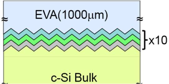
7 Optical filters (OF) as coloured coatings OF for front and/or back side coloured PV Glass EVA x 10 Glass EVA 10 x ARC ARC Emitter c-si Emitter c-si c-si BSF 10 x BSF Rear coating EVA Al Al Glass 7

8 OF s requirements and materials Exploits interference effect Based on pairs of dielectric thin-films Stronger effect with high/low refractive refractive index mismatch Several materials can be used, among the others: MgF 2 SiO 2 TiO 2 Si x N y a-si:h SiO 2 Si x N y x pairs Features Non absorbing materials in spectral range of interest o [ ] nm for Front side o [ ] nm for Back side Reflectance above 80% at desired wavelength Substrate (Glass or wafer) Protected by glass/encapsulant 8
9 OF s optical modelling 1,00 0,90 0,80 0,70 0,60 0,50 0,40 0,30 0,20 0, D Ray tracing* 0, Reflectance profile 3. Color Coordinates SunRay software by dr. R. Santbergen 9


10 Selected colours for validation SiO 2 = 100 nm Si x N y = 100 nm SiO 2 = 90 nm Si x N y = 100 nm SiO 2 = 40 nm Si x N y = 110 nm PE-CVD 10
11 Optical filters (OF) as coloured coatings OF for front and/or back side coloured PV Glass EVA x 10 Glass EVA 10 x ARC ARC Emitter c-si Emitter c-si c-si BSF 10 x BSF Rear coating EVA Al Al Glass 11
 10 x Glass EVA ARC 1.0 0.8 EQE [-] 0.")
 Coloured 0.")
12 Colour matrix (OF on glass and c-si solar cell) 10 x Glass EVA ARC EQE [-] ma/cm 2 Standard ARC (NO-OF) Coloured Wavelength [nm] 12
 Angular resilience 10 x Glass EVA ARC")
13 Colour matrix (OF on glass and c-si solar cell) Angular resilience 10 x Glass EVA ARC 13
14 Colour matrix (OF on c-si solar cell in glass) 10 x Glass EVA ARC EQE [-] ma/cm 2 Standard ARC (NO-OF) Coloured Wavelength [nm] 14
 Angular resilience 10 x Glass EVA")
15 Colour matrix (OF on c-si solar cell in glass) Angular resilience 10 x Glass EVA ARC 15
16 Passive thermal control [1] for BIPV Preliminary study Glass +20 pairs EVA ARC Emitter c-si BSF Al Potential for Passively reducing module temperature Concurrently combining colour and thermal control [1] A. P. Raman, et al., Nature, 515, (2014) 16


17 Optical filters (OF) as coloured coatings OF for front and/or back side coloured PV Glass EVA x 10 Glass EVA 10 x ARC ARC Emitter c-si Emitter c-si c-si BSF 10 x BSF Rear coating EVA Al Al Glass 17

18 Distributed Bragg Reflector (DBR) DBR can act as both back reflector (BRs) and OF High R at SiO 2 / Si interface in the weak absorption region if Si 1.0 PCB 0.8 R Sim [-] Region of weak absorption in c-si DBR λ B Wavelength [nm] A. Ingenito, O. Isabella, M. Zeman, ACS Photonics, 1, 3 (2014) 18
![Fabrication of DBR on textured surfaces 1.0 0.8 DBR R, T [-] 0.6 0.4 R 0.2 T 0.](/docs-images/92/109839409/images/19-0.jpg "0 400 600 800 1000 1200 Wavelength [nm] Co-depostion of 6 x a-si:h (80 nm) / a-sin x :H")
19 Fabrication of DBR on textured surfaces DBR R, T [-] R 0.2 T Wavelength [nm] Co-depostion of 6 x a-si:h (80 nm) / a-sin x :H (180 nm) 19
![Fabrication of DBR on textured surfaces 1.0 0.8 DBR R, T [-] 0.6 0.4 R? 0.2 R T T DBR 0.](/docs-images/92/109839409/images/20-0.jpg "0 400 600 800 1000 1200 Wavelength [nm] Co-depostion of 6 x a-si:h (80 nm) / a-sin x :H (180")
20 Fabrication of DBR on textured surfaces DBR R, T [-] R? 0.2 R T T DBR Wavelength [nm] Co-depostion of 6 x a-si:h (80 nm) / a-sin x :H (180 nm) 20

21 DBR optimization for textured surface =54.7 X= Y*sin (90 - θ) = Y*0.57 A. Ingenito, S.L. Luxembourg, P. Spinelli, J. Liu, J. C. O. Lizcano, A. Weeber, O. Isabella, M. Zeman, IEEE JPV, accepted for publication (2015) 21
22 DBR optimization for textured surface Influence of scaling factor on A Si ma / cm A Si [-] DBR 38.1 ma/cm Wavelength [nm] Wavelength [nm] A. Ingenito, S.L. Luxembourg, P. Spinelli, J. Liu, J. C. O. Lizcano, A. Weeber, O. Isabella, M. Zeman, IEEE JPV, accepted for publication (2015) 22


![7 R DBR air [-] 1.0 0.8 0.6 0.](/docs-images/92/109839409/images/23-2.jpg "4 0.8 1.0 1.2 1.5 1.7 0.8 1 1.")

23 DBR optimization for textured surface Influence of scaling factor on λ B at DBR / air interface R DBR air [-] Light 0.2 DBR Wavelength [nm] 23
![DBR (OF) as coloured coatings Application in glass/glass modules Coloured cell [1] Coloured module](/docs-images/92/109839409/images/24-0.jpg "n-pasha cell [2] [1] A. Ingenito, S.L. Luxembourg, P. Spinelli, J. Liu, J. C. O. Lizcano, A.")
![Weeber, O. Isabella, M. Zeman, IEEE JPV, accepted for publication (2015) [2] I. G. Romijn, A.](/docs-images/92/109839409/images/24-1.jpg "Gutjahr, D. Saynova, J. Anker, E.J Kossen, K. Tool. Photovoltaics International, 2013, vol. 20. pp.")
24 DBR (OF) as coloured coatings Application in glass/glass modules Coloured cell [1] Coloured module n-pasha cell [2] [1] A. Ingenito, S.L. Luxembourg, P. Spinelli, J. Liu, J. C. O. Lizcano, A. Weeber, O. Isabella, M. Zeman, IEEE JPV, accepted for publication (2015) [2] I. G. Romijn, A. Gutjahr, D. Saynova, J. Anker, E.J Kossen, K. Tool. Photovoltaics International, 2013, vol. 20. pp


25 Advanced light management for BIPV Experimental demonstration of advanced light management techniques for absorption enhancement in thin c-si absorbers Application of advanced light management for black IBC c-si solar cells with efficiency of 19.8% EQE [-] R [-] Design of OFs as colour-tuning coatings for front and/or rear side coloured PV Model validation Design and optical simulations of DBR on textured surfaces Concurrent colour and thermal control (on-going) Wavelength [nm] 25


26 Thank you! Acknowledgments: Martijn Tijssen Martijn van Sebille Stefan Luxembourg Pierpaolo Spinelli Funding: Agentschap NL
27 Outline Roadmap for decreasing the cost of c-si PV module Advanced light management techniques as possible solution to decrease LCOE Thin c-si solar cells Customized products as Building integrated PV Conclusions 2
![DBR optimization for textured surface Ray tracing simulations Parameter space: a-si:h [40:10:140] nm a-sin x :H [70:10:240]](/docs-images/92/109839409/images/28-0.jpg "nm Si SiO 2 DBR DBR = 6 x (a-si:h /a-sin x :H) [1] a-sin x :H [nm] 230 210 190 170 150 130 110 90 J PH-T = 6.")
![1 10-3 ma/cm 2 [2] Textured 70 40 60 80 100 120 140 a-si:h [nm] J ph T [ma/cm 2 ] 0.005 0.01 0.05 0.1 0.5 1.0 1.5 2.0 [1] A.](/docs-images/92/109839409/images/28-1.jpg "Ingenito, O. Isabella, M. Zeman, ACS Photonics, 1, 3, (2014) [2] J.C.O. Lizcano, MSC thesis, Optic Filters for BIPV applications (2014) 20")
28 DBR optimization for textured surface Ray tracing simulations Parameter space: a-si:h [40:10:140] nm a-sin x :H [70:10:240] nm Si SiO 2 DBR DBR = 6 x (a-si:h /a-sin x :H) [1] a-sin x :H [nm] J PH-T = ma/cm 2 [2] Textured a-si:h [nm] J ph T [ma/cm 2 ] [1] A. Ingenito, O. Isabella, M. Zeman, ACS Photonics, 1, 3, (2014) [2] J.C.O. Lizcano, MSC thesis, Optic Filters for BIPV applications (2014) 20


29 Color resilience against angle of incidence 13


30 Device level color matrix 14
31 Performance of a cell under colored glass Parameter Standard Green Yellow J PH [ma/cm 2 ] V OC [V] FF [-] iη[%]
32 Color resilience against angle of incidence 16


33 Color resilience against angle of incidence 17

 / a-sin x :H (270")
34 DBR optimization for textured surface Losses analysis 6x a-si:h (80 nm) / a-sin x :H (180 nm) Max 6x a-si:h (120 nm) / a-sin x :H (270 nm) Min 38
![DBR optimization for textured surface Influence of scaling factor on R and T 1.0 1.0 R [-] 0.8 0.6 0.4 0.8 1.0 1.2 1.5 1.7 DBR 0.8 0.6 0.4 T [-] 0.2 0.2 400 600 800 1000 1200 Wavelength [nm] 0.](/docs-images/92/109839409/images/35-0.jpg "0 400 600 800 1000 1200 Wavelength [nm] From DBR = 6 x a-si:h (80 nm) / a-sin x :H (180 nm) to scaled thicknesses A. Ingenito, S.L. Luxembourg, P. Spinelli, J. Liu, J. C. O. Lizcano, A. Weeber, O.")
35 DBR optimization for textured surface Influence of scaling factor on R and T R [-] DBR T [-] Wavelength [nm] Wavelength [nm] From DBR = 6 x a-si:h (80 nm) / a-sin x :H (180 nm) to scaled thicknesses A. Ingenito, S.L. Luxembourg, P. Spinelli, J. Liu, J. C. O. Lizcano, A. Weeber, O. Isabella, M. Zeman, IEEE JPV, accepted for publication (2015) 34


36 DBR optimization for textured surface Scaling factor = 1 Scaling factor = 1.5 A. Ingenito, S.L. Luxembourg, P. Spinelli, J. Liu, J. C. O. Lizcano, A. Weeber, O. Isabella, M. Zeman, IEEE JPV, accepted for publication (2015) 36
37 DBR optimization for textured surface Transmittance of optimized DBR T [-] 0.6 Measured 1.0 Measured 1.5 Sim? Wavelength [nm] DBR = 6 x a-si:h (80 nm) / a-sin x :H (180 nm) scaled of


38 Effect of Defect Removal Etching on surface morphology After DRE in TMAH 1% A F /A Proj =4.6 A F /A Proj = 2.7 Initial A F /A Proj = s 1 µm 30 s 1 µm A F /A Proj =2.1 A F /A Proj =1.6 0 s 1 µm Mask less RIE 45 s 1 µm 60 s 1 µm A. Ingenito, O. Isabella, M. Zeman, Progress in Photovoltaics, DOI: /pip.2606 (2014) 4


39 Effect of Defect Removal Etching TEM* analysis 0 s 15 s 30 s Damaged region 200 nm 200 nm 200 nm *TEM taken at 12
40 Effect of Defect Removal Etching QSSPC analysis 10-2 SiO 2 (a) Al 2 O 3 (b) 10-3 eff [s] n [cm -3 ] n [cm -3 ]

 19.8 20.2 0.2 0.0 0.")
![0 300 450 600 750 900 1050 1200 Wavelength [nm] 30 s DRE 5 µm 10](/docs-images/92/109839409/images/41-2.jpg "µm A. Ingenito, O. Isabella, M.")
41 MST-textured* IBC c-si solar cell SiN Recombination MST-T Std Long wavelength scattering EQE [-] V OC (mv) J SC (ma/cm 2 ) FF (%) R [-] 0.2 η (%) Wavelength [nm] 30 s DRE 5 µm 10 µm A. Ingenito, O. Isabella, M. Zeman, Progress in Photovoltaics, DOI: /pip.2606 (2014) 17

 R b Ideally diffused light")
![scattering [1] E.Yablonovitch J. Opt. Soc.](/docs-images/92/109839409/images/42-4.jpg "Am. 72,899 1982 Efficient back reflector")
42 Advanced light management in c-si 4n 2 absorption enhancement [1] Light R Light in-coupling R = 0 Light scattering Absorber (n) R b Ideally diffused light scattering [1] E.Yablonovitch J. Opt. Soc. Am. 72, Efficient back reflector R b = 1 4
Appendix A: Comparison of ray-tracing with Birandy and Sunrays programs
 Comparison of ray-tracing with Birandy and Sunrays programs Appendix A: Comparison of ray-tracing with Birandy and Sunrays programs Comparison of ray-tracing programs Birandy and Sunrays In order to check
Manual for solar cell optical simulation software: GENPRO4
 Manual for solar cell optical simulation software: GENPRO4 Rudi Santbergen (r.santbergen@tudelft.nl) Photovoltaic Materials and Devices Delft University of Technology Version: February 2016 0. Introduction
Light management in thin-film Si solar cells. Hitoshi Sai
 9th Aug. 2011 University of Southampton Light management in thin-film Si solar cells Hitoshi Sai Research Center for Photovoltaic Technology (RCPVT) National Institute of Advance Industrial Science & Technology
Highly Transparent and Highly Passivating Silicon Nitride for Solar Cells. Yimao Wan The Australian National University (ANU) 23/10/2014
 23/10/2014") Highly Transparent and Highly Passivating Silicon Nitride for Solar Cells Yimao Wan The Australian National University (ANU) 23/10/2014 2 Outline Motivation Reviews of SiNx properties Process development
Highly Transparent and Highly Passivating Silicon Nitride for Solar Cells Yimao Wan The Australian National University (ANU) 23/10/2014 2 Outline Motivation Reviews of SiNx properties Process development
Thin silicon solar cells with SiО х /SiN x Bragg mirror rear surface reflector
 PACS 42.79.Bh, 78.66.Db, 84.6.Jt Thin silicon solar cells with О х / x Bragg mirror rear surface reflector I.I. Ivanov 1, T.V. ychyporuk 2, V.A. Skryshevsky 1, M. Lemiti 2 1 Taras Shevchenko Kyiv ational
Theoretical Investigation of Light Trapping in Polycrystalline Silicon Thin-Film Solar Cells
 Available online at www.sciencedirect.com Energy Procedia 25 (2012 ) 43 49 PV Asia Pacific Conference 2011 Theoretical Investigation of Light Trapping in Polycrystalline Silicon Thin-Film Solar Cells Cangming
The Role of Simulation in Photovoltaics: From Solar Cells To Arrays. Ricardo Borges, Kurt Mueller, and Nelson Braga Synopsys, Inc.
 The Role of Simulation in Photovoltaics: From Solar Cells To Arrays Ricardo Borges, Kurt Mueller, and Nelson Braga Synopsys, Inc. 1 PV System Challenges Improving PV efficiency Optimizing for design performance
Decoupled front/back dielectric textures for flat ultra-thin c-si solar cells
 Delft University of Technology Decoupled front/back dielectric textures for flat ultra-thin c-si solar cells Isabella, Olindo; Vismara, Robin; Ingenito, Andrea; Rezaei, Nasim; Zeman, Miro DOI 10.1364/OE.24.00A708
CHARACTERIZATION OF BIFACIAL SILICON SOLAR CELLS AND MODULES: A NEW STEP
 CHARACTERIZATION OF BIFACIAL SILICON SOLAR CELLS AND MODULES: A NEW STEP C. Duran, P. Hering, T. Buck, K. Peter International Solar Energy Research Center, ISC Konstanz ev., Rudolf Diesel Str 15, D-78467,
Broadband and Wide Angle Antireflection Coatings for Solar Cell Applications Dr. Mohammed A. Hussein, Dr. Ali H. Al-Hamdani, Nibras S.
 Broadband and Wide Angle Antireflection Coatings for Solar Cell Applications Dr. Mohammed A. Hussein University of Technology Dr. Ali H. Al-Hamdani Energy and Renewable Energy Technology Center/ University
Laser Applications for Photovoltaics Crystalline and Thin Film Technologies
 LASERS & MATERIAL PROCESSING I OPTICAL SYSTEMS I INDUSTRIAL METROLOGY I TRAFFIC SOLUTIONS I DEFENSE & CIVIL SYSTEMS Laser Applications for Photovoltaics Crystalline and Thin Film Technologies Back contact
Laser Applications for Photovoltaics Crystalline and Thin Film Technologies
 LASERS & MATERIAL PROCESSING I OPTICAL SYSTEMS I INDUSTRIAL METROLOGY I TRAFFIC SOLUTIONS I DEFENSE & CIVIL SYSTEMS Laser Applications for Photovoltaics Crystalline and Thin Film Technologies Back contact
The Effect of Electrical Properties by Texturing Surface on GaAs Solar Cell Efficiency
 American J. of Engineering and Applied Sciences 2 (1):189-193, 29 ISSN 1941-72 29 Science Publications The Effect of Electrical Properties by Texturing Surface on GaAs Solar Cell Efficiency 1 H. Abdullah,
Comparison of periodic and random structures for scattering in thinfilm microcrystalline silicon solar cells
 Comparison of periodic and random structures for scattering in thinfilm microcrystalline silicon solar cells M. Peters a,b, K. Forberich a, C. Battaglia c, A. G. Aberle a, B. Bläsi b a Solar Energy Research
Compact Multilayer Film Structure for Angle Insensitive. Color Filtering
 1 Compact Multilayer Film Structure for Angle Insensitive Color Filtering Chenying Yang, Weidong Shen*, Yueguang Zhang, Kan Li, Xu Fang, Xing Zhang, and Xu Liu * E-mail: adongszju@hotmail.com
High spatial resolution measurement of volume holographic gratings
 High spatial resolution measurement of volume holographic gratings Gregory J. Steckman, Frank Havermeyer Ondax, Inc., 8 E. Duarte Rd., Monrovia, CA, USA 9116 ABSTRACT The conventional approach for measuring
OPTOELECTRONIC DESIGN OF MULTIJUNCTION WIRE-ARRAY SOLAR CELLS
 OPTOELECTRONIC DESIGN OF MULTIJUNCTION WIRE-ARRAY SOLAR CELLS Daniel B. Turner-Evans 1, Michael D. Kelzenberg 1, Chris T. Chen 1, Emily C. Warmann 1, Adele C. Tamboli 1, and Harry A. Atwater 1,2 1 Thomas
Length Scale Dependence of Periodic Textures for Photoabsorption Enhancement in Ultra-thin Silicon Foils and Thick Wafers
 Length Scale Dependence of Periodic Textures for Photoabsorption Enhancement in Ultra-thin Silicon Foils and Thick Wafers K Kumar 1, A Khalatpour 2, G Liu 1, J Nogami 1* and N P Kherani 1, 2 1 Department
Holographic Elements in Solar Concentrator and Collection Systems
 Holographic Elements in Solar Concentrator and Collection Systems Raymond K. Kostuk,2, Jose Castro, Brian Myer 2, Deming Zhang and Glenn Rosenberg 3 Electrical and Computer Engineering, Department University
POLYHEDRAL SPECULAR REFLECTOR
 32 C h a p t e r 3 POLYHEDRAL SPECULAR REFLECTOR The goal of the Full Spectrum Photovoltaics Project was to design and prototype a 50% module efficiency photovoltaic system. Of the three designs we initially
Available online at ScienceDirect. Energy Procedia 92 (2016 )
") Available online at www.sciencedirect.com ScienceDirect Energy Procedia 92 (2016 ) 109 115 6th International Conference on Silicon Photovoltaics, SiliconPV 2016 Simulation-based efficiency gain analysis
Available online at www.sciencedirect.com ScienceDirect Energy Procedia 92 (2016 ) 109 115 6th International Conference on Silicon Photovoltaics, SiliconPV 2016 Simulation-based efficiency gain analysis
Agilent Cary Universal Measurement Spectrophotometer (UMS)
") Agilent Cary Universal Measurement Spectrophotometer (UMS) See what you ve been missing Date: 13 th May 2013 TRAVIS BURT UV-VIS-NIR PRODUCT MANAGER AGILENT TECHNOLOGIES 1 Agenda Introducing the Cary 7000
Agilent Cary Universal Measurement Spectrophotometer (UMS) See what you ve been missing Date: 13 th May 2013 TRAVIS BURT UV-VIS-NIR PRODUCT MANAGER AGILENT TECHNOLOGIES 1 Agenda Introducing the Cary 7000
T-Solar Overview. * Patent-pending
 T-Solar T-Solar Overview The T-Solar system combines our best photovoltaic measurement technology into a system designed specifically for measuring textured samples. Based on the established M-2000 rotating
RAPID CALCULATION OF THE BACKSHEET COUPLING GAIN USING RAY GROUPS
 RAPID CALCULATION OF THE BACKSHEET COUPLING GAIN USING RAY GROUPS Andrea Pfreundt, Max Mittag, Martin Heinrich, Ulrich Eitner Fraunhofer Institute for Solar Energy Systems ISE Heidenhofstraße 2, 79110
DETAILED MODELING OF COMPLEX BIPV SYSTEMS
 DETAILED MODELING OF COMPLEX BIPV SYSTEMS Johannes Eisenlohr, Wendelin Sprenger, Helen Rose Wilson, Tilmann E. Kuhn PVPMC 2016 Freiburg, October 25 th Fraunhofer Institute for Solar Energy Systems ISE
Texturing industrial multicrystalline silicon solar cells
 Solar Energy 76 (2004) 277 283 www.elsevier.com/locate/solener Texturing industrial multicrystalline silicon solar cells D.H. Macdonald a, *, A. Cuevas a, M.J. Kerr a, C. Samundsett a, D. Ruby b, S. Winderbaum
Presented at the 32nd European PV Solar Energy Conference and Exhibition, June 2016, Munich, Germany
 Presented at the 32nd European PV Solar Energy Conference and Exhibition, - June 16, Munich, Germany GENUINE BIFACIAL SIMULATION AND OPTIMIZATION OF AN MC-SILICON PERC SOLAR CELL Nico Wöhrle, Aina Alapont
Thin film solar cell simulations with FDTD
 Thin film solar cell simulations with FDTD Matthew Mishrikey, Prof. Ch. Hafner (IFH) Dr. P. Losio (Oerlikon Solar) 5 th Workshop on Numerical Methods for Optical Nano Structures July 7 th, 2009 Problem
Chapter 7. Widely Tunable Monolithic Laser Diodes
 Chapter 7 Widely Tunable Monolithic Laser Diodes We have seen in Chapters 4 and 5 that the continuous tuning range λ is limited by λ/λ n/n g, where n is the index change and n g the group index of the
A graphical user interface for multivariable analysis of silicon solar cells using scripted PC1D simulations
 Available online at www.sciencedirect.com ScienceDirect Energy Procedia 38 (2013 ) 72 79 SiliconPV: March 25-27, 2013, Hamelin, Germany A graphical user interface for multivariable analysis of silicon
Chapter 24. Wave Optics. Wave Optics. The wave nature of light is needed to explain various phenomena
 Chapter 24 Wave Optics Wave Optics The wave nature of light is needed to explain various phenomena Interference Diffraction Polarization The particle nature of light was the basis for ray (geometric) optics
Enhanced light absorption in thin film silicon solar cells with Fourier-series based periodic nanostructures
 Enhanced light absorption in thin film silicon solar cells with Fourier-series based periodic nanostructures Xiaowei Guo, 1,* Dashuai Wang, 1 Bang Liu, 1 Shaorong Li, 1 and Xing Sheng 2 1 School of optoelectronic
Microstructured surface design for omnidirectional antireflection coatings on solar cells
 JOURNAL OF APPLIED PHYSICS 102, 103105 2007 Microstructured surface design for omnidirectional antireflection coatings on solar cells Weidong Zhou, a Meng Tao, b Li Chen, and Hongjun Yang Department of
Structural color printing based on plasmonic. metasurfaces of perfect light absorption
 Supplementary Information Structural color printing based on plasmonic metasurfaces of perfect light absorption Fei Cheng 1, Jie Gao 1,*, Ting S. Luk 2, and Xiaodong Yang 1,* 1 Department of Mechanical
Chapter 24. Wave Optics. Wave Optics. The wave nature of light is needed to explain various phenomena
 Chapter 24 Wave Optics Wave Optics The wave nature of light is needed to explain various phenomena Interference Diffraction Polarization The particle nature of light was the basis for ray (geometric) optics
Innovative Photon Management for Smart Control of Light. Shawn-Yu Lin Device Thrust Leader RPI Constellation Professor (The Future-Chips)
") Innovative Photon Management for Smart Control of Light Shawn-Yu Lin Device Thrust Leader RPI Constellation Professor (The Future-Chips) 1 Light, Visual Experience & Innovation Sun light Vacuumtube technology
Innovative Photon Management for Smart Control of Light Shawn-Yu Lin Device Thrust Leader RPI Constellation Professor (The Future-Chips) 1 Light, Visual Experience & Innovation Sun light Vacuumtube technology
Session 1B Transparent Materials
 Session 1B Transparent Materials Andrew Martin UPenn, February 2014 2014 J.A. Woollam Co., Inc. www.jawoollam.com 1 Overview Transparent substrates & films Cauchy equation Common complexities Evaluating,
Textbook Reference: Physics (Wilson, Buffa, Lou): Chapter 24
: Chapter 24") AP Physics-B Physical Optics Introduction: We have seen that the reflection and refraction of light can be understood in terms of both rays and wave fronts of light. Light rays are quite compatible with
AP Physics-B Physical Optics Introduction: We have seen that the reflection and refraction of light can be understood in terms of both rays and wave fronts of light. Light rays are quite compatible with
ScienceDirect. The multi-busbar design: an overview
 Erschienen in: Energy Procedia ; 43 (2013). - S. 86-92 Available online at www.sciencedirect.com ScienceDirect Energy Procedia 43 (2013 ) 86 92 4 th Workshop on Metallization for Crystalline Silicon Solar
6-1 LECTURE #6: OPTICAL PROPERTIES OF SOLIDS. Basic question: How do solids interact with light? The answers are linked to:
 LECTURE #6: OPTICAL PROPERTIES OF SOLIDS Basic question: How do solids interact with light? The answers are linked to: Properties of light inside a solid Mechanisms behind light reflection, absorption
Unit 5.C Physical Optics Essential Fundamentals of Physical Optics
 Unit 5.C Physical Optics Essential Fundamentals of Physical Optics Early Booklet E.C.: + 1 Unit 5.C Hwk. Pts.: / 25 Unit 5.C Lab Pts.: / 20 Late, Incomplete, No Work, No Units Fees? Y / N 1. Light reflects
Fiber Optic Communication Systems. Unit-03: Properties of Light. https://sites.google.com/a/faculty.muet.edu.pk/abdullatif
 Unit-03: Properties of Light https://sites.google.com/a/faculty.muet.edu.pk/abdullatif Department of Telecommunication, MUET UET Jamshoro 1 Refractive index Department of Telecommunication, MUET UET Jamshoro
Design of wideband graded-index antireflection coatings at oblique light incidence
 Design of wideband graded-index antireflection coatings at oblique light incidence Zhang Jun-Chao( ) a)b), Fang Ming( ) a), Jin Yun-Xia( ) a), and He Hong-Bo( ) a) a) Key Laboratory of Material Science
MODELING AND SIMULATION OF OPTICAL CHARACTERISTICS IN A TEXTURED A-SI THIN FILM SOLAR CELL USING THE TRANSFER MATRIX METHOD
 Annals of the Academy of Romanian Scientists Series on Science and Technology of Information ISSN 2066-8562 Volume 10, Number 1/2017 15 MODELING AND SIMULATION OF OPTICAL CHARACTERISTICS IN A TEXTURED
College Physics B - PHY2054C
 Young College - PHY2054C Wave Optics: 10/29/2014 My Office Hours: Tuesday 10:00 AM - Noon 206 Keen Building Outline Young 1 2 3 Young 4 5 Assume a thin soap film rests on a flat glass surface. Young Young
Quokka version 2: selective surface doping, luminescence. modeling and data fitting
 Quokka version 2: selective surface doping, luminescence modeling and data fitting Andreas Fell 1 *, Keith R. McIntosh 2, Malcolm Abbott 2, Daniel Walter 1 1 Australian National University, Canberra, Australia
Announcements. Final exam day events (Friday, May 12, 10:00am to 12:00pm)
") Announcements Final exam day events (Friday, May 12, 10:00am to 12:00pm) 50-point multiple choice end-material test (covering material from chapters 33-36). (You get a free 8-point question!) 200 point
Announcements Final exam day events (Friday, May 12, 10:00am to 12:00pm) 50-point multiple choice end-material test (covering material from chapters 33-36). (You get a free 8-point question!) 200 point
LECTURE 13 THIN FILM INTERFERENCE. Instructor: Kazumi Tolich
 LECTURE 13 THIN FILM INTERFERENCE Instructor: Kazumi Tolich Lecture 13 2 17.4 Thin film interference Interference of reflected light waves Thin films of air The colors of soap bubbles and oil slicks 17.4
Simulating Nanoscale Optics in Photovoltaics with the S-Matrix Method. Dalton Chaffee, Xufeng Wang, Peter Bermel
 ABSTRACT Simulating Nanoscale Optics in Photovoltaics with the S-Matrix Method Dalton Chaffee, Xufeng Wang, Peter Bermel In the push to build high-efficiency solar cells with less materials, thin-film
Pasadena, CA USA ABSTRACT
 Silicon Solar Cell Light-Trapping Using Defect Mode Photonic Crystals Kelsey A. Whitesell* a, Dennis M. Callahan a, Harry Atwater a a Thomas J. Watson Lab. of Applied Physics, MS 8-95, California Institute
Chapter 2: Wave Optics
 Chapter : Wave Optics P-1. We can write a plane wave with the z axis taken in the direction of the wave vector k as u(,) r t Acos tkzarg( A) As c /, T 1/ and k / we can rewrite the plane wave as t z u(,)
Optimal Design of Graded Refractive Index Profile for Broadband Omnidirectional Antireflection Coatings Using Genetic Programming
 Progress In Electromagnetics Research, Vol. 145, 39 48, 2014 Optimal Design of Graded Refractive Index Profile for Broadband Omnidirectional Antireflection Coatings Using Genetic Programming Yongxiang
HYPERSPECTRAL IMAGING THIN FILM APPLICATIONS. Dr. Wulf Grählert /
 Dr. Wulf Grählert +49 351 / 83391 3406 wulf.graehlert@iws.fraunhofer.de Motivation Coating processes: thin film application process stability What s about Monitoring? Random sampling? Real time analysis?
Microstructured anti-reflection surface design for the omni-directional solar cells
 Microstructured anti-reflection surface design for the omni-directional solar cells Li Chen, Hongjun Yang, Men Tao and Weidong Zhou Department of Electrical Engineering, NanoFAB Center, University of Texas
Diffraction Efficiency
 Diffraction Efficiency Turan Erdogan Gratings are based on diffraction and interference: Diffraction gratings can be understood using the optical principles of diffraction and interference. When light
Physics 202, Lecture 23
 Physics 202, Lecture 23 Today s Topics Lights and Laws of Geometric Optics Nature of Light Reflection and Refraction Law of Reflection Law of Refraction Index of Reflection, Snell s Law Total Internal
Polarizing properties of embedded symmetric trilayer stacks under conditions of frustrated total internal reflection
 University of New Orleans ScholarWorks@UNO Electrical Engineering Faculty Publications Department of Electrical Engineering 3-1-2006 Polarizing properties of embedded symmetric trilayer stacks under conditions
Geant4 Studies for the HPD-PET scintillators
 F. Ciocia, a A. Braem, b E. Chesi, b, a1 C. Joram, b L. Lagamba, a E. Nappi, a J. Séguinot, b I. Vilardi a and P. Weilhammer b a Physics Dept. and INFN Section of Bari, Via Orabona 4, Bari, Italy b CERN
Light and Electromagnetic Waves. Honors Physics
 Light and Electromagnetic Waves Honors Physics Electromagnetic Waves EM waves are a result of accelerated charges and disturbances in electric and magnetic fields (Radio wave example here) As electrons
Specification of Thin Film Thickness Measuring Equipment
 of Thin Film Thickness Measuring Equipment A. Application: Major application is for solar cell thin film thickness measurement for films such as CIGS, CdS, ITO, ZnO etc. deposited on substrates such as
ECE 595, Section 10 Numerical Simulations Lecture 33: Introduction to Finite- Difference Time-Domain Simulations. Prof. Peter Bermel April 3, 2013
 ECE 595, Section 10 Numerical Simulations Lecture 33: Introduction to Finite- Difference Time-Domain Simulations Prof. Peter Bermel April 3, 2013 Recap from Monday Numerical ODE solvers Initial value problems
Available online at ScienceDirect. Energy Procedia 92 (2016 )
") Available online at www.sciencedirect.com ScienceDirect Energy Procedia 92 (2016 ) 505 514 6th International Conference on Silicon Photovoltaics, SiliconPV 2016 Increased light harvesting by structured
Available online at www.sciencedirect.com ScienceDirect Energy Procedia 92 (2016 ) 505 514 6th International Conference on Silicon Photovoltaics, SiliconPV 2016 Increased light harvesting by structured
Light: Geometric Optics
 Light: Geometric Optics The Ray Model of Light Light very often travels in straight lines. We represent light using rays, which are straight lines emanating from an object. This is an idealization, but
X-Ray Diffraction Analysis of III-V Superlattices: Characterization, Simulation and Fitting
 X-Ray Diffraction Analysis of III-V Superlattices: Characterization, Simulation and Fitting Enlong Liu Xiangyu Wu Abstract Three samples of III-V semiconductor superlattice (SL) are investigated by X-ray
Version 001 Interference jean (AP Phy MHS 2012) 1
 1") Version 001 Interference jean AP Phy MHS 01) 1 This print-out should have 11 questions. Multiple-choice questions may continue on the next column or page find all choices before answering. sound m Concept
Version 001 Interference jean AP Phy MHS 01) 1 This print-out should have 11 questions. Multiple-choice questions may continue on the next column or page find all choices before answering. sound m Concept
MONOLITHIC NEAR INFRARED IMAGE SENSORS ENABLED BY QUANTUM DOT PHOTODETECTOR
 MONOLITHIC NEAR INFRARED IMAGE SENSORS ENABLED BY QUANTUM DOT PHOTODETECTOR PAWEŁ E. MALINOWSKI, E. GEORGITZIKIS, J. MAES, M. MAMUN, O. ENZING, F. FRAZZICA, J.VAN OLMEN, P. DE MOOR, P. HEREMANS, Z. HENS,
Modeling of Surface Reflectance of Acid Textured Multicrystalline Silicon Wafer for Solar Cell Application
 International Journal of Electronics and Computer Science Engineering 1065 Available Online at www.ijecse.org ISSN- 2277-1956 Modeling of Surface Reflectance of Acid Textured Multicrystalline Silicon Wafer
( ) n ; t = n! $ m 2 = & ' ; t = n. 2n soap film. Solution: " t = & 7.45 ( 10)7 m =
 n ; t = n! $ m 2 = & ' ; t = n. 2n soap film. Solution: t = & 7.45 ( 10)7 m =") Section 10.1: Interference in Thin Films Tutorial 1 Practice, page 507 1. The second soap film is thicker. The longer wavelength of the second film means the film at that point must be thicker for constructive
Section 10.1: Interference in Thin Films Tutorial 1 Practice, page 507 1. The second soap film is thicker. The longer wavelength of the second film means the film at that point must be thicker for constructive
Chapter 24. Wave Optics
 Chapter 24 Wave Optics Wave Optics The wave nature of light is needed to explain various phenomena Interference Diffraction Polarization The particle nature of light was the basis for ray (geometric) optics
LIGHT SCATTERING THEORY
 LIGHT SCATTERING THEORY Laser Diffraction (Static Light Scattering) When a Light beam Strikes a Particle Some of the light is: Diffracted Reflected Refracted Absorbed and Reradiated Reflected Refracted
Huamao Huang, Jinyong Hu, and Hong Wang. 1. Introduction
 e Scientific World Journal, Article ID 837586, 6 pages http://dx.doi.org/10.1155/2014/837586 Research Article Light-Output Enhancement of GaN-Based Light-Emitting Diodes with Three-Dimensional Backside
Defect Repair for EUVL Mask Blanks
 Defect Repair for EUVL Mask Blanks A.Barty, S.Hau-Riege, P.B.Mirkarimi, D.G.Stearns, H.Chapman, D.Sweeney Lawrence Livermore National Laboratory M.Clift Sandia National Laboratory E.Gullikson, M.Yi Lawrence
HOLOGRAPHIC SPECTRUM SPLITTING
 10 C h a p t e r 2 HOLOGRAPHIC SPECTRUM SPLITTING To move beyond the efficiency limits of single-junction solar cells, junctions of different bandgaps must be used to avoid losses from lack of absorption
1. (25pts) Answer the following questions. Justify your answers. (Use the space provided below and the next page)
 Answer the following questions. Justify your answers. (Use the space provided below and the next page)") . (25pts) Answer the following questions. Justify your answers. (Use the space provided below and the next page) a). An object (an arrow) is placed as shown in front of each of the following optical instruments.
. (25pts) Answer the following questions. Justify your answers. (Use the space provided below and the next page) a). An object (an arrow) is placed as shown in front of each of the following optical instruments.
Benefiting from Polarization: Effects at High-NA Imaging
 Benefiting from Polarization: Effects at High-NA Imaging Bruce W. Smith L. Zavyalova, A. Estroff, Y. Fan, A. Bourov Rochester Institute of Technology P. Zimmerman International SEMACH and Intel J. Cashmore
PHY 112: Light, Color and Vision. Lecture 11. Prof. Clark McGrew Physics D 134. Review for Exam. Lecture 11 PHY 112 Lecture 1
 PHY 112: Light, Color and Vision Lecture 11 Prof. Clark McGrew Physics D 134 Review for Exam Lecture 11 PHY 112 Lecture 1 From Last Time Lenses Ray tracing a Convex Lens Announcements The midterm is Thursday
SILICON PHOTONICS WAVEGUIDE AND ITS FIBER INTERCONNECT TECHNOLOGY. Jeong Hwan Song
 SILICON PHOTONICS WAVEGUIDE AND ITS FIBER INTERCONNECT TECHNOLOGY Jeong Hwan Song CONTENTS Introduction of light waveguides Principals Types / materials Si photonics Interface design between optical fiber
Design of Hexagonal Micro Lenses Array Solar Concentrator
 ISSN: 235-328 Design of Hexagonal Micro Lenses Array Solar Concentrator Alaa Bader Hassan, Sabah Ali Hussein Department of Physics, College of Education Ibn Al-Haitham for Pure Sciences, University of
Mirror Example Consider a concave mirror radius -10 cm then = = Now consider a 1 cm candle s = 15 cm from the vertex Where is the image.
 Mirror Example Consider a concave mirror radius -10 cm then r 10 f = = = 5 cm 2 2 Now consider a 1 cm candle s = 15 cm from the vertex Where is the image 1 s 2 1 = = r s 1 1 2 + = = s s r 1 1 = 0.13333
Light. Electromagnetic wave with wave-like nature Refraction Interference Diffraction
 Light Electromagnetic wave with wave-like nature Refraction Interference Diffraction Light Electromagnetic wave with wave-like nature Refraction Interference Diffraction Photons with particle-like nature
OPTICAL ABSORPTION ENHANCEMENT IN SOLAR CELLS VIA 3D PHOTONIC CRYSTAL STRUCTURES
 Progress In Electromagnetics Research M, Vol. 17, 1 11, 2011 OPTICAL ABSORPTION ENHANCEMENT IN SOLAR CELLS VIA 3D PHOTONIC CRYSTAL STRUCTURES J.-Y. Chen R&D Planning Division Office of Strategy and R&D
FRAUNHOFER INSTITUTE FOR SOLAR ENERGY SYSTEMS ISE
 FRAUNHOFER INSTITUTE FOR SOLAR ENERGY SYSTEMS ISE Mirror qualification for concentrating solar collectors Anna Heimsath Head of Team Concentrating Collectors Fraunhofer Institute for Solar Energy Systems
Layered media and photonic crystals. Cord Arnold / Anne L Huillier
 Layered media and photonic crystals Cord Arnold / Anne L Huillier Definition A photonic crystal is a periodic arrangement of a dielectric material that exhibits strong interaction with light Variation
MODELING LED LIGHTING COLOR EFFECTS IN MODERN OPTICAL ANALYSIS SOFTWARE LED Professional Magazine Webinar 10/27/2015
 MODELING LED LIGHTING COLOR EFFECTS IN MODERN OPTICAL ANALYSIS SOFTWARE LED Professional Magazine Webinar 10/27/2015 Presenter Dave Jacobsen Senior Application Engineer at Lambda Research Corporation for
Mirror Example Consider a concave mirror radius r = -10 cm then. Now consider a 1 cm candle s = 15 cm from the vertex Where is the image.
 Mirror Example Consider a concave mirror radius r = -0 cm then r 0 f 5 cm 2 2 Now consider a cm candle s = 5 cm from the vertex Where is the image s 2 r s 2 s s r 0.3333 5 5 f s' 0.333 M ' s 7.5 Magnification
Diffraction Gratings as Anti Reflective Coatings Noah Gilbert. University of Arizona ngilbert .arizona.edu Phone: (520)
") Diffraction Gratings as Anti Reflective Coatings Noah Gilbert University of Arizona Email: ngilbertemail.arizona.edu Phone: (520)304 4864 Abstract: Diffraction gratings with sub wavelength spatial frequencies
Diffraction Gratings as Anti Reflective Coatings Noah Gilbert University of Arizona Email: ngilbertemail.arizona.edu Phone: (520)304 4864 Abstract: Diffraction gratings with sub wavelength spatial frequencies
Reflectivity Calculation Program
 Reflectivity Calculation Program This optional program allows calculation of the reflectivity spectrum at any incidence angle from the wavelength distribution of the sample n and k values. Additionally,
Reduced surface roughness of solid thin films prepared by alternating-bias, radio-frequency magnetron sputtering
 2174 J. Opt. Soc. Am. B/ Vol. 20, No. 10/ October 2003 R. Rabady and I. Avrutsky Reduced surface roughness of solid thin films prepared by alternating-bias, radio-frequency magnetron sputtering Rabi Rabady
Supplementary Figure 1: Schematic of the nanorod-scattered wave along the +z. direction.
 Supplementary Figure 1: Schematic of the nanorod-scattered wave along the +z direction. Supplementary Figure 2: The nanorod functions as a half-wave plate. The fast axis of the waveplate is parallel to
INTERACTIVE SIMULATION OF SILICON SOLAR CELLS
 INTERACTIVE SIMULATION OF SILICON SOLAR CELLS A.R. Burgers J.J. van Wijk W.C. Sinke Netherlands Energy Research Foundation ECN P. O. Box 1 1755 ZG Petten The Netherlands Phone: +31-224-564115 Fax: +31-224-563214
Bifacial PV cell with reflector for stand-alone mast for sensor powering purposes
 Downloaded from orbit.dtu.dk on: Mar 19, 219 Bifacial PV cell with reflector for stand-alone mast for sensor powering purposes Jakobsen, Michael Linde; Thorsteinsson, Sune; Poulsen, Peter Behrensdorff;
Study of Air Bubble Induced Light Scattering Effect On Image Quality in 193 nm Immersion Lithography
 Study of Air Bubble Induced Light Scattering Effect On Image Quality in 193 nm Immersion Lithography Y. Fan, N. Lafferty, A. Bourov, L. Zavyalova, B. W. Smith Rochester Institute of Technology Microelectronic
4.5 Images Formed by the Refraction of Light
 Figure 89: Practical structure of an optical fibre. Absorption in the glass tube leads to a gradual decrease in light intensity. For optical fibres, the glass used for the core has minimum absorption at
1.Rayleigh and Mie scattering. 2.Phase functions. 4.Single and multiple scattering
 5 November 2014 Outline 1.Rayleigh and Mie scattering 2.Phase functions 3.Extinction 4.Single and multiple scattering Luca Lelli luca@iup.physik.uni-bremen.de Room U2080 Phone 0421.218.62097 Scattering
COLOR HELPS TO SELL VEHICLES
 COLOR HELPS TO SELL VEHICLES Like/Dislike decisions made in seconds 40% of buyers will choose a different vehicle if their color choice is not available. Emotional connection with owner 1 VEHICLE DESIGN
CS 348B Project Report Mingyu Gao, Jing Pu
 CS 348B Project Report Mingyu Gao, Jing Pu mgao12@stanford.edu, jingpu@stanford.edu Introduction In this project, we plan to render silicon wafers with the signature of rainbow colors on the reflecting
MODULE 3. FACTORS AFFECTING 3D LASER SCANNING
 MODULE 3. FACTORS AFFECTING 3D LASER SCANNING Learning Outcomes: This module discusses factors affecting 3D laser scanner performance. Students should be able to explain the impact of various factors on
Spectral Estimation of Skin Color with Foundation Makeup
 Spectral Estimation of Skin Color with Foundation Makeup M. Doi 1, R. Ohtsuki, and S. Tominaga 3 1 Department of Telecommunications and Computer Networks, Faculty of Information and Communication Engineering,
Council for Optical Radiation Measurements (CORM) 2016 Annual Technical Conference May 15 18, 2016, Gaithersburg, MD
 2016 Annual Technical Conference May 15 18, 2016, Gaithersburg, MD") Council for Optical Radiation Measurements (CORM) 2016 Annual Technical Conference May 15 18, 2016, Gaithersburg, MD Multispectral measurements of emissive and reflective properties of displays: Application
Council for Optical Radiation Measurements (CORM) 2016 Annual Technical Conference May 15 18, 2016, Gaithersburg, MD Multispectral measurements of emissive and reflective properties of displays: Application
10.4 Interference in Thin Films
 0. Interference in Thin Films You have probably noticed the swirling colours of the spectrum that result when gasoline or oil is spilled on water. And you have also seen the colours of the spectrum shining