T-Solar Overview. * Patent-pending
|
|
|
- Everett Leo Richard
- 5 years ago
- Views:
Transcription
1 T-Solar


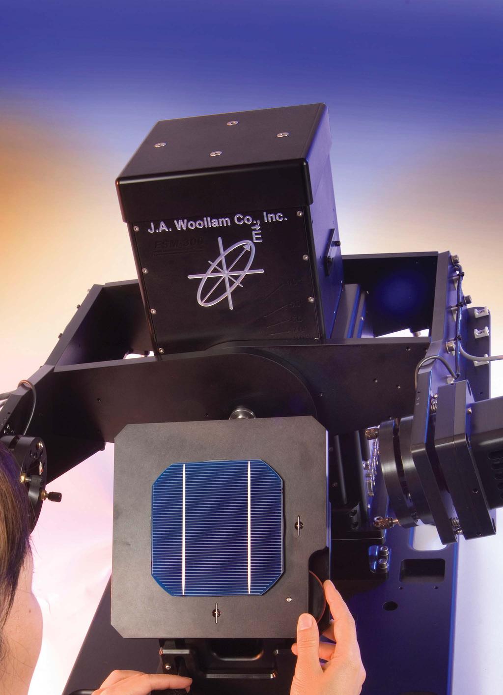
2 T-Solar Overview The T-Solar system combines our best photovoltaic measurement technology into a system designed specifically for measuring textured samples. Based on the established M-2000 rotating compensator spectroscopic ellipsometer, the T-Solar simultaneously measures hundreds of wavelengths across the UV-Visible-NIR. To improve performance on rough, textured surfaces that significantly reduce reflected signal, the T-Solar combines a special High-Intensity Lamp source with our new Intensity-Optimizer*. The T-Solar is perfect for characterizing AR coatings on etched silicon surfaces. In addition, the T-Solar features an adjustable tilt-rotation-stage*, which is required to align the pyramid structures of alkaline-etched monocrystalline surfaces 1. * Patent-pending 1 J. Sun et al., Characterizing AntiReflection Coatings on textured Mono-Crystalline Silicon with Spectroscopic Ellipsometry, submitted to IEEE 34th PVSC Proc., 2009.
 Transparent Conductive Oxides ITO ZnO x doped SnO 2 AZO a-si, µc-si, poly-si CdTe, CdS, CIGS Organic")


3 PV Applications Textured Mono- and Multicrystalline Substrates AR Coatings (SiN x, AlN x...) Transparent Conductive Oxides ITO ZnO x doped SnO 2 AZO a-si, µc-si, poly-si CdTe, CdS, CIGS Organic PV Materials Dye Sensitized Films The Intensity-Optimizer* allows convenient control of measurement signal to match the ideal range for any sample. Very useful when switching between metal, glass, and even textured substrates that will have a large variation in refl ected signal. T-Solar Sample Stage is fully adjustable for textured, pyramidal surfaces. Tilt and rotate sample to align pyramid facets with ellipsometer probe-beam.


4 T-Solar Measurements The T-Solar system was specifically designed to measure thin film coatings on textured substrates, such as those shown below. Both the texturing and AR coating are designed to suppress reflection from the surface making optical characterization challenging. (a) (b) 20µm 50µm Examples of textured surfaces, coated with single-layer SiN x as AR coating. Alkaline-etched Monocrystalline Si The texturing produced from alkaline etching of monocrystalline silicon produces a regular pattern of pyramids etched along specified directions of the silicon crystal. To measure this regular pattern of pyramids requires the special T-Solar measurement geometry. With the T-Solar, the sample stage can be tilted (and rotated) from the Standard Geometry to align the pyramids with the probe beam used for measurement. *patent-pending.
")


 to the")


5 Standard Geometry Lateral (Tilt) Geometry Ψ in degrees Ψ at 80 at in degrees Wavelength (nm) The measurement confi guration can be moved from standard geometry (for lightly textured samples dominated by smooth, fl at regions) to the Lateral (Tilt) Geometry for samples dominated by textured pyramid surfaces. As shown in the fi gure, the data are very noisy due to lack of signal if the wrong geometry is measured. The T-Solar provides adjustable fl exibility to measure in any geometry needed for any degree of textured and non-textured surfaces.


6 Modeling Experimental data are shown from a monocrystalline silicon substrate measured on the Woollam T-Solar ellipsometer. Standard smooth surface model does not reproduce the effects from pyramid structure and needs to be supplemented by a scattering factor to correctly reproduce the Experimental Data.


7 T-Solar data from AR coating on textured monocrystalline silicon are also corrected to match the effects from rough, textured surface. Even with the optimized intensity, the low reflectivity from textured surfaces push measurements to very oblique angles. Measured data and corresponding model fi t for a single-layer AR coating on multicrystalline silicon. Resulting optical constants for the AR coating are also shown.
8 Specifications Ellipsometer Technology M-2000 with Rotating Compensator Technology Base Options Manual Angle or Automated Angle Angle Range: 45 to 90 Horizontal Sample for standard measurement. Special Tilt (0-60 ) and Continuous Sample Rotation for Mono-crystalline Textured Surfaces Wavelength Range 245nm to 1000nm, approximately 470 total wavelengths Detection System CCD detector for simultaneous collection of all wavelengths. Measurement Time All wavelengths collected in less than 1 second. Longer averaging (up to 20 seconds) may be necessary for the low-light conditions of textured solar cells. Intensity Optimizer Patented method to manually adjust the measurement beam intensity. Adjust to optimize for both rough and smooth surfaces. J.A. Woollam Co., Inc. 645 M Street, Suite 102 Lincoln, NE USA Ph Fx
Spectroscopic Ellipsometer --- J. A. Woollam alpha-se
 Spectroscopic Ellipsometer --- J. A. Woollam alpha-se Introduction Figure 1: J. A. Woollam alpha-se spectroscopic ellipsometer An ellipsometer measures the change in polarization as light reflects or transmits
Laser Applications for Photovoltaics Crystalline and Thin Film Technologies
 LASERS & MATERIAL PROCESSING I OPTICAL SYSTEMS I INDUSTRIAL METROLOGY I TRAFFIC SOLUTIONS I DEFENSE & CIVIL SYSTEMS Laser Applications for Photovoltaics Crystalline and Thin Film Technologies Back contact
Laser Applications for Photovoltaics Crystalline and Thin Film Technologies
 LASERS & MATERIAL PROCESSING I OPTICAL SYSTEMS I INDUSTRIAL METROLOGY I TRAFFIC SOLUTIONS I DEFENSE & CIVIL SYSTEMS Laser Applications for Photovoltaics Crystalline and Thin Film Technologies Back contact
Woollam M2000 Operation Manual
 Woollam M2000 Operation Manual The Woollam M2000 is a spectroscopic ellipsometer used to characterize optically transparent films. The system has the Near IR upgrade that covers 700 wavelengths from 193nm
Specification of Thin Film Thickness Measuring Equipment
 of Thin Film Thickness Measuring Equipment A. Application: Major application is for solar cell thin film thickness measurement for films such as CIGS, CdS, ITO, ZnO etc. deposited on substrates such as
Session 1B Transparent Materials
 Session 1B Transparent Materials Andrew Martin UPenn, February 2014 2014 J.A. Woollam Co., Inc. www.jawoollam.com 1 Overview Transparent substrates & films Cauchy equation Common complexities Evaluating,
Reflectivity Calculation Program
 Reflectivity Calculation Program This optional program allows calculation of the reflectivity spectrum at any incidence angle from the wavelength distribution of the sample n and k values. Additionally,
5.2.2 Pins on the alignment detector are fragile. Use caution when inserting and removing the detector. Report any broken pins to staff.
 Title: Woollam Vase Approved by: Process Engineer / / / / Equipment Engineer 1 SCOPE The purpose of this document is to detail the use of the Woollam VASE. All users are expected to have read and understood
Standard Operating Manual
 Standard Operating Manual J.A. Woolam M-2000V Spectroscopic Ellipsometer Version 1.0 Page 1 of 13 Contents 1. Picture and Location 2. Process Capabilities 2.1 Cleanliness Standard 2.2 Features 2.3 Sample
Optical Topography Measurement of Patterned Wafers
 Optical Topography Measurement of Patterned Wafers Xavier Colonna de Lega and Peter de Groot Zygo Corporation, Laurel Brook Road, Middlefield CT 6455, USA xcolonna@zygo.com Abstract. We model the measurement
NRF Ellipsometer SOP Revision /19/15 Page 1 of 14. Ellipsometer SOP
 Page 1 of 14 Ellipsometer SOP The J. A. Woollam M88 is a spectroscopic ellipsometer used to measure film thickness and optical constants of transparent/semi-transparent thin films. It uses a Xenon arc
Light management in thin-film Si solar cells. Hitoshi Sai
 9th Aug. 2011 University of Southampton Light management in thin-film Si solar cells Hitoshi Sai Research Center for Photovoltaic Technology (RCPVT) National Institute of Advance Industrial Science & Technology
Operation Manual of J.A. Woollam Ellipsometer
 Operation Manual of J.A. Woollam Ellipsometer 1) Press both the Lamp power and lamp Ignition buttons to turn them on (The buttons are located on the front panel of the bottom control box). 2) Put your
A New Approach to Characterizing Surface Texturing of Crystalline Silicon Wafers for High Efficiency Solar Cells Application
 Technical Communication JLMN-Journal of Laser Micro/Nanoengineering Vol. 6, No. 3, 211 A New Approach to Characterizing Surface Texturing of Crystalline Silicon Wafers for High Efficiency Solar Cells Application
1A: Introduction to WVASE Data Analysis
 2014 J.A. Woollam Co., Inc. www.jawoollam.com 1 1A: Introduction to WVASE Data Analysis Nina Hong U Penn, February 2014 Session Outline 1. Introduction to Ellipsometry. 2. Classification of Samples. Transparent
Appendix A: Comparison of ray-tracing with Birandy and Sunrays programs
 Comparison of ray-tracing with Birandy and Sunrays programs Appendix A: Comparison of ray-tracing with Birandy and Sunrays programs Comparison of ray-tracing programs Birandy and Sunrays In order to check
Photo Emission Tech., Inc. 760 Calle Plano, Camarillo, CA USA Tel: (805) Fax: (805)
 Fax: (805)") IQE1800 SYSTEM INTRODUCTION Quantum Efficiency (QE) measurements provide a primary characterization method for completed photovoltaic devices. QE system provides electronics and software designed for fully
IQE1800 SYSTEM INTRODUCTION Quantum Efficiency (QE) measurements provide a primary characterization method for completed photovoltaic devices. QE system provides electronics and software designed for fully
Effect of Pre-Cleaning on Texturization of c-si Wafers in a KOH/IPA Mixture. Gim Chen and Ismail Kashkoush
 Effect of Pre-Cleaning on Texturization of c-si Wafers in a KOH/IPA Mixture Gim Chen and Ismail Kashkoush Akrion Systems LLC, 6330 Hedgewood Drive, #150, Allentown, PA 18106, USA Experiments were performed
Veeco Expands Solar Equipment Product Line Acquisition of Mill Lane Engineering. May 22, 2008
 Veeco Expands Solar Equipment Product Line Acquisition of Mill Lane Engineering May 22, 2008 Veeco Expands Thin Film Solar Equipment Product Line Completed purchase of Mill Lane Engineering Privately held
The NA PV Materials TC Chapter reviewed and recommended to issue for reapproval ballot.
 Background Statement for SEMI Draft Document 5905 REAPPROVAL OF SEMI PV15-0211 GUIDE FOR DEFINING CONDITIONS FOR ANGLE RESOLVED LIGHT SCATTER MEASUREMENTS TO MONITOR THE SURFACE ROUGHNESS AND TEXTURE OF
Effective Medium Theory, Rough Surfaces, and Moth s Eyes
 Effective Medium Theory, Rough Surfaces, and Moth s Eyes R. Steven Turley, David Allred, Anthony Willey, Joseph Muhlestein, and Zephne Larsen Brigham Young University, Provo, Utah Abstract Optics in the
ECE 595, Section 10 Numerical Simulations Lecture 33: Introduction to Finite- Difference Time-Domain Simulations. Prof. Peter Bermel April 3, 2013
 ECE 595, Section 10 Numerical Simulations Lecture 33: Introduction to Finite- Difference Time-Domain Simulations Prof. Peter Bermel April 3, 2013 Recap from Monday Numerical ODE solvers Initial value problems
NEW OPTICAL MEASUREMENT TECHNIQUE FOR SI WAFER SURFACE DEFECTS USING ANNULAR ILLUMINATION WITH CROSSED NICOLS
 NEW OPTICAL MEASUREMENT TECHNIQUE FOR SI WAFER SURFACE DEFECTS USING ANNULAR ILLUMINATION WITH CROSSED NICOLS Satoru Takahashi 1, Takashi Miyoshi 1, Yasuhiro Takaya 1, and Takahiro Abe 2 1 Department of
2.2. Facilities Requirements
 2.2. Facilities Requirements Facilities requirements for the alpha-se system are listed in Table 2-1 and the system dimensions are given in Figure 2-1. As shown in Figure 2-2, the preferred clear work
IRRADIANCE DISTRIBUTION OF IMAGE SURFACE IN MICROLENS ARRAY SOLAR CONCENTRATOR
 IRRADIANCE DISTRIBUTION OF IMAGE SURFACE IN MICROLENS ARRAY SOLAR CONCENTRATOR Ali H. Al-Hamdani 1, Hayfa G. Rashid 2 and Alaa B. Hasan 3 1 Department of Laser and Optoelectronics Engineering, University
Investigation of the foot-exposure impact in hyper-na immersion lithography when using thin anti-reflective coating
 Investigation of the foot-exposure impact in hyper-na immersion lithography when using thin anti-reflective coating Darron Jurajda b, Enrico Tenaglia a, Jonathan Jeauneau b, Danilo De Simone a, Zhimin
Reproducing the hierarchy of disorder for Morpho-inspired, broad-angle color reflection
 Supplementary Information for Reproducing the hierarchy of disorder for Morpho-inspired, broad-angle color reflection Bokwang Song 1, Villads Egede Johansen 2,3, Ole Sigmund 3 and Jung H. Shin 4,1,* 1
Thin silicon solar cells with SiО х /SiN x Bragg mirror rear surface reflector
 PACS 42.79.Bh, 78.66.Db, 84.6.Jt Thin silicon solar cells with О х / x Bragg mirror rear surface reflector I.I. Ivanov 1, T.V. ychyporuk 2, V.A. Skryshevsky 1, M. Lemiti 2 1 Taras Shevchenko Kyiv ational
Modeling of Surface Reflectance of Acid Textured Multicrystalline Silicon Wafer for Solar Cell Application
 International Journal of Electronics and Computer Science Engineering 1065 Available Online at www.ijecse.org ISSN- 2277-1956 Modeling of Surface Reflectance of Acid Textured Multicrystalline Silicon Wafer
1 Introduction j3. Thicknesses d j. Layers. Refractive Indices. Layer Stack. Substrates. Propagation Wave Model. r-t-φ-model
 j1 1 Introduction Thin films of transparent or semitransparent materials play an important role in our life. A variety of colors in nature are caused by the interference of light reflected at thin transparent
SemiconSoft, Inc. Optical Metrology Company. MProbe: Measurement Guide Thin-films measurement using Reflectance or/and Transmittance spectroscopy
 MProbe: Measurement Guide Thin-films measurement using Reflectance or/and Transmittance spectroscopy It is easy to be a measurement expert with MProbe The Purpose This document describes the measurement
SOLAR CELL SURFACE INSPECTION USING 3D PROFILOMETRY
 SOLAR CELL SURFACE INSPECTION USING 3D PROFILOMETRY Prepared by Benjamin Mell 6 Morgan, Ste16, Irvine CA 92618 P: 949.461.9292 F: 949.461.9232 nanovea.com Today's standard for tomorrow's materials. 21
ANOMALOUS SCATTERING FROM SINGLE CRYSTAL SUBSTRATE
 177 ANOMALOUS SCATTERING FROM SINGLE CRYSTAL SUBSTRATE L. K. Bekessy, N. A. Raftery, and S. Russell Faculty of Science, Queensland University of Technology, GPO Box 2434, Brisbane, Queensland, Australia
Thin film solar cell simulations with FDTD
 Thin film solar cell simulations with FDTD Matthew Mishrikey, Prof. Ch. Hafner (IFH) Dr. P. Losio (Oerlikon Solar) 5 th Workshop on Numerical Methods for Optical Nano Structures July 7 th, 2009 Problem
Theoretical Investigation of Light Trapping in Polycrystalline Silicon Thin-Film Solar Cells
 Available online at www.sciencedirect.com Energy Procedia 25 (2012 ) 43 49 PV Asia Pacific Conference 2011 Theoretical Investigation of Light Trapping in Polycrystalline Silicon Thin-Film Solar Cells Cangming
Texturing industrial multicrystalline silicon solar cells
 Solar Energy 76 (2004) 277 283 www.elsevier.com/locate/solener Texturing industrial multicrystalline silicon solar cells D.H. Macdonald a, *, A. Cuevas a, M.J. Kerr a, C. Samundsett a, D. Ruby b, S. Winderbaum
Mu lt i s p e c t r a l
 Viewing Angle Analyser Revolutionary system for full spectral and polarization measurement in the entire viewing angle EZContrastMS80 & EZContrastMS88 ADVANCED LIGHT ANALYSIS by Field iris Fourier plane
Holographic Elements in Solar Concentrator and Collection Systems
 Holographic Elements in Solar Concentrator and Collection Systems Raymond K. Kostuk,2, Jose Castro, Brian Myer 2, Deming Zhang and Glenn Rosenberg 3 Electrical and Computer Engineering, Department University
Microstructured anti-reflection surface design for the omni-directional solar cells
 Microstructured anti-reflection surface design for the omni-directional solar cells Li Chen, Hongjun Yang, Men Tao and Weidong Zhou Department of Electrical Engineering, NanoFAB Center, University of Texas
Wavelength scanning interferometry for measuring transparent films of the fusion targets
 Wavelength scanning interferometry for measuring transparent films of the fusion targets F. Gao *, X. Jiang, H. Muhamedsalih and H. Martin Centre for precision Technologies, University of Huddersfield,
Discover 3D measurements for flexible electronics: a metrology masterclass
 Discover 3D measurements for flexible electronics: a metrology masterclass Samuel Lesko Bruker Nano Surfaces 21 November 2013 Smithers Pira the worldwide authority on the packaging, paper and print industry
PERFORMANCE OF SILICON SOLAR CELL WITH VARIOUS SURFACE TEXTURES
 J.Ilm.Tek.Energi Vol.1 No.7 August 2008: 16-23 PERFORMANCE OF SILICON SOLAR CELL WITH VARIOUS SURFACE TEXTURES F. Jahanshah*, K. Sopian*, I. Ahmad*, M. Y. Othman*, S. H. Zaidi** * Solar Energy Research
10.5 Polarization of Light
 10.5 Polarization of Light Electromagnetic waves have electric and magnetic fields that are perpendicular to each other and to the direction of propagation. These fields can take many different directions
Three-Dimensional Point-Focus Spectral Splitting Solar Concentrator System
 International Journal of Optics and Applications 2014, 4(4A): 6-11 DOI: 10.5923/s.optics.201401.02 Three-Dimensional Point-Focus Spectral Splitting Solar Concentrator System Carlo Maragliano 1,*, Ahmed
Understanding and selecting diffraction gratings
 Understanding and selecting diffraction gratings Diffraction gratings are used in a variety of applications where light needs to be spectrally split, including engineering, communications, chemistry, physics
From Color to Chemometrics
 From Color to Chemometrics Strategies to determine coating thickness and quality Preliminary Version AIMCAL Web Coating & Handling Conference 2016 02.06.2016 Chris Hellwig Agenda 1 About us 2 Process and
Advanced light management techniques for building integrated PV (BIPV)
") Advanced light management techniques for building integrated PV (BIPV) A. Ingenito, J. C. O. Lizcano, O. Isabella, M. Zeman Delft University of Technology Advanced light management Roadmap for decreasing
Advanced light management techniques for building integrated PV (BIPV) A. Ingenito, J. C. O. Lizcano, O. Isabella, M. Zeman Delft University of Technology Advanced light management Roadmap for decreasing
Broadband and Wide Angle Antireflection Coatings for Solar Cell Applications Dr. Mohammed A. Hussein, Dr. Ali H. Al-Hamdani, Nibras S.
 Broadband and Wide Angle Antireflection Coatings for Solar Cell Applications Dr. Mohammed A. Hussein University of Technology Dr. Ali H. Al-Hamdani Energy and Renewable Energy Technology Center/ University
Chapter 1 Introduction
 Chapter 1 Introduction 1.1 MOTIVATION 1.1.1 LCD Industry and LTPS Technology [1], [2] The liquid-crystal display (LCD) industry has shown rapid growth in five market areas, namely, notebook computers,
Alkaline Etching for Reflectance Reduction in Multicrystalline Silicon Solar Cells
 G408 Journal of The Electrochemical Society, 151 6 G408-G427 2004 0013-4651/2004/151 6 /G408/20/$7.00 The Electrochemical Society, Inc. Alkaline Etching for Reflectance Reduction in Multicrystalline Silicon
Standard Operating Procedure FS-1 Film Sense Ellipsometer (spectroscopic)
") Standard Operating Procedure FS-1 Film Sense Ellipsometer (spectroscopic) The Film Sense FS-1 is a spectroscopic ellipsometer dedicated to advanced and rapid characterization of thin film structures for
Standard Operating Procedure FS-1 Film Sense Ellipsometer (spectroscopic) The Film Sense FS-1 is a spectroscopic ellipsometer dedicated to advanced and rapid characterization of thin film structures for
Microstructured surface design for omnidirectional antireflection coatings on solar cells
 JOURNAL OF APPLIED PHYSICS 102, 103105 2007 Microstructured surface design for omnidirectional antireflection coatings on solar cells Weidong Zhou, a Meng Tao, b Li Chen, and Hongjun Yang Department of
Step Height Comparison by Non Contact Optical Profiler, AFM and Stylus Methods
 AdMet 2012 Paper No. NM 002 Step Height Comparison by Non Contact Optical Profiler, AFM and Stylus Methods Shweta Dua, Rina Sharma, Deepak Sharma and VN Ojha National Physical Laboratory Council of Scientifi
Properties of Light. 1. The Speed of Light 2. The Propagation of Light 3. Reflection and Refraction 4. Polarization
 Chapter 33 - Light Properties of Light 1. The Speed of Light 2. The Propagation of Light 3. Reflection and Refraction 4. Polarization MFMcGraw-PHY 2426 Chap33-Light - Revised: 6-24-2012 2 Electromagnetic
2.626 Fundamentals of Photovoltaics
 MIT OpenCourseWare http://ocw.mit.edu 2.626 Fundamentals of Photovoltaics Fall 2008 For information about citing these materials or our Terms of Use, visit: http://ocw.mit.edu/terms. Efficiency Limits
ACCURATE TEXTURE MEASUREMENTS ON THIN FILMS USING A POWDER X-RAY DIFFRACTOMETER
 ACCURATE TEXTURE MEASUREMENTS ON THIN FILMS USING A POWDER X-RAY DIFFRACTOMETER MARK D. VAUDIN NIST, Gaithersburg, MD, USA. Abstract A fast and accurate method that uses a conventional powder x-ray diffractometer
4D Technology Corporation
 4D Technology Corporation Dynamic Laser Interferometry for Company Profile Disk Shape Characterization DiskCon Asia-Pacific 2006 Chip Ragan chip.ragan@4dtechnology.com www.4dtechnology.com Interferometry
2.) An overhead projector forms an image of a transparency on a screen:
 An overhead projector forms an image of a transparency on a screen:") 1.) You have measured the wavelength λ of a spectral lamp using a diffraction grating and the relation λ = d sin Θ. Your uncertainty in the grating spacing d is 0.5% and your uncertainty in your angle
1.) You have measured the wavelength λ of a spectral lamp using a diffraction grating and the relation λ = d sin Θ. Your uncertainty in the grating spacing d is 0.5% and your uncertainty in your angle
AltaSens A5262-4T 4.5 Megapixel CMOS Image Sensor 0.18 µm IBM Process
 AltaSens A5262-4T 4.5 Megapixel CMOS Image Sensor 0.18 µm IBM Process Imager Process Review For comments, questions, or more information about this report, or for any additional technical needs concerning
Spectrophotometric Methods of Refractive Indices Measurement
 Application Note Glass, ceramics, optics Spectrophotometric Methods of Refractive Indices Measurement Measuring the refractive index of single crystal optical materials using two methods Authors N.S. Kozlova
SE800 Short Manual SENTECH Instruments GmbH
 SE800 Spectroscopic Ellipsometry Documentation SE800 Page 2 of 16 Documentation SE800 SE 800 Page 3 of 16 Documentation SE800 Document Information: Authors: Date: File: Version: 2/5/2004 3:24:34 PM SE800_ShortManual.doc
Characterization of stratified media using high-resolution thin film measurement techniques
 Characterization of stratified media using high-resolution thin film measurement techniques Alberto Aguerri Sensofar-Tech, S.L. Crt. N150 Km14.5 IPCT Mòdul TR-20, 08227 Terrassa (Barcelona), Spain E-mail:
Agilent Cary Universal Measurement Spectrophotometer (UMS)
") Agilent Cary Universal Measurement Spectrophotometer (UMS) See what you ve been missing Date: 13 th May 2013 TRAVIS BURT UV-VIS-NIR PRODUCT MANAGER AGILENT TECHNOLOGIES 1 Agenda Introducing the Cary 7000
Agilent Cary Universal Measurement Spectrophotometer (UMS) See what you ve been missing Date: 13 th May 2013 TRAVIS BURT UV-VIS-NIR PRODUCT MANAGER AGILENT TECHNOLOGIES 1 Agenda Introducing the Cary 7000
3. Using TFCompanion. 3.1 Filmstack. Introduction Layer types and properties
 3. Using TFCompanion. 3.1 Filmstack. Introduction. Filmstack is an optical model of the sample that is measured - it consists of a substrate, collection of layers and an ambient. There is no limitation
Available online at ScienceDirect. Energy Procedia 92 (2016 )
") Available online at www.sciencedirect.com ScienceDirect Energy Procedia 92 (2016 ) 505 514 6th International Conference on Silicon Photovoltaics, SiliconPV 2016 Increased light harvesting by structured
Available online at www.sciencedirect.com ScienceDirect Energy Procedia 92 (2016 ) 505 514 6th International Conference on Silicon Photovoltaics, SiliconPV 2016 Increased light harvesting by structured
CompleteEASE Data Analysis Manual
 Version 3.65 CompleteEASE Data Analysis Manual By J. A. Woollam Co., Inc. June 15, 2008 Copyright 2004-2008 J. A. Woollam Co., Inc. All Rights Reserved. J. A. Woollam Co., Inc. 645 M Street, Suite 102
Chapter 2: Wave Optics
 Chapter : Wave Optics P-1. We can write a plane wave with the z axis taken in the direction of the wave vector k as u(,) r t Acos tkzarg( A) As c /, T 1/ and k / we can rewrite the plane wave as t z u(,)
3D Surface Metrology on PV Solar Wafers
 3D Surface Metrology on PV Solar Wafers Karl- Heinz Strass cybertechnologies USA 962 Terra Bella Ave San Jose CA 95125 P: 408-689-8144 www.cybertechnologies.com Introduction Solar photovoltaics is the
Manual for solar cell optical simulation software: GENPRO4
 Manual for solar cell optical simulation software: GENPRO4 Rudi Santbergen (r.santbergen@tudelft.nl) Photovoltaic Materials and Devices Delft University of Technology Version: February 2016 0. Introduction
OPTOELECTRONIC DESIGN OF MULTIJUNCTION WIRE-ARRAY SOLAR CELLS
 OPTOELECTRONIC DESIGN OF MULTIJUNCTION WIRE-ARRAY SOLAR CELLS Daniel B. Turner-Evans 1, Michael D. Kelzenberg 1, Chris T. Chen 1, Emily C. Warmann 1, Adele C. Tamboli 1, and Harry A. Atwater 1,2 1 Thomas
University of Minnesota Nano Fabrication Center Standard Operating Procedure
 Equipment Name: Film-Sense Coral Name: film-sense Revision Number: 1 Model: FS-1 Revisionist: T. Whipple Location: Bay 1 Date: 5/16/2017 1 Description The Film Sense FS-1 Multi-Wavelength Ellipsometer
ksa ICE - Integrated Control for Epitaxy
 Introduction The k-space Integrated Control for Epitaxy system (ksa ICE) is a modular in-situ metrology tool designed for today s MOCVD reactors. It combines proven ksa MOS, ksa BandiT, and ksa RateRat
WORCESTER POLYTECHNIC INSTITUTE
 WORCESTER POLYTECHNIC INSTITUTE MECHANICAL ENGINEERING DEPARTMENT Optical Metrology and NDT ME-593L, C 2018 Introduction: Wave Optics January 2018 Wave optics: coherence Temporal coherence Review interference
The Advantages of Dye-Doped Liquid Crystals in Constructing a Fresnel Zone Plate Lens
 The Advantages of Dye-Doped Liquid Crystals in Constructing a Fresnel Zone Plate Lens Joshua T. Wiersma (jwiersma@email.arizona.edu) College of Optical Sciences, University of Arizona, Tucson, Arizona
SILICON PHOTONICS WAVEGUIDE AND ITS FIBER INTERCONNECT TECHNOLOGY. Jeong Hwan Song
 SILICON PHOTONICS WAVEGUIDE AND ITS FIBER INTERCONNECT TECHNOLOGY Jeong Hwan Song CONTENTS Introduction of light waveguides Principals Types / materials Si photonics Interface design between optical fiber
Sony ICX098BL ¼ Inch Optical Format 5.6 µm Pixel Size CCD Image Sensor
 Sony ICX098BL ¼ Inch Optical Format 5.6 µm Pixel Size CCD Image Sensor Custom Imager Process Review For comments, questions, or more information about this report, or for any additional technical needs
Length Scale Dependence of Periodic Textures for Photoabsorption Enhancement in Ultra-thin Silicon Foils and Thick Wafers
 Length Scale Dependence of Periodic Textures for Photoabsorption Enhancement in Ultra-thin Silicon Foils and Thick Wafers K Kumar 1, A Khalatpour 2, G Liu 1, J Nogami 1* and N P Kherani 1, 2 1 Department
Manufacturing Challenges for Lithography in the Textured Disc Paradigm. September 18 th, 2008 Babak Heidari
 Manufacturing Challenges for Lithography in the Textured Disc Paradigm September 18 th, 2008 Babak Heidari Longitudinal Perpendicular Pattern media + HAMR 6,25 T/in 2 TDK: DTR 602 Gb/in 2 1 T/in 2 150
Lecture 4: Reflection Models
 Lecture 4: Reflection Models CS 660, Spring 009 Kavita Bala Computer Science Cornell University Outline Light sources Light source characteristics Types of sources Light reflection Physics-based models
HYPERSPECTRAL IMAGING THIN FILM APPLICATIONS. Dr. Wulf Grählert /
 Dr. Wulf Grählert +49 351 / 83391 3406 wulf.graehlert@iws.fraunhofer.de Motivation Coating processes: thin film application process stability What s about Monitoring? Random sampling? Real time analysis?
Lab 12 - Interference-Diffraction of Light Waves
 Lab 12 - Interference-Diffraction of Light Waves Equipment and Safety: No special safety equipment is required for this lab. Do not look directly into the laser. Do not point the laser at other people.
Physics 309 Lab 3. where the small angle approximation has been used. This pattern has maxima at. Y Max. n L /d (2)
") Physics 309 Lab 3 Introduction This will be a lab whose purpose is to give you some hands-on experience with optical interference and diffraction, using small green diode lasers as the light sources. Each
Physics 309 Lab 3 Introduction This will be a lab whose purpose is to give you some hands-on experience with optical interference and diffraction, using small green diode lasers as the light sources. Each
Plano-Convex Lenses. Read further. Catalog Items BK7 Plano-Convex Lenses. Description. Standard specifications. Features.
 Plano-Convex Lenses (PCX) PCX positive focal length lenses have flat surface on one side and spherical surface on the other. They are used for focusing beams in telescopes, collimators or condenser systems,
Chapter 24. Wave Optics. Wave Optics. The wave nature of light is needed to explain various phenomena
 Chapter 24 Wave Optics Wave Optics The wave nature of light is needed to explain various phenomena Interference Diffraction Polarization The particle nature of light was the basis for ray (geometric) optics
Optical properties and characterization
 Optical properties and characterization Name Picture Description Site Responsible 1 Laser Nd:YAG MAPLE (Matrix Assisted Pulsed Laser Evaporation) system for biomaterials and polymeric thin film deposition
MEMS SENSOR FOR MEMS METROLOGY
 MEMS SENSOR FOR MEMS METROLOGY IAB Presentation Byungki Kim, H Ali Razavi, F. Levent Degertekin, Thomas R. Kurfess 9/24/24 OUTLINE INTRODUCTION Motivation Contact/Noncontact measurement Optical interferometer
IB-2 Polarization Practice
 Name: 1. Plane-polarized light is incident normally on a polarizer which is able to rotate in the plane perpendicular to the light as shown below. In diagram 1, the intensity of the incident light is 8
Measurement and Standards: The Role of NIST
 Measurement and Standards: The Role of NIST Dr. Kent Rochford, Acting Director Electrical and Electronics Engineering Laboratory (EEEL) National Institute of Standards and Technology Department of Commerce
Reflectivity metrics for optimization of anti-reflection coatings on wafers with topography
 Reflectivity metrics for optimization of anti-reflection coatings on wafers with topography Mark D. Smith, Trey Graves, John Biafore, and Stewart Robertson KLA-Tencor Corp, 8834 N. Capital of Texas Hwy,
OPSE FINAL EXAM Fall CLOSED BOOK. Two pages (front/back of both pages) of equations are allowed.
 of equations are allowed.") CLOSED BOOK. Two pages (front/back of both pages) of equations are allowed. YOU MUST SHOW YOUR WORK. ANSWERS THAT ARE NOT JUSTIFIED WILL BE GIVEN ZERO CREDIT. ALL NUMERICAL ANSERS MUST HAVE UNITS INDICATED.
CLOSED BOOK. Two pages (front/back of both pages) of equations are allowed. YOU MUST SHOW YOUR WORK. ANSWERS THAT ARE NOT JUSTIFIED WILL BE GIVEN ZERO CREDIT. ALL NUMERICAL ANSERS MUST HAVE UNITS INDICATED.
Introduction to XRD analysis of modern functional thin films using a 2-dimensional detector (1) GI-XRD
 GI-XRD") Technical articles Introduction to XRD analysis of modern functional thin films using a 2-dimensional detector (1) GI-XRD Shintaro Kobayashi* and Katsuhiko Inaba** 1. Introduction The development of new
Technical articles Introduction to XRD analysis of modern functional thin films using a 2-dimensional detector (1) GI-XRD Shintaro Kobayashi* and Katsuhiko Inaba** 1. Introduction The development of new
FILMETRICS F20 STANDARD OPERATION PROCEDURE
 Arizona State University NanoFab FILMETRICS F20 STANDARD OPERATION PROCEDURE Rev C Table of Contents Contents Table of Contents...1 1. Purpose / Scope...2 2. Reference Documents...2 3. Equipment / Supplies
SURFACE TEXTURE EFFECT ON LUSTER OF ANODIZED ALUMINUM USING 3D PROFILOMETRY
 SURFACE TEXTURE EFFECT ON LUSTER OF ANODIZED ALUMINUM USING 3D PROFILOMETRY Prepared by Duanjie Li, PhD 6 Morgan, Ste156, Irvine CA 92618 P: 949.461.9292 F: 949.461.9232 nanovea.com Today's standard for
AN INTRODUCTION TO THE SURFOPTIC IMAGING REFLECTOMETER
 AN INTRODUCTION TO THE SURFOPTIC IMAGING REFLECTOMETER N J Elton 1. INTRODUCTION The Surfoptic Imaging Reflectometer is a new generation of instrument for polarised light reflectometry of industrial materials.
Michelson Interferometer
 Michelson Interferometer The Michelson interferometer uses the interference of two reflected waves The third, beamsplitting, mirror is partially reflecting ( half silvered, except it s a thin Aluminum
MACHINING SURFACE FINISH QUALITY USING 3D PROFILOMETRY
 MACHINING SURFACE FINISH QUALITY USING 3D PROFILOMETRY Prepared by Duanjie Li, PhD Morgan, Ste1, Irvine CA 91 P: 99.1.99 F: 99.1.93 nanovea.com Today's standard for tomorrow's materials. 1 NANOVEA INTRODUCTION
AUTOFOCUS SENSORS & MICROSCOPY AUTOMATION IR LASER SCANNING CONFOCAL MICROSCOPE IRLC DEEP SEE. Now See Deeper than ever before
 AUTOFOCUS SENSORS & MICROSCOPY AUTOMATION IR LASER SCANNING CONFOCAL MICROSCOPE IRLC DEEP SEE Now See Deeper than ever before Review and inspection of non visible subsurface defects Non visible and subsurface
Chapter 24. Wave Optics
 Chapter 24 Wave Optics Wave Optics The wave nature of light is needed to explain various phenomena Interference Diffraction Polarization The particle nature of light was the basis for ray (geometric) optics
Chapter 24. Wave Optics. Wave Optics. The wave nature of light is needed to explain various phenomena
 Chapter 24 Wave Optics Wave Optics The wave nature of light is needed to explain various phenomena Interference Diffraction Polarization The particle nature of light was the basis for ray (geometric) optics
ScienceDirect. The multi-busbar design: an overview
 Erschienen in: Energy Procedia ; 43 (2013). - S. 86-92 Available online at www.sciencedirect.com ScienceDirect Energy Procedia 43 (2013 ) 86 92 4 th Workshop on Metallization for Crystalline Silicon Solar