8085 Microprocessor Programs
|
|
|
- Jesse Cox
- 6 years ago
- Views:
Transcription
1 8085 Microprocessor Programs Courtesy : Rachit Agrawal 07-CE-52 Kalol Institute of Technology & Research Center
2 PROGRAMS FOR 8085 MICROPROCESSOR PROGRAMS FOR LEARNERS 1. Store 8-bit data in memory 2. Exchange the contents of memory locations 3. Add two 8-bit numbers 4. Subtract two 8-bit numbers 5. Add two 16-bit numbers 6. Add contents of two memory locations 7. Subtract two 16-bit numbers. 8. Finding one's complement of a number 9. Finding Two's complement of a number 10. Pack the unpacked BCD numbers 11. Unpack a BCD number 12. Execution format of instructions 13. Right shift bit of data 14. Left Shifting of a 16-bit data 15. Alter the contents of flag register in 8085 PROGRAMS FOR BEGINNERS 16. Calculate the sum of series of numbers 17. Multiply two 8-bit numbers 18. Divide a 16 bit number by a 8-bit number 19. Find the negative numbers in a block of data. 20. Find the largest of given numbers 21. Count number of one's in a number 22. Arrange in ascending order 23. Calculate the sum of series of even numbers 24. Calculate the sum of series of odd numbers 25. Find the square of given number 26. Search a byte in a given number 27. Add two decimal numbers of 6 digit each 28. Add each element of array with the elements of another array 29. Separate even numbers from given numbers 30. Transfer contents to overlapping memory blocks PROGRAMS FOR TRAINEES 31. Add parity bit to 7-bit ASCII characters 32. Find the number of negative, zero and positive numbers 33. Inserting string in a given array of characters 34. Deleting string in a given array of characters 35. Multiply two eight bit numbers with shift and add method 36. Divide 16-bit number with 8-bit number using shifting technique 37. Sub routine to perform the task of DAA 38. Program to test RAM 39. Program to generate fibonacci number 40. Generate a delay of 0.4 seconds 41. Arrange in DESCENDING Order 42. Data transfer from one memory block to other memory block. 43. Find the factorial of a number 44. Find the Square Root of a given number 45. Split a HEX data into two nibbles and store it
3 46. Add two 4-digit BCD numbers 47. Subtraction of two BCD numbers 48. Multiply two 2-digit BCD numbers PROGRAMS FOR EXPERTS a.programs TO WORK WITH COUNTERS 49. Generate and display binary up counter 50. Generate and display BCD up counter with frequency 1Hz 51. Generate and display BCD down counter 52. Generate and display the contents of decimal counter 53. Debug the delay routine b.programs IN CODE CONVERSION Digit BCD to binary conversion. 55. Binary to BCD conversion 56. Find the 7-segment codes for given numbers 57. Find the ASCII character 58. ASCII to Decimal Conversion 59. HEX to Decimal conversion 60. HEX to binary conversion c.programs IN INTERFACING & APPLICTIONS I. Interfacing with IC 8251(Serial Communcation/USART) 61. Output byte from SOD pin 62. Generate square wave from SOD pin 63. Receive ASCII character through SID pin 64. Transmit message using Receive message using 8251 II. Interfacing with IC 8255( Programmable Periperal Interface - PPI) 66. Initialize Blink port C bit 0 of Flashing of LEDs 69. Traffic Light Control 70. Stepper Motor Control 71. Keyboard interface(64-key-matrix-keyboard) 72. Seven Segment Display Interface (Eight Digits) III. Interfacing with IC 8279 (Keyboard and Display Controller) x 8 Keyboard Interface(Without Interrupt signal) x 8 Keyboard Interface(With Interrupt signal) x 4 Matrix Keyboard Interface 76. Interfacing of eight 7-segment digits 77. Interfacing of 4x4 matrix keyboard and 4 digit 7 segment display 78. Roll a message - 'HELL0123' 79. Roll your NAME
4 1 Statement: Store the data byte 32H into memory location 4000H. Program 1: MVI A, 52H STA 4000H : Store 32H in the accumulator : Copy accumulator contents at address 4000H : Terminate program execution Program 2: LXI H MVI M (4000H) : Load HL with 4000H : Store 32H in memory location pointed by HL register pair : Terminate program execution The result of both programs will be the same. In program 1 direct addressing instruction is used, whereas in program 2 indirect addressing instruction is used. 2 Statement: Exchange the contents of memory locations 2000H and 4000H Program 1: LDA 2000H MOV B, A LDA 4000H STA 2000H MOV A, B STA 4000H Program 2: LXI H 2000H location 2000H. LXI D 4000H location 4000H. MOV B, M register. LDAX D MOV M, A 2000H. MOV A, B STAX D 4000H. : Get the contents of memory location 2000H into accumulator : Save the contents into B register : Get the contents of memory location 4000Hinto accumulator : Store the contents of accumulator at address 2000H : Get the saved contents back into A register : Store the contents of accumulator at address 4000H : Initialize HL register pair as a pointer to memory : Initialize DE register pair as a pointer to memory : Get the contents of memory location 2000H into B : Get the contents of memory location 4000H into A register. : Store the contents of A register into memory location : Copy the contents of B register into accumulator. : Store the contents of A register into memory location : Terminate program execution. In Program 1, direct addressing instructions are used, whereas in Program 2, indirect addressing instructions are used.
 = 14H (4001H) = 89H Result = 14H + 89H = 9DH Source program LXI H 4000H MOV A, M INX H ADD M INX H MOV M, A : HL points 4000H : Get first operand : HL points 4001H : Add second")
5 3 Statement: Add the contents of memory locations 4000H and 4001H and place the result in memory location 4002H. Sample problem (4000H) = 14H (4001H) = 89H Result = 14H + 89H = 9DH Source program LXI H 4000H MOV A, M INX H ADD M INX H MOV M, A : HL points 4000H : Get first operand : HL points 4001H : Add second operand : HL points 4002H : Store result at 4002H : Terminate program execution FLOWCHART
 (4001H) Result = 51H = 19H = 51H - 19H = 38H Source program: LXI H, 4000H : HL points 4000H MOV A, M : Get first operand INX H : HL")
6 4 Statement: Subtract the contents of memory location 4001H from the memory location 2000H and place the result in memory location 4002H. Program - 4: Subtract two 8-bit numbers Sample problem: (4000H) (4001H) Result = 51H = 19H = 51H - 19H = 38H Source program: LXI H, 4000H : HL points 4000H MOV A, M : Get first operand INX H : HL points 4001H SUB M : Subtract second operand INX H : HL points 4002H MOV M, A : Store result at 4002H. : Terminate program execution FLOWCHART
7 5 Statement: Add the 16-bit number in memory locations 4000H and 4001H to the 16-bit number in memory locations 4002H and 4003H. The most significant eight bits of the two numbers to be added are in memory locations 4001H and 4003H. Store the result in memory locations 4004H and 4005H with the most significant byte in memory location 4005H Program - 5.a: Add two 16-bit numbers - Source Program 1 Sample problem: (4000H) = 15H (4001H) = 1CH (4002H) = B7H (4003H) = 5AH Result = 1C15 + 5AB7H = 76CCH (4004H) = CCH (4005H) = 76H Source Program 1: LHLD 4000H : Get first I6-bit number in HL XCHG : Save first I6-bit number in DE LHLD 4002H : Get second I6-bit number in HL MOV A, E : Get lower byte of the first number ADD L : Add lower byte of the second number MOV L, A : Store result in L register MOV A, D : Get higher byte of the first number ADC H : Add higher byte of the second number with CARRY MOV H, A : Store result in H register SHLD 4004H : Store I6-bit result in memory locations 4004H and 4005H. : Terminate program execution Program - 5b: Add two 16-bit numbers - Source Program 2 Source program 2: LHLD 4000H : Get first I6-bit number XCHG : Save first I6-bit number in DE LHLD 4002H : Get second I6-bit number in HL DAD D : Add DE and HL SHLD 4004H : Store I6-bit result in memory locations 4004H and 4005H. : Terminate program execution NOTE: In program 1, eight bit addition instructions are used (ADD and ADC) and addition is performed in two steps. First lower byte addition using ADD instruction and then higher byte addition using ADC instruction.in program 2, 16-bit addition instruction (DAD) is used.
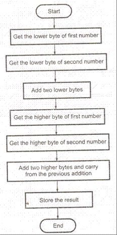
8 FLOWCHART
 = 7FH (400lH) = 89H Result = 7FH + 89H = lo8h (4002H) = 08H (4003H) = 0lH Source program: LXI H, 4000H MOV A, M INX H ADD M INX H MOV M, A MVIA, 00 ADC A INX H MOV M, A :HL")
9 6 Statement: Add the contents of memory locations 40001H and 4001H and place the result in the memory locations 4002Hand 4003H. Sample problem: (4000H) = 7FH (400lH) = 89H Result = 7FH + 89H = lo8h (4002H) = 08H (4003H) = 0lH Source program: LXI H, 4000H MOV A, M INX H ADD M INX H MOV M, A MVIA, 00 ADC A INX H MOV M, A :HL Points 4000H :Get first operand :HL Points 4001H :Add second operand :HL Points 4002H :Store the lower byte of result at 4002H :Initialize higher byte result with 00H :Add carry in the high byte result :HL Points 4003H :Store the higher byte of result at 4003H :Terminate program execution FLOWCHART
10 7 Statement: Subtract the 16-bit number in memory locations 4002H and 4003H from the 16-bit number in memory locations 4000H and 4001H. The most significant eight bits of the two numbers are in memory locations 4001H and 4003H. Store the result in memory locations 4004H and 4005H with the most significant byte in memory location 4005H. Sample problem (4000H) = 19H (400IH) = 6AH (4004H) = I5H (4003H) = 5CH Result = 6A19H - 5C15H = OE04H (4004H) = 04H (4005H) = OEH Source program: LHLD 4000H XCHG LHLD 4002H MOV A, E SUB L MOV L, A MOV A, D SBB H MOV H, A SHLD 4004H : Get first 16-bit number in HL : Save first 16-bit number in DE : Get second 16-bit number in HL : Get lower byte of the first number : Subtract lower byte of the second number : Store the result in L register : Get higher byte of the first number : Subtract higher byte of second number with borrow : Store l6-bit result in memory locations 4004H and 4005H. : Store l6-bit result in memory locations 4004H and 4005H. : Terminate program execution. FLOWCHART
 = 55H Result = (4300B) = AAB Source program: LDA 4400B CMA STA 4300H : Get the number : Complement number : Store the result : Terminate")
11 8 Statement: Find the l's complement of the number stored at memory location 4400H and store the complemented number at memory location 4300H. Sample problem: (4400H) = 55H Result = (4300B) = AAB Source program: LDA 4400B CMA STA 4300H : Get the number : Complement number : Store the result : Terminate program execution FLOWCHART
 = 55H Result = (4300H) = AAH + 1 = ABH Source program: LDA 4200H CMA ADI, 01 H STA 4300H : Get the number : Complement the number : Add one in the number : Store the")
12 9 Statement: Find the 2's complement of the number stored at memory location 4200H and store the complemented number at memory location 4300H. Sample problem: (4200H) = 55H Result = (4300H) = AAH + 1 = ABH Source program: LDA 4200H CMA ADI, 01 H STA 4300H : Get the number : Complement the number : Add one in the number : Store the result : Terminate program execution FLOWCHART
 = 04 (4201H) = 09 Result = (4300H) = 94 Source program LDA 4201H : Get the Most significant BCD digit RLC RLC RLC RLC : Adjust the position of the second digit (09 is changed")
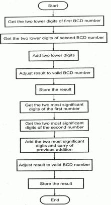
13 10 Statement: Pack the two unpacked BCD numbers stored in memory locations 4200H and 4201H and store result in memory location 4300H. Assume the least significant digit is stored at 4200H. Sample problem: (4200H) = 04 (4201H) = 09 Result = (4300H) = 94 Source program LDA 4201H : Get the Most significant BCD digit RLC RLC RLC RLC : Adjust the position of the second digit (09 is changed to 90) ANI FOH : Make least significant BCD digit zero MOV C, A : store the partial result LDA 4200H : Get the lower BCD digit ADD C : Add lower BCD digit STA 4300H : Store the result : Terminate program execution NOTE: BCD NO.: The numbers "0 to 9" are called BCD (Binary Coded Decimal) numbers. A decimal number 29 can be converted into BCD number by splitting FLOWCHART

14 11 Statement: Two digit BCD number is stored in memory location 4200H. Unpack the BCD number and store the two digits in memory locations 4300H and 4301H such that memory location 4300H will have lower BCD digit. Sample problem (4200H) = 58 Result = (4300H) = 08 and (4301H) = 05 Source program LDA 4200H ANI FOH RRC RRC RRC RRC STA 4301H LDA 4200H ANI OFH STA 4201H : Get the packed BCD number : Mask lower nibble : Adjust higher BCD digit as a lower digit : Store the partial result :.Get the original BCD number : Mask higher nibble : Store the result : Terminate program execution
15 12 Statement:Read the program given below and state the contents of all registers after the execution of each instruction in sequence. Main program: 4000H 4003H 4006H 4009H 400CH LXI SP, 27FFH LXI H, 2000H LXI B, 1020H CALL SUB Subroutine program: 4100H 4101H 4102H 4105H 4108H 4109H 410CH 410DH 410EH SUB: PUSH B PUSH H LXI B, 4080H LXI H, 4090H SHLD 2200H DAD B POP H POP B RET

16 13 Statement:Write a program to shift an eight bit data four bits right. Assume that data is in register C. Source program: MOV A, C RAR RAR RAR RAR MOV C, A Statement:Write a program to shift a 16 bit data, 1 bit right. Assume that data is in BC register pair. Source program: MOV A, B RAR MOV B, A MOV A, C RAR MOV C, A

17 14 Statement: Program to shift a 16-bit data 1 bit left. Assume data is in the HL register pair. Source program: DAD H : Adds HL data with HL data 15 Statement: Write a set of instructions to alter the contents of flag register in PUSH PSW POP H MOV A, L CMA MOV L, A PUSH H POP PSW : Save flags on stack : Retrieve flags in 'L' : Flags in accumulator : Complement accumulator : Accumulator in 'L' : Save on stack : Back to flag register :Terminate program execution 16 Statement: Calculate the sum of series of numbers. The length of the series is in memory location 4200H and the series begins from memory location 4201H. a. Consider the sum to be 8 bit number. So, ignore carries. Store the sum at memory location 4300H. b. Consider the sum to be 16 bit number. Store the sum at memory locations 4300H and 4301H. a. Sample problem 4200H = 04H 4201H = 10H 4202H = 45H 4203H = 33H 4204H = 22H Result = = H 4300H = H Source program: LDA 4200H MOV C, A : Initialize counter SUB A : sum = 0 LXI H, 420lH : Initialize pointer BACK: ADD M : SUM = SUM + data INX H : increment pointer DCR C : Decrement counter JNZ BACK : if counter 0 repeat STA 4300H : Store sum : Terminate program execution
18 FLOWCHART b. Sample problem 4200H = 04H 420lH = 9AH 4202H = 52H 4203H = 89H 4204H = 3EH Result = 9AH + 52H + 89H + 3EH = H 4300H = B3H Lower byte 4301H = 0lH Higher byte Source program: LDA 4200H MOV C, A : Initialize counter LXI H, 4201H : Initialize pointer SUB A :Sum low = 0 MOV B, A : Sum high = 0 BACK: ADD M : Sum = sum + data JNC SKIP INR B : Add carry to MSB of SUM SKIP: INX H : Increment pointer DCR C : Decrement counter JNZ BACK : Check if counter 0 repeat STA 4300H : Store lower byte MOV A, B STA 4301H : Store higher byte :Terminate program execution
19 17 Statement: Multiply two 8-bit numbers stored in memory locations 2200H and 2201H by repetitive addition and store the result in memory locations 2300H and 2301H. Sample problem: (2200H) = 03H (2201H) = B2H Result = B2H + B2H + B2H = 216H = 216H (2300H) = 16H (2301H) = 02H Source program LDA 2200H MOV E, A MVI D, 00 : Get the first number in DE register pair LDA 2201H MOV C, A : Initialize counter LX I H, 0000 H : Result = 0 BACK: DAD D : Result = result + first number DCR C : Decrement count JNZ BACK : If count 0 repeat SHLD 2300H : Store result : Terminate program execution FLOWCHART
20 18 Statement:Divide 16 bit number stored in memory locations 2200H and 2201H by the 8 bit number stored at memory location 2202H. Store the quotient in memory locations 2300H and 2301H and remainder in memory locations 2302H and 2303H. Sample problem (2200H) = 60H (2201H) = A0H (2202H) = l2h Result = A060H/12H = 8E8H Quotient and 10H remainder (2300H) = E8H (2301H) = 08H (2302H= 10H (2303H) 00H Source program LHLD 2200H : Get the dividend LDA 2202H : Get the divisor MOV C, A LXI D, 0000H : Quotient = 0 BACK: MOV A, L SUB C : Subtract divisor MOV L, A : Save partial result JNC SKIP : if CY 1 jump DCR H : Subtract borrow of previous subtraction SKIP: INX D : Increment quotient MOV A, H CPI, 00 : Check if dividend < divisor JNZ BACK : if no repeat MOV A, L CMP C JNC BACK SHLD 2302H : Store the remainder XCHG SHLD 2300H : Store the quotient : Terminate program execution
21 FLOWCHART
22 19 Statement:Find the number of negative elements (most significant bit 1) in a block of data. The length of the block is in memory location 2200H and the block itself begins in memory location 2201H. Store the number of negative elements in memory location 2300H Sample problem (2200H) = 04H (2201H) = 56H (2202H) = A9H (2203H) = 73H (2204H) = 82H Result = 02 since 2202H and 2204H contain numbers with a MSB of 1. Source program LDA 2200H MOV C, A : Initialize count MVI B, 00 : Negative number = 0 LXI H, 2201H : Initialize pointer BACK: MOV A, M : Get the number ANI 80H : Check for MSB JZ SKIP : If MSB = 1 INR B : Increment negative number count SKIP: INX H : Increment pointer DCR C : Decrement count JNZ BACK : If count 0 repeat MOV A, B STA 2300H : Store the result : Terminate program execution FLOWCHART
23 20 Statement:Find the largest number in a block of data. The length of the block is in memory location 2200H and the block itself starts from memory location 2201H. Store the maximum number in memory location 2300H. Assume that the numbers in the block are all 8 bit unsigned binary numbers. Sample problem (2200H) = 04 (2201H) = 34H (2202H) = A9H (2203H) = 78H (2204H) =56H Result = (2202H) = A9H Source program LDA 2200H MOV C, A : Initialize counter XRA A : Maximum = Minimum possible value = 0 LXI H, 2201H : Initialize pointer BACK: CMP M : Is number> maximum JNC SKIP : Yes, replace maximum MOV A, M SKIP: INX H DCR C JNZ BACK STA 2300H : Store maximum number : Terminate program execution FLOWCHART
24 21 Statement:Write a program to count number of l's in the contents of D register and store the count in the B register. Source program: MVI B, 00H MVI C, 08H MOV A, D BACK: RAR JNC SKIP INR B SKIP: DCR C JNZ BACK
25 22 Statement:Write a program to sort given 10 numbers from memory location 2200H in the ascending order. Source program: MVI B, 09 : Initialize counter START : LXI H, 2200H: Initialize memory pointer MVI C, 09H : Initialize counter 2 BACK: MOV A, M : Get the number INX H : Increment memory pointer CMP M : Compare number with next number JC SKIP : If less, don't interchange JZ SKIP : If equal, don't interchange MOV D, M MOV M, A DCX H MOV M, D INX H : Interchange two numbers SKIP:DCR C : Decrement counter 2 JNZ BACK : If not zero, repeat DCR B : Decrement counter 1 JNZ START : Terminate program execution
26 FLOWCHART
27 23 Statement:Calculate the sum of series of even numbers from the list of numbers. The length of the list is in memory location 2200H and the series itself begins from memory location 2201H. Assume the sum to be 8 bit number so you can ignore carries and store the sum at memory location 2210H. Sample problem: 2200H= 4H 2201H= 20H 2202H= l5h 2203H= l3h 2204H= 22H Result 22l0H= = 42H = 42H Source program: LDA 2200H MOV C, A : Initialize counter MVI B, 00H : sum = 0 LXI H, 2201H : Initialize pointer BACK: MOV A, M : Get the number ANI 0lH : Mask Bit l to Bit7 JNZ SKIP : Don't add if number is ODD MOV A, B : Get the sum ADD M : SUM = SUM + data MOV B, A : Store result in B register SKIP: INX H : increment pointer DCR C : Decrement counter JNZ BACK : if counter 0 repeat STA 2210H : store sum : Terminate program execution
28 FLOWCHART
29 24 Statement:Calculate the sum of series of odd numbers from the list of numbers. The length of the list is in memory location 2200H and the series itself begins from memory location 2201H. Assume the sum to be 16-bit. Store the sum at memory locations 2300H and 2301H. Sample problem: 2200H = 4H 2201H= 9AH 2202H= 52H 2203H= 89H 2204H= 3FH Result = 89H + 3FH = C8H 2300H= H Lower byte 2301H = H Higher byte Source program LDA 2200H MOV C, A : Initialize counter LXI H, 2201H : Initialize pointer MVI E, 00 : Sum low = 0 MOV D, E : Sum high = 0 BACK: MOV A, M : Get the number ANI 0lH : Mask Bit 1 to Bit7 JZ SKIP : Don't add if number is even MOV A, E : Get the lower byte of sum ADD M : Sum = sum + data MOV E, A : Store result in E register JNC SKIP INR D : Add carry to MSB of SUM SKIP: INX H : Increment pointer
30 FLOWCHART
31 25 Statement:Find the square of the given numbers from memory location 6100H and store the result from memory location 7000H. Source Program: LXI H, 6200H LXI D, 6100H LXI B, 7000H BACK: LDAX D MOV L, A MOV A, M STAX B INX D INX B MOV A, C CPI 05H JNZ BACK : Initialize lookup table pointer : Initialize source memory pointer : Initialize destination memory pointer : Get the number : A point to the square : Get the square : Store the result at destination memory location : Increment source memory pointer : Increment destination memory pointer : Check for last number : If not repeat : Terminate program execution
32 26 Statement: Search the given byte in the list of 50 numbers stored in the consecutive memory locations and store the address of memory location in the memory locations 2200H and 2201H. Assume byte is in the C register and starting address of the list is 2000H. If byte is not found store 00 at 2200H and 2201H. Source program: LX I H, 2000H MVI B, 52H BACK: MOV A, M CMP C JZ LAST INX H DCR B JNZ B LXI H, 0000H SHLD 2200H JMP END LAST: SHLD 2200H END: : Initialize memory pointer 52H : Initialize counter : Get the number : Compare with the given byte : Go last if match occurs : Increment memory pointer : Decrement counter : I f not zero, repeat : Store 00 at 2200H and 2201H : Store memory address : Stop
33 27 Statement: Two decimal numbers six digits each, are stored in BCD package form. Each number occupies a sequence of byte in the memory. The starting address of first number is 6000H Write an assembly language program that adds these two numbers and stores the sum in the same format starting from memory location 6200H. Source Program: LXI H, 6000H : Initialize pointer l to first number LXI D, 6l00H : Initialize pointer2 to second number LXI B, 6200H : Initialize pointer3 to result STC CMC : Carry = 0 BACK: LDAX D : Get the digit ADD M : Add two digits DAA : Adjust for decimal STAX.B : Store the result INX H : Increment pointer 1 INX D : Increment pointer2 INX B : Increment result pointer MOV A, L CPI 06H : Check for last digit JNZ BACK : If not last digit repeat : Terminate program execution
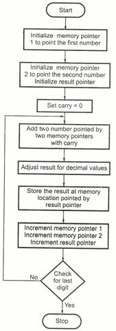
34 FLOWCHART
35 28 Statement: Add 2 arrays having ten 8-bit numbers each and generate a third array of result. It is necessary to add the first element of array 1 with the first element of array-2 and so on. The starting addresses of array l, array2 and array3 are 2200H, 2300H and 2400H, respectively. Source Program: LXI H, 2200H : Initialize memory pointer 1 LXI B, 2300H : Initialize memory pointer 2 LXI D, 2400H : Initialize result pointer BACK: LDAX B : Get the number from array 2 ADD M : Add it with number in array 1 STAX D : Store the addition in array 3 INX H : Increment pointer 1 INX B : Increment pointer2 INX D : Increment result pointer MOV A, L CPI 0AH : Check pointer 1 for last number JNZ BACK : If not, repeat : Stop

36 29 Statement: Write an assembly language program to separate even numbers from the given list of 50 numbers and store them in the another list starting from 2300H. Assume starting address of 50 number list is 2200H. Source Program: LXI H, 2200H : Initialize memory pointer l LXI D, 2300H : Initialize memory pointer2 MVI C, 32H : Initialize counter BACK:MOV A, M : Get the number ANI 0lH : Check for even number JNZ SKIP : If ODD, don't store MOV A, M : Get the number STAX D : Store the number in result list INX D : Increment pointer 2 SKIP: INX H : Increment pointer l DCR C : Decrement counter JNZ BACK : If not zero, repeat : Stop
37 30 Statement: Write assembly language program with proper comments for the following: A block of data consisting of 256 bytes is stored in memory starting at 3000H. This block is to be shifted (relocated) in memory from 3050H onwards. Do not shift the block or part of the block anywhere else in the memory. Source Program: Two blocks ( FF and F) are overlapping. Therefore it is necessary to transfer last byte first and first byte last. MVI C, FFH LX I H, 30FFH LXI D, 314FH BACK: MOV A, M STAX D DCX H DCX DCR C JNZ BACK : Initialize counter : Initialize source memory pointer 3l4FH : Initialize destination memory pointer : Get byte from source memory block : Store byte in the destination memory block : Decrement source memory pointer : Decrement destination memory pointer : Decrement counter : If counter 0 repeat : Stop execution 31 Statement: Add even parity to a string of 7-bit ASCII characters. The length of the string is in memory location 2040H and the string itself begins in memory location 2041H. Place even parity in the most significant bit of each character. Source Program: LXI H, 2040H MOV C,M : Counter for character REPEAT:INX H : Memory pointer to character MOV A,M : Character in accumulator ORA A : ORing with itself to check parity. JPO PAREVEN : If odd parity place ORI 80H even parity in D7 (80). PAREVEN:MOV M, A : Store converted even parity character. DCR C : Decrement counter. JNZ REPEAT : If not zero go for next character. : Terminate program execution
38
39 32 Statement: A list of 50 numbers is stored in memory, starting at 6000H. Find number of negative, zero and positive numbers from this list and store these results in memory locations 7000H, 7001H, and 7002H respectively. Source Program: LXI H, 6000H : Initialize memory pointer MVI C, 00H : Initialize number counter MVI B, 00H : Initialize negative number counter MVI E, 00H : Initialize zero number counter BEGIN:MOV A, M : Get the number CPI 00H : If number = 0 JZ ZERONUM : Goto zeronum ANI 80H : If MSB of number = 1i.e. if JNZ NEGNUM number is negative goto NEGNUM INR D : otherwise increment positive number counter JMP LAST ZERONUM:INR E : Increment zero number counter JMP LAST NEGNUM:INR B : Increment negative number counter LAST:INX H : Increment memory pointer INR C : Increment number counter MOV A, C CPI 32H : If number counter = 5010 then JNZ BEGIN : Store otherwise check next number LXI H, 7000 : Initialize memory pointer. MOV M, B : Store negative number. INX H MOV M, E : Store zero number. INX H MOV M, D : Store positive number. : Terminate execution
40
41 33 Statement:Write an 8085 assembly language program to insert a string of four characters from the tenth location in the given array of 50 characters. Solution: Step 1: Move bytes from location 10 till the end of array by four bytes downwards. Step 2: Insert four bytes at locations 10, 11, 12 and 13. Source Program: LXI H, 2l31H : Initialize pointer at the last location of array. LXI D, 2l35H : Initialize another pointer to point the last location of array after insertion. AGAIN: MOV A, M : Get the character STAX D : Store at the new location DCX D : Decrement destination pointer DCX H : Decrement source pointer MOV A, L : [check whether desired CPI 05H bytes are shifted or not] JNZ AGAIN : if not repeat the process INX H : adjust the memory pointer LXI D, 2200H : Initialize the memory pointer to point the string to be inserted REPE: LDAX D : Get the character MOV M, A : Store it in the array INX D : Increment source pointer INX H : Increment destination pointer MOV A, E : [Check whether the 4 bytes CPI 04 are inserted] JNZ REPE : if not repeat the process : stop 34 Statement:Write an 8085 assembly language program to delete a string of 4 characters from the tenth location in the given array of 50 characters. Solution: Shift bytes from location 14 till the end of array upwards by 4 characters i.e. from location 10 onwards. Source Program: LXI H, 2l0DH array. LXI D, 2l09H array. MOV A, M STAX D INX D INX H MOV A, L CPI 32H JNZ REPE :Initialize source memory pointer at the 14thlocation of the : Initialize destn memory pointer at the 10th location of the : Get the character : Store character at new location : Increment destination pointer : Increment source pointer : [check whether desired bytes are shifted or not] : if not repeat the process : stop
42 35 Statement:Multiply the 8-bit unsigned number in memory location 2200H by the 8-bit unsigned number in memory location 2201H. Store the 8 least significant bits of the result in memory location 2300H and the 8 most significant bits in memory location 2301H. Sample problem: (2200) = 1100 (0CH) (2201) = 0101 (05H) Multiplicand = 1100 (1210) Multiplier = 0101 (510) Result = 12 x 5 = (6010) Source program LXI H, 2200 : Initialize the memory pointer MOV E, M : Get multiplicand MVI D, 00H : Extend to 16-bits INX H : Increment memory pointer MOV A, M : Get multiplier LXI H, 0000 : Product = 0 MVI B, 08H : Initialize counter with count 8 MULT: DAD H : Product = product x 2 RAL JNC SKIP : Is carry from multiplier 1? DAD D : Yes, Product =Product + Multiplicand SKIP: DCR B : Is counter = zero JNZ MULT : no, repeat SHLD 2300H : Store the result : End of program
43
44 36 Statement:Divide the 16-bit unsigned number in memory locations 2200H and 2201H (most significant bits in 2201H) by the B-bit unsigned number in memory location 2300H store the quotient in memory location 2400H and remainder in 2401H. Assumption: The most significant bits of both the divisor and dividend are zero. Source program MVI E, 00 : Quotient = 0 LHLD 2200H : Get dividend LDA 2300 : Get divisor MOV B, A : Store divisor MVI C, 08 : Count = 8 NEXT: DAD H : Dividend = Dividend x 2 MOV A, E RLC MOV E, A : Quotient = Quotient x 2 MOV A, H SUB B : Is most significant byte of Dividend > divisor JC SKIP : No, go to Next step MOV H, A : Yes, subtract divisor INR E : and Quotient = Quotient + 1 SKIP:DCR C : Count = Count - 1 JNZ NEXT : Is count =0 repeat MOV A, E STA 2401H : Store Quotient Mov A, H STA 2410H : Store remainder : End of program.
45
46 37 Statement:Assume the DAA instruction is not present. Write a sub routine which will perform the same task as DAA. Sample Problem: Execution of DAA instruction: 1. If the value of the low order four bits (03-00) in the accumulator is greater than 9 or if auxiliary carry flag is set, the instruction adds 6 '(06) to the low-order four bits. 2. If the value of the high-order four bits (07-04) in the accumulator is greater than 9 or if carry flag is set, the instruction adds 6(06) to the high-order four bits. Source Program: LXI SP, 27FFH : Initialize stack pointer MOV E, A : Store the contents of accumulator ANI 0FH : Mask upper nibble CPI 0A H : Check if number is greater than 9 JC SKIP : if no go to skip MOV A, E : Get the number ADI 06H : Add 6 in the number JMP SECOND : Go for second check SKIP: PUSH PSW : Store accumulator and flag contents in stack POP B : Get the contents of accumulator in B register and flag register contents in C register MOV A, C : Get flag register contents in accumulator ANI 10H : Check for bit 4 JZ SECOND : if zero, go for second check MOV A, E : Get the number ADI 06 : Add 6 in the number SECOND: MOV E, A : Store the contents of accumulator ANI FOH : Mask lower nibble RRC RRC RRC RRC : Rotate number 4 bit right CPI 0AH : Check if number is greater than 9 JC SKIPl : if no go to skip 1 MOV A, E : Get the number ADI 60 H : Add 60 H in the number JMP LAST : Go to last SKIP1: JNC LAST : if carry flag = 0 go to last MOV A, E : Get the number ADI 60 H : Add 60 H in the number LAST: Note: To check auxiliary carry flag it is necessary to get the flag register contents in one of the registers and then we can check the auxiliary carry flag by checking bit 4 of that register. To get the flag register contents in any general purpose register we require stack operation and therefore stack pointer is initialized at the beginning of the source program.
47
48 38 Statement:To test RAM by writing '1' and reading it back and later writing '0' (zero) and reading it back. RAM addresses to be checked are 40FFH to 40FFH. In case of any error, it is indicated by writing 01H at port 10H. Source Program: LXI H, 4000H : Initialize memory pointer BACK: MVI M, FFH : Writing '1' into RAM MOV A, M : Reading data from RAM CPI FFH : Check for ERROR JNZ ERROR : If yes go to ERROR INX H : Increment memory pointer MOV A, H CPI SOH : Check for last check JNZ BACK : If not last, repeat LXI H, 4000H : Initialize memory pointer BACKl: MVI M, OOH : Writing '0' into RAM MOV A, M : Reading data from RAM CPI OOH : Check for ERROR INX H : Increment memory pointer MOV A, H CPI SOH : Check for last check JNZ BACKl : If not last, repeat : Stop Execution 39 Statement:Write an assembly language program to generate fibonacci number. Source Program: MVI D, COUNT MVI B, 00 MVI C, 01 MOV A, B BACK: ADD C MOV B, C MOV C, A DCR D JNZ BACK : Initialize counter : Initialize variable to store previous number : Initialize variable to store current number :[Add two numbers] :[Add two numbers] : Current number is now previous number : Save result as a new current number : Decrement count : if count 0 go to BACK : Stop. 40 Statement:Write a program to generate a delay of 0.4 sec if the crystal frequency is 5 MHz. Calculation: In 8085, the operating frequency is half of the crystal frequency, ie.operating frequency = 5/2 = 2.5 MHz Time for one T -state = Number of T-states required = = 1 x 10⁶ Source Program: LXI B, count : 16 - bit count BACK: DCX B : Decrement count MOV A, C ORA B : Logically OR Band C JNZ BACK : If result is not zero repeat
49 41 Statement: Arrange an array of 8 bit unsigned no in descending order Source Program: START:MVI B, 00 ; Flag = 0 LXI H, 4150 ; Count = length of array MOV C, M DCR C ; No. of pair = count -1 INX H ; Point to start of array LOOP:MOV A, M ; Get kth element INX H CMP M ; Compare to (K+1) th element JNC LOOP 1 ; No interchange if kth >= (k+1) th MOV D, M ; Interchange if out of order MOV M, A ; DCR H MOV M, D INX H MVI B, 01H ; Flag=1 LOOP 1:DCR C ; count down JNZ LOOP ; DCR B ; is flag = 1? JZ START ; do another sort, if yes ; If flag = 0, step execution 42 Statement: Transfer ten bytes of data from one memory to another memory block. Source memory block starts from memory location 2200H where as destination memory block starts from memory location 2300H. Source Program: LXI H, 4150 : Initialize memory pointer MVI B, 08 : count for 8-bit MVI A, 54 LOOP : RRC JC LOOP1 MVI M, 00 : store zero it no carry JMP COMMON LOOP2: MVI M, 01 : store one if there is a carry COMMON: INX H DCR B : check for carry JNZ LOOP : Terminate the program
50 43 Statement: Program to calculate the factorial of a number between 0 to 8 Source program LXI SP, 27FFH ; Initialize stack pointer LDA 2200H ; Get the number CPI 02H ; Check if number is greater than 1 JC LAST MVI D, 00H ; Load number as a result MOV E, A DCR A MOV C,A ; Load counter one less than number CALL FACTO ; Call subroutine FACTO XCHG ; Get the result in HL SHLD 2201H ; Store result in the memory JMP END LAST: LXI H, 000lH ; Store result = 01 END: SHLD 2201H Subroutine Program: FACTO:LXI H, 0000H MOV B, C ; Load counter BACK: DAD D DCR B JNZ BACK ; Multiply by successive addition XCHG ; Store result in DE DCR C ; Decrement counter CNZ FACTO ; Call subroutine FACTO RET ; Return to main program
51
52 44 Statement:Write a program to find the Square Root of an 8 bit binary number. The binary number is stored in memory location 4200H and store the square root in 4201H. Source Program: LDA 4200H : Get the given data(y) in A register MOV B,A : Save the data in B register MVI C,02H : Call the divisor(02h) in C register CALL DIV : Call division subroutine to get initial value(x) in D- reg REP: MOV E,D : Save the initial value in E-reg MOV A,B : Get the dividend(y) in A-reg MOV C,D : Get the divisor(x) in C-reg CALL DIV : Call division subroutine to get initial value(y/x) in D- reg MOV A, D : Move Y/X in A-reg ADD E : Get the((y/x) + X) in A-reg MVI C, 02H : Get the divisor(02h) in C-reg CALL DIV : Call division subroutine to get ((Y/X) + X)/2 in D- reg.this is XNEW MOV A, E : Get Xin A-reg CMP D : Compare X and XNEW JNZ REP : If XNEW is not equal to X, then repeat STA 4201H : Save the square root in memory : Terminate program execution Subroutine: DIV: MVI D, 00H NEXT:SUB C INR D CMP C JNC NEXT RET : Clear D-reg for Quotient : Subtact the divisor from dividend : Increment the quotient : Repeat subtraction until the : divisor is less than dividend : Return to main program Note: The square root can be taken y an iterative technique. First, an initial value is assumed. Here, the initial value of square root is taken as half the value of given number. Te new value of square root is computed by using an expression XNEW = (X + Y/X)/2 where, X is the initial value of square root and Y is the given number. Then, XNEW is compared wit initial value. If they are not equal then the above process is repeated until X is equal to XNEW after taking XNEW as initial value. (i.e., X XNEW)
53 Flowchart Main program Flowchart subroutine
54 45 Statement:Write a simple program to Split a HEX data into two nibbles and store it in memory Source Program: LXI H, 4200H : Set pointer data for array MOV B,M : Get the data in B-reg MOV A,B : Copy the data to A-reg ANI OFH : Mask the upper nibble INX H : Increment address as 4201 MOV M,A : Store the lower nibble in memory MOV A,B : Get the data in A-reg ANI FOH : Bring the upper nibble to lower nibble position RRC RRC RRC RRC INX H MOV M,A : Store the upper nibble in memory : Terminate program execution
55 46 Statement: Add two 4 digit BCD numbers in HL and DE register pairs and store result in memory locations, 2300H and 2301H. Ignore carry after 16 bit. Sample Problem: (HL) =3629 (DE) =4738 Step 1 : = 61 and auxiliary carry flag = 1 :.add = 67 Step 2 : (carry of LSB) = 7D Lower nibble of addition is greater than 9, so add 6. 7D + 06 = 83 Result = 8367 Source program MOV A, L : Get lower 2 digits of no. 1 ADD E : Add two lower digits DAA : Adjust result to valid BCD STA 2300H : Store partial result MOV A, H : Get most significant 2 digits of number ADC D : Add two most significant digits DAA : Adjust result to valid BCD STA 2301H : Store partial result : Terminate program execution.
56
57 47 Statement: Subtract the BCD number stored in E register from the number stored in the D register. Source Program: MVI A,99H SUB E : Find the 99's complement of subtrahend INR A : Find 100's complement of subtrahend ADD D : Add minuend to 100's complement of subtrahend DAA : Adjust for BCD : Terminate program execution Note: When two BCD numbers are subtracted, we can use DAA instruction for ajusting the result to BCD. Therefore, the subtraction of BCD number is carried out 10's complement or 100's complement. The 10's complement of a decimal number is equal to the 99's complement plus 1. The 99's complement of a number can be found by subtracting the number from 99. The steps for finding 100's complement BCD subtraction are : Find the 100's complement of subtrahend Add two numbers using BCD adition 48 Statement: Write an assembly language program to multiply 2 BCD numbers Source Program: MVI C, Multiplier : Load BCD multiplier MVI B, 00 : Initialize counter LXI H, 0000H : Result = 0000 MVI E, multiplicand : Load multiplicand MVI D, 00H : Extend to 16-bits BACK: DAD D : Result Result + Multiplicand MOV A, L : Get the lower byte of the result ADI, 00H DAA : Adjust the lower byte of result to BCD. MOV L, A : Store the lower byte of result MOV A, H : Get the higher byte of the result ACI, 00H DAA : Adjust the higher byte of the result to BCD MOV H, A : Store the higher byte of result. MOV A, B : [Increment ADI 01H : counter DAA : adjust it to BCD and MOV B,A : store it] CMP C : Compare if count = multiplier JNZ BACK : if not equal repeat : Stop

58 49 Statement:Write a program for displaying binary up counter. Counter should count numbers from 00 to FFH and it should increment after every 0.5 sec. Assume operating frequency of 8085 equal to 2MHz. Display routine is available. Source Program: LXI SP, 27FFH MVI C, OOH BACK: CALL Display CALL Delay INR C MOV A, C CPI OOH JNZ BACK : Initialize stack pointer : Initialize counter : Call display subroutine : Call delay subroutine : Increment counter : Check counter is > FFH : If not, repeat : Stop Delay Subroutine: Delay: LXI B, count : Initialize count BACK: DCX D : Decrement count MOV A, E ORA D : Logically OR D and E JNZ BACK : If result is not 0 repeat RET : Return to main program
59 Program flowchart Delay routine flowchart
60 50 Statement:Write a program for displaying BCD up counter. Counter should count numbers from 00 to 99H and it should increment after every 1 sec. Assume operating frequency of 8085 equal to 3MHz. Display routine is available. Source Program: LXI SP, 27FFH : Initialize stack pointer MVI C, OOH : Initialize counter BACK: CALL Display : Call display subroutine CALL Delay : Call delay subroutine MOV A, C ADI A, 0 1 : Increment counter DAA : Adjust it for decimal MOV C,A : Store count CPI,00 : Check count is > 99 JNZ BACK : If not, repeat : Stop Delay Subroutine: Delay:MVI B, Multiplier-count : Initialize multiplier count BACK 1:LXI D, Initialize Count BACK: DCX D : Decrement count MOV A, E ORA D : Logically OR D and E JNZ BACK : If result is not a, repeat DCR B : Decrement multiplier count JNZ BACK 1 : If not zero, repeat RET : Return to main program. Operating Frequency : 3MHz
61 Source program flowchart Routine flowchart
62 51 Statement:Write a program for displaying BCD down counter. Counter should count numbers from 99 to 00 and it should increment after every 1 sec. Assume operating frequency of 8085 equal to 3MHz. Display routine is available Source Program 1: LXI SP, 27FFH : Initialize stack pointer MVI C, 99H : Initialize counter = 99 BACK:CALL Display : Call display subroutine CALL Delay : Call delay subroutine ADI 99H : See Addition below DAA : Adjust for decimal CPI 99H : Compare with last count JNZ BACK :If no, repeat Source Program2: LXI SP, 27FFH : Initialize stack pointer MVI C, 99H : Initialize counter = 99 BACK: CALL Display : Call display subroutine CALL Delay : Call delay subroutine MOV A, C : Get count ANI 0FH : Check for lower nibble JNZ SKIP : If it is not 0FH go to skip MOV A,C : Else get the count SBI,06 : Subtract 06 MOV C,A : Store the count DCR C : Decrement count CPI 99H : Check it for last count JNZ BACK : If not, repeat : Stop
63 52 Statement:Write assembly language program to with proper comments for the following: To display decimal decrementing counter (99 to 00) at port 05 H with delay of half seconds between.each count. Write as well the delay routine giving delay of half seconds. Operating frequency of microprocessor is MHz. Neglect delay for the main program. Source Program: MVI C, 99H BACK: MOV A, C ANI OF CPI OF JNZ SKIP MOV A, C SUI 06 MOV D, A SKIP: MOV A, C OUT 05 CALL Delay DCR C MOV A, C CPI FF JNZ BACK : Initialize counter : Mask higher nibble : Subtract 6 to adjust decimal count : send count on output port : Wait for 0.5 seconds : decrement count : If not zero, repeat : Stop execution Delay subroutine: Delay: LXI D, Count Back: DCX D MOV A, D ORA E JNZ Back RET : 6 T-states : 4 T-states : 4 T-states : 10 T-states
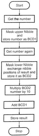
64 53 Statement:The delay routine given below is in infinite loop, identify the error and correct the program. Delay routine with error: DELAY : LXI H, N L1 : DCX H JNZ L1 Sol.: 1) The fault in the above program is at instruction JNZ L1. This condition always evaluates to be true hence loops keep on executing and hence infinite loop. 2) Reason for infinite looping: - The instruction DCX H decrease the HL pair count one by one but it does not affect the zero flag. So when count reaches to OOOOH in HL pair zero flag is not affected and JNZ L1 evaluates to be true and loop continues. Now HL again decrements below OOOOH and HL becomes FFFFH and thus execution continues. 3) The modification in the program is as follows: DELAY : LXI H, N :Load 16 bit count L1 : DCX H : Decrement count MOV A, L ORA H : logically OR Hand L JNZ L1 : If result is not 0 repeat 54 Statement: Convert a 2-digit BCD number stored at memory address 2200H into its binary equivalent number and store the result in a memory location 2300H. Sample Problem (2200H) = 67H (2300H) = 6 x OAH + 7 = 3CH + 7 = 43H Source Program: LDA 2200H : Get the BCD number MOV B, A : Save it ANI OFH : Mask most significant four bits MOV C, A : Save unpacked BCDI in C register MOV A, B : Get BCD again ANI FOH : Mask least significant four bits RRC : Convert most significant four bits into unpacked BCD2 RRC RRC RRC MOV B, A : Save unpacked BCD2 in B register XRA A : Clear accumulator (sum = 0) MVI D, 0AH : Set D as a multiplier of 10 Sum: ADD D : Add 10 until (B) = 0 DCR B : Decrement BCD2 by one JNZ SUM : Is multiplication complete? i if not, go back and add again ADD C : Add BCD1 STA 2300H : Store the result : Terminate program execution
65
66 55 Statement: Write a main program and a conversion subroutine to convert the binary number stored at 6000H into its equivalent BCD number. Store the result from memory location 6100H. Sample Problem: (6000) H = 8AH 3 1.8AH? 64H (Decimal 100) :. Divide by 64H (Decimal 100) 8AH/64H? Quotient = 1, Remainder = 26H 26H < 64H (Decimal 100) :. Go to step 2 and Digit 2 = H? OAH (Decimal 10) :. Divide by OAH (Decimal 10) 26H/OAH? Quotient = 3, Remainder = O8H OSH < OAH (Decimal 10) :. Go to step 3 and Digit 1 = 3. Digit 0 = O8H Source Program: LXI SP, 27FFH LDA 6000H CALL SUBROUTINE : Initialize stack pointer : Get the binary number in accumulator : Call subroutine : Terminate program execution Subroutine to convert binary number into its equivalent BCD number: PUSH B : Save BC register pair contents PUSH D : Save DE register pair contents MVI B, 64H : Load divisor decimal 100 in B register MVI C, 0AH : Load divisor decimal 10 in C register MVI D, 00H : Initialize Digit 1 MVI E, 00H : Initialize Digit 2 STEP1: CMP B : Check if number < Decimal 100 JC STEP 2 : if yes go to step 2 SUB B : Subtract decimal 100 INR E : update quotient JMP STEP 1 : go to step 1 STEP2: CMP C : Check if number < Decimal 10 JC STEP 3 : if yes go to step 3 SUB C : Subtract decimal 10 INR D : Update quotient JMP STEP 2 : Continue division by 10 STEP3: STA 6100H : Store Digit 0 MOV A, D : Get Digit 1 STA 6101H : Store Digit 1 MOV A, E : Get Digit 2 STA 6102H : Store Digit 2 POP D : Restore DE register pair POP B : Restore BC register pair RET : Return to main program
67
68 56 Statement: Find the 7-segment codes for given 5 numbers from memory location 6000H and store the result from memory location 7000H. Sample Problem: (6000) H = 8AH Source Program LXI H, 6200H LXI D, 6000H LXI B, 7000H BACK: LDAX D MOV L, A MOV A, M STAX B INX D INX B MOV A, C CPI O5H JNZ BACK : Initialize lookup table pointer : Initialize source memory pointer : Initialize destination memory pointer : Get the number : A point to the 7-segment code : Get the 7-segment code : Store the result at destination memory location : Increment source memory pointer : Increment destination memory pointer : Check for last number : If not repeat : End of program
69 57 Statement: Write an assembly language program to convert the contents of the five memory locations starting from 2000H into an ASCII character. Place the result in another five memory locations starting from 2200H. Sample Problem (2000H) = 1 (2001H) = 2 (2002H) = 9 (2003H) = A (2004H) = B Result:(2200H) = 31 (2201H) = 32 (2202H) = 39 (2203H) = 41 (2204H) = 42 Source program: LXI SP, 27FFH : Initialize stack pointer LXI H, 2000H : Source memory pointer LXI D, 2200H : Destination memory pointer MVI C, O5H : Initialize the counter BACK: MOV A, M : Get the number CALL ASCII : Call subroutine ASCII STAX D : Store result INX H : Increment source memory pointer INX D : Increment destination memory pointer DCR C : Decrement count by 1 CJNZ : if not zero, repeat : Stop program execution subroutine ASCII ASCII: CPI, OAH : Check if number is OAR JNC NEXT : If yes go to next otherwise continue ADI 30H JMP LAST NEXT: ADI 37H LAST: RET : Return to main program Subroutine: Subroutine 'ASCII' converts a hexadecimal digit to ASCII.The digit is passed using accumulator and the result is stored in accumulator.stack starts From 27FEH to 27FDH. Note: The ASCII Code (American Standard Code for Information Interchange) is commonly used for communication. In such cases we need to convert binary number to its ASCII equivalent. It is a seven bit code. In this code number 0 through 9 are represented as 30 through 39 respectively and letters A through Z are represented as 41H through 5AH. Therefore, by adding 30H we can convert number into its ASCII equivalent and by adding 37H we can convert letter to its ASCII equivalent.
70
71 58 Statement: convert the ASCII number in memory to its equivalent decimal number Source Program: LXI H, 4150 : Point to data MOV A, M : Get operand SUI 30 : convert to decimal CPI 0A : Check whether it is valid decimal number JC LOOP : yes, store result MVI A, FF : No, make result=ff LOOP: INX H MOV M, A : (A) = (4151) Note: The ASCII Code (American Standard Code for Information Interchange) is commonly used for communication. It is a seven bit code. In this code number 0 through 9 are represented as 30 through 39 respectively and letters A through Z are represented as 41H through 5AH. Therefore, by subtracting 30H we can convert an ASCII number into its decimal equivalent.
72 59 Statement: Convert the HEX number in memory to its equivalent decimal number Source Program: LXI H, 4150 LXI B, 0000 MOV A, M LOOP: SUI 64 JC LOOP 1 INR B JMP LOOP LOOP 1: ADI 64 LOOP 2: SUI 0A JC LOOP 3 INR C JMP LOOP 2 LOOP 3: ADI 0A INX H MOV M, B MOV B, A MOV A, C RLC RLC RLC RLC ADD B INX H MOV M, A ; Point to data ; Initialize hundreds= 0, Tens=0 ; Get hex data to A ; hundreds= hundreds+1 ; if subtracted extra, add it clear carry flag ; Tens=tens+1 ; If subtracted extra, add it again ; A = Units ; store hundreds ; Combine Tens in C & ; Units in A to form a ; Single 8-bit number ; Store tens & Units Note: In this experiment the number is converted to its equivalent decimal number using the following logic. First count the number of hundreds, the number of tens & units present in that hex number. Then add up to get the equivalent decimal number. Converting A9 we get: A9 /64=45 Hundreds = 01 Since 64(100 decimal) cannot be subtracted from 45 no. of hundreds = 01. Now count tens 45/0A=3B Tens = 01 Now from 09, 0A cannot be subtracted. Hence tens = 06 the decimal equivalent of A9 is 169.
73 60 Statement: Convert an 8 bit hex no to its binary form & store in memory. Source Program: LXI H, 4150 : Initialize memory pointer MVI B, 08 : count for 8-bit MVI A, 54 LOOP : RRC JC LOOP1 MVI M, 00 : store zero it no carry JMP COMMON LOOP2: MVI M, 01 : store one if there is a carry COMMON: INX H DCR B : check for carry JNZ LOOP : Terminate the program 61 Statement: Write a program to output contents of B register LSB to MSB on the SOD pin. Source program: MVI C, 08H : Initialize count with 8 MOV A, B BACK: RRC : Rotate B register contents right MOV B, A : Save contents of register B JNC SKIP : If no carry skip MVI A, COH SIM : If carry, send high on SOD JMP NEXT SKIP: MVI A, 40H SIM : If no carry, send low on SOD. NEXT: CALL DELAY : Wait for specific time DCR C : Decrement count by 1 JNZ BACK : if count = 0 Stop, if not repeat : Stop program execution Delay subroutine: Delay: LXI D, Count Back: DCX D MOV A, D ORA E JNZ Back RET
74
75 62 Statement: Write a program to output square wave of 1 khz frequency on the SOD pinof 8085 for 5 seconds. Operating frequency of 8085 is 2 MHz. Source program LXI SP, 27FFH : Initialize stack pointer LXI B, 1388H : Initialize counter with count BACK: MVI A, COH SIM : Send high on SOD pin CALL DELAY : Wait for 0.5 msec MVI A, 40H : Send low on SOD pin CALL DELAY : wait for. 5 msec DCX B : Decrement count by 1 MOV A, C ORA B : Check if count = 0 JNZ BACK : If not, repeat : Stop program execution Delay subroutine: Delay: LXI D, Count Back: DCX D MOV A, D ORA E JNZ Back RET
76
77 63 Statement: An ASCII character is being received on SID pin of Write a program in assembly language of 8085 to assemble this character and store it in memory. Write comment for each instruction. Source program: LXI SP, 27FFH LXI H, 2000H RIM ANI 80H CALL Delay MVI B, 08H MVI D, 00H UP1: ALL Delay RIM ANI 80H ORA D RRC MOV D, A DCR B JNZ UP1 RLC MOV M, A RIM ANI 8OH CZ error Delay subroutine: : Memory pointer : Read SID : Check D7 bit of Accumulator : 1/2 bit time delay for stop bit : Initialize bit counter : Clear data register : 1 bit time : Read SID line : Mask bits B6 - Bo : OR data bit with previous bits : Store data bit at appropriate position : Shift left to correct result : Store result : Read stop bit : If not stop bit call error : Terminate program. Delay: LXI D, Count Back: DCX D MOV A, D ORA E JNZ Back RET
78
79 64 Statement: Write a assembly program to transmit a message from an 8085 to a CRT terminal for the following requirements and draw the interfacing diagram. i) A message of 50 characters is stored as ASCII characters (without parity) in memory locations starting at 2200H. ii) Baud rate x 16 iii) Stop bits 2 Solution Description: CRT terminal uses normal RS 232C standard serial communication interface. Therefore, to transmit data to CRT it is necessary to have RS 232C interface at the sending end. Fig. shows the interfacing of 8251 with RS 232C to As shown in the Fig. three RS-232C signals (TxD, RxD are Ground) are used for serial communication between the CRT terminal and the 8085 system. Line drivers and receivers are used to transfer logic levels from TTL logic to RS-232C logic. For RS-232C the voltage level +3V to +15V is defined as logic 0 and voltage level from -3V to -15V is defined as logic 1. The line driver, MC 1488, converts logic 1 of TIL to approximately -9V and logic a of TIL to approximately +9V. These levels at the receiving end are again converted by the line receiver, MC1489, into TTL compatible logic.
80 Source program: LXI H, 2200H MVI C, 32H MVI A, 00H OUT FFH OUT FFH OUT FFH MVI A, 40H OUT FFH MVI A, CAH OUT FFH MVI A, 11H OUT FFH CHECK: IN FFH ANI 0lH JZ CHECK MOV A, M OUT FEH INX H DCR C JNZ CHECK : Initialize memory pointer to pointer the message : Initialize counter to send 50 characters : Dummy mode word : Reset command word : Reset 8251A : Mode word initialization : Command word initialization : Check TxRDY : Is TxRDY I? if not, check again : Get the character in accumulator : Send character to the transmitter : Increment memory pointer : Decrement counter : if not zero, send next character : Stop program execution
81
82 65 Statement: Write a assembly program to receive 25 bytes from an CRT terminal to 8085 for the following requirements. i) Baud rate x 16 ii) Stop bits 2 Note: Reading of status word is necessary for checking the status of RxD line of 8085 that whether receiver is ready to give data or not. Source program: LXI H, 2300 H MVI C, FFH MVI A, 00H OUT FFH OUT FFH OUT FFH MVI A, 40H OUT FFH MVI A, CAH OUT FFH MVI A, 14 H OUT FFH CHECK: IN FFH ANI 02 H JZ CHECK : Initialize memory pointer : Initialize counter to accept 25 characters : Dummy mode word : Reset command word : Reset 8251 A : Mode word initialization : Command word initialization : Check RxRDY : Is RxRDY? If not, check again
83 IN FEH : Get the character MOV M, A : save the character INX H : Increment memory pointer DCR C : Decrement memory pointer OUT FEH : Send character to the transmitter JNZ CHECK : If not zero, accept next character : Stop program execution
84 66 Statement: Write a program to initialize 8255 in the configuration given below Sample 1: Write a program to initialize 8255 in the configuration given below: 1. Port A: Simple input 2. Port B: Simple output 3. Port CL: Output 4. Port Cu: Input Assume address of the control word register of 8255 as 83H. Solution: SOURCE PROGRAM 1: MVI A, 98H OUT 83H : Load control word : Send control word Sample 2: Write a program to initialize 8255 in the configuration given below: 1. Port A: Output with handshake 2. Port B: Input with handshake 3. Port CL: Output 4. Port Cu: Input Assume address of the control word register of 8255 as 23H. Solution: SOURCE PROGRAM 2: MVI A, AEH OUT 23H : Load control word : Send control word

85 67 Statement: Write a program to blink Port C bit 0 of the Assume address of control word register of 8255 as 83H. Use Bit Set/Reset mode. Source program: BACK: MVI A, 0lH OUT 83H CALL DELAY MVI A, 00H OUT 83H CALL Delay JMP BACK Delay subroutine: : Load bit pattern to make PCο high : Send it to control word register : Call Delay subroutine : Load bit pattern to make PCο Low : Send it to control word register : Call Delay subroutine : Repeat Delay: LXI D, Count Back: DCX D MOV A, D ORA E JNZ Back RET
86 68 Statement: Design a system (both Software and Hardware) that will cause 4 LEDs to flash 10 times when a push button switch is pressed. Use Assume persistence of vision to be 0.1 seconds. Source program: LXI SP, 2000 H : Initialize stack pointer MVI A, 90H OUT CR : Initialize 8255 BACK: IN PA : [Read status ANI 01 : of push JNZ BACK : button] MVI B, 0AH : Initialize counter AGAIN: MVI A, 00H : Load data to light LEDs OUT PC : Send data on port C CALL Delay : Call. Delay of 0.1 sec MVI A, FFH : Load data to switch off LEDs OUT PC : Send data on port C CALL Delay : Call Delay of 0.1 sec DCR B : Decrement count JNZ AGAIN : If not zero repeat JMP BACK : Jump back to read status Delay subroutine: Delay: LXI D, Count Back: DCX D MOV A, D ORA E JNZ Back RET
 Allow traffic from W to E and E to W transition for 20 seconds.")
87 69 Statement: Design a microprocessor system to control traffic lights. The traffic light arrangement is as shown in Fig. The traffic should be controlled in the following manner. 1) Allow traffic from W to E and E to W transition for 20 seconds. 2) Give transition period of 5 seconds (Yellow bulbs ON) 3) Allow traffic from N to 5 and 5 to N for 20 seconds 4) Give transition period of 5 seconds (Yellow bulbs ON) 5) Repeat the process. HARDWARE FOR TRAFFIC LIGHT CONTROL Fig. shows the interfacing diagram to control 12 electric bulbs. Port A is used to control lights on N-S road and Port B is used to control lights on W-E road. Actual pin connections are listed in Table 1 below. The electric bulbs are controlled by relays. The 8255 pins are used to control relay on-off action with the help of relay driver circuits. The driver circuit includes 12 transistors to drive 12 relays. Fig. also shows the interfacing of 8255 to the system.
88 INTERFACING DIAGRAM SOFTWARE FOR TRAFFIC LIGHT CONTROL
89 Source program: MVI A, 80H OUT 83H (CR) START: MVI A, 09H OUT 80H (PA) MVI A, 24H OUT 81H (PB) MVI C, 28H CALL DELAY MVI A, 12H OUT (81H) PA OUT (81H) PB MVI C, 0AH CALL: DELAY MVI A, 24H OUT (80H) PA MVI A, 09H OUT (81H) PB MVI C, 28H CALL DELAY MVI A, 12H OUT PA OUT PB MVI C, 0AH CALL DELAY JMP START : Initialize 8255, port A and port B : in output mode : Send data on PA to glow R1 and R2 : Send data on PB to glow G3 and G4 : Load multiplier count (40ıο) for delay : Call delay subroutine : Send data on Port A to glow Y1 and Y2 : Send data on port B to glow Y3 and Y4 : Load multiplier count (10ıο) for delay : Call delay subroutine : Send data on port A to glow G1 and G2 : Send data on port B to glow R3 and R4 : Load multiplier count (40ıο) for delay : Call delay subroutine : Send data on port A to glow Y1 and Y2 : Send data on port B to glow Y3 and Y4 : Load multiplier count (10ıο) for delay : Call delay subroutine Delay Subroutine: DELAY: LXI D, Count : Load count to give 0.5 sec delay BACK: DCX D : Decrement counter MOV A, D ORA E : Check whether count is 0 JNZ BACK : If not zero, repeat DCR C : Check if multiplier zero, otherwise repeat JNZ DELAY RET : Return to main program
90
91 70 Statement: Interface a Stepper Motor to the 8085 microprocessor system and write an 8085 assembly language program to control the Stepper Motor. HARDWARE FOR STEPPER MOTOR CONTROL A stepper motor is a digital motor. It can be driven by digital signal. Fig. shows the typical 2 phase motor rated 12V /0.67 A/ph interfaced with the 8085 microprocessor system using Motor shown in the circuit has two phases, with center-tap winding. The center taps of these windings are connected to the 12V supply. Due to this, motor can be excited by grounding four terminals of the two windings. Motor can be rotated in steps by giving proper excitation sequence to these windings. The lower nibble of port A of the 8255 is used to generate excitation signals in the proper sequence. These excitation signals are buffered using driver transistors. The transistors are selected such that they can source rated current for the windings. Motor is rotated by 1.80 per excitation. INTERFACING SCHEME SOFTWARE FOR STEPPER MOTOR CONTROL As port A is used as an output port, control word for 8255 is 80H. Stepper Motor Control Program: rotation 6000H Excite code DB 03H, 06H, 09H, OCH : This is the code sequence for clockwise
92 Subroutine to rotate a stepper motor clockwise by Set the counts: MVI C, 32H START: MVI B, 04H LXI H, 6000H BACK1: MOV A, M OUT PORTA CALL DELAY INX H DCR B JNZ BACK l DCR C JNZ START RET : Set repetition count to 50ıο : Counts excitation sequence : Initialize pointer : Get the Excite code : Send Excite code : Wait : Increment pointer : Repeat 4 times : Repeat 50 times Delay subroutine: Delay: LXI D, Count Back: DCX D MOV A, D ORA E JNZ Back RET
93 71 Statement: Interface a 64-key matrix keyboard to the 8085 microprocessor using Write an 8085 assembly language program to initialize 8255 and to read the key code. HARDWARE FOR MATRIX KEYBOARD INTERFACE Fig. shows a matrix keyboard with 64 keys connected to the 8085 microprocessor using A matrix keyboard reduces the number of connections, thus the number of interfacing lines. In this example, the keyboard with 64 keys, is arranged in 8 x 8 (8 rows and 8 columns) matrix. This requires sixteen lines from the microprocessor to make all the connections instead of 64 lines if the keys are connected individually. The interfacing of matrix keyboard requires two ports: one input port and other output port. Rows are connected to the input port, port A and columns are connected to the output port, port B. INTERFACING SCHEME Source program MVI A, 90H OUT CR START: MVI A, 00 OUT PB BACK: IN PA CPI FF JNZ BACK CALL DELAY BACK 1: IN PA SOFTWARE FOR MATRIX KEYBOARD INTERFACE : Initialize Port A as input and : Port B as Output : Make all scan lines zero : Check for key release : If not, wait for key release : Wait for key debounce
94 CPI FF : Check for key press JZ BACK 1 : If not, wait for key press CALL DELAY : Wait for key debounce MVI L, 00H : Initialize key counter MVI C, 08H MVI B, FEH : Make one column low NEXTCOL: MOV A, B OUT PB MVI D, 08H : Initialize row counter IN PA : Read return line status NEXTROW: RRC : Check for one row JNC DISPLAY : If zero, goto display else continue INR L : Increment key counter DCR D : Decrement row counter JNZ NEXTROW : Check for next row MOV A, B RLC : Select the next column MOV B, A DCR C : Decrement column count JNZ NEXTCOL : Check for last column if not repeat JMP START : Go to start Delay subroutine: Delay: LXI D, Count Back: DCX D MOV A, D ORA E JNZ Back RET

95
96 72 Statement: Interface an 8-digit 7 segment LED display using 8255 to the 8085 microprocessor system and write an 8085 assembly language routine to display message on the display. HARDWARE FOR EIGHT DIGIT SEVEN SEGMENT DISPLAY INTERFACE Fig. shows the multiplexed eight 7-segment display connected in the 8085 system using In this circuit port A and port B are used as simple latched output ports. Port A provides the segment data inputs to the display and port B provides a means of selecting a display position at a time for multiplexing the displays. A0-A7 lines are used to decode the addresses for For this circuit different addresses are: PA = 00H PB = 01H PC = 02H CR = 03H. The register values are chosen in Fig. such that the segment current is 80 ma. This current is required to produce an average of 10 ma per segment as the displays are multiplexed. In this type of display system, only one of the eight display position is 'ON' at any given instant. Only one digit is selected at a time by giving low signal on the corresponding control line. Maximum anode current is 560 ma (7-segments x 80 ma = 560 ma), but the average anode current is 70 ma. INTERFACING SCHEME
97 SOFTWARE FOR EIGHT DIGIT SEVEN SEGMENT DISPLAY INTERFACE For 8255, Port A and B are used as output ports. The control word format of 8255 according to hardware connections is: Source program: SOFTWARE TO INITIALIZE 8255: MVI A, 80H : Load control word in AL OUT CR : Load control word in CR SUBROUTINE TO DISPLAY MESSAGE ON MULTIPLEXED LED DISPLAY: SET UP REGISTERS FOR DISPLAY: MVI B, 08H MVI C, 7FH LXI H, 6000B : load count : load select pattern : starting address of message DISPLAY MESSAGE: DISP 1: MOV A, C OUT PB MOV A, M OUT PA CALL DELAY DISP 1: MOV A, C RRC MOV C, A INX H DCR B JNZ DISP 1 RET : select digit : get data : display data : wait for some time : adjust selection pattern : Decrement count : repeat 8 times Note: This "display message subroutine" must be called continuously to display the 7-segment coded message stored in the memory from address 6000H. Delay subroutine: Delay: LXI D, Count Back: DCX D MOV A, D ORA E JNZ Back RET
98 73 Statement: Interface an 8 x 8 matrix keyboard to 8085 through 8279 in 2-key lockout mode and write an assembly language program to read keycode of the pressed key. The external clock frequency is 2MHz. Use I/O mapped I/O technique. (Dont use any Interrupts) HARDWARE FOR 8 x 8 MATRIX KEYBOARD INTERFACE SOFTWARE FOR 8 x 8 MATRIX KEYBOARD INTERFACE SOFTWARE FOR 8 x 8 MATRIX KEYBOARD INTERFACE The three steps needed to write the software are: Step 1: Find keyboard/display command word. Step 2: Find program clock command word

99 Step 3: Find Read FIFO/sensor RAM command word. Source program: MVI A, 00H OUT 81H MVI A, 34H OUT 81H BACK: IN 81H ANI 07H JZ BACK RAM MVI A, 40H OUT 81H IN 80H : Initialize keyboard/display : in encoded scan keyboard-2 keylockout mode : Initialize prescaler count : Read FIFO status word : Mask bit B3 to B7 : If 0, key is not pressed wait for key press else read FIFO : Initialize 8279 in read : FI FO RAM mode : Read FIFO RAM (keycode) : Stop program execution. FLOWCHART
100 74 Statement: Interface an 8 x 8 matrix keyboard to 8085 through 8279 in 2-key lockout mode and write an assembly language program to read keycode of the pressed key. The external clock frequency is 2MHz. Use I/O mapped I/O technique. HARDWARE FOR 8 x 8 MATRIX KEYBOARD INTERFACE(With Interrupt) Fig. shows the interfacing of 8 x 8 matrix keyboard in interrupt driven keyboard mode. In the interrupt driven mode interrupt line from 8279 is connected to the one of the interrupt input of 8085 except INTR. Here, INT line from 8279 is connected to the interrupt RST 7.5 of Other signal connections are same as in the non interrupt mode. SOFTWARE FOR 8 x 8 MATRIX KEYBOARD INTERFACE(With Interrupt) The three steps needed to write the software are: Step 1: Find keyboard/display command word.
101 Step 2: Find program clock command word Step 3: Find Read FIFO/sensor RAM command word. Source program: MVI A, 00H : Initialize keyboard/display in encoded OUT 81H : scan keyboard 2 key lockout mode MVI A, 34H OUT 81H : Initialize prescaler count MVI A, 0BH : Load mask pattern to enable RST 7.5 SIM : mask other interrupts EI : Enable Interrupt HERE: JMP HERE : Wait for the interrupt Interrupt Subroutine: MVI A, 40H : Initialize 8279 in read FIFO OUT 81H : RAM mode IN 80H : Read FIFO RAM (keycode) EI : Enable Interrupt RET : Return to main program Note: In the interrupt driven keyboard, when key is pressed, key code is loaded into FIFO RAM and interrupt is generated. This interrupt signal is used to tell CPU that there is a keycode in the FIFO RAM. CPU then initiates read command with in the interrupt service routine to read key code from the FIFO RAM. FLOWCHART
102 75 Statement: Interface an 8 x 4 matrix keyboard to 8085 through HARDWARE FOR INTERFACING 8x4 MATRIX KEYBOARD NOTE: As keyboard is having 8 rows and 4 columns, only 4 scan lines are required and we can avoid external decoder to generate scan lines by selecting decoded scan keyboard mode. SOFTWARE FOR INTERFACING 8x4 MATRIX KEYBOARD Source program: MVI A, 00H : Initialize keyboard/display in encoded OUT 81H : scan keyboard 2 key lockout mode MVI A, 34H OUT 81H : Initialize prescaler count MVI A, 0BH : Load mask pattern to enable RST 7.5 SIM : mask other interrupts EI : Enable Interrupt HERE: JMP HERE : Wait for the interrupt Interrupt Subroutine: MVI A, 40H : Initialize 8279 in read FIFO OUT 81H : RAM mode IN 80H : Read FIFO RAM (keycode) EI : Enable Interrupt RET : Return to main program
103 76 Statement: Interface 8/7-segment digits (common cathode) to 8085 through 8279 and write an 8085 assembly language program to display 1 to 8 on the eight seven segment digits. External clock frequency is 3 MHz. HARDWARE FOR EIGHT SEVEN SEGMENT DIGITS INTERFACE Fig. shows the interfacing of eight 7-segment digits to 8085 through As shown in the figure eight display lines (Bo-B3 and Ao-A3) are buffered with the help of transistor and used to drive display digits. These buffered lines are connected in parallel to all display digits. So, Sl and S2 lines are decoded and decoded lines are used for selection of one of the eight digits. SOFTWARE FOR EIGHT SEVEN SEGMENT DIGITS INTERFACE To display 1 to 8 numbers on the eight 7-segment digits we have to load 7- segment codes for 1 to 8 numbers in the corresponding display locations. The three steps needed to write the software are: Step 1: Find keyboard/display command word.

104 Step 2: Find program clock command word Step 3: Find display RAM command word. Source program: LXI B, 6200B MVI C, 08H MVI A, 00H OUT 8IH MVI A, 3EH OUT 8IH MVI A, 90H OUT 8IH BACK : MOV A, M OUT 80H INX H DCR C JNZ BACK : Initialize lookup table pointer : Initialize counter : Initialize keyboard/display : Mode : Initialize prescaler count : Initial size 8279 in write Display : RAM-mode : Get the 7-segment code : Write 7-segment code in display RAM : Increment lookup table pointer : Decrement counter : if count = 0 stop, otherwise go to back : Stop program execution LOOK UP TABLE FLOWCHART
EXAMPLE PROGRAMS 8085
 P! EXAMPLE PROGRAMS 8085 Statement:Multiply the 8-bit unsigned number in memory location 2200H by the 8-bit unsigned number in memory location 2201H. Store the 8 least significant bits of the result in
(2) Explain the addressing mode of OR What do you mean by addressing mode? Explain diff. addressing mode for 8085 with examples.
 Explain the addressing mode of OR What do you mean by addressing mode? Explain diff. addressing mode for 8085 with examples.") (1) Explain instruction format and Opcode format of 8085 μp with example. OR With help of examples, explain the formation of opcodes of 8085 OR What is an instruction? List type of instruction based on
(1) Explain instruction format and Opcode format of 8085 μp with example. OR With help of examples, explain the formation of opcodes of 8085 OR What is an instruction? List type of instruction based on
 Instruction Set Instruction set of 8085 can be classified in following groups: Data Transfer Instructions These instructions can perform data transfer operations between Registers of 8085 e.g. MOV 8085
Practical Course File For
 Practical Course File For Microprocessor (IT 473) B.Tech (IT) IV-SEM Department of IT University Institute of Engineering & Technology Panjab University, Chandigarh Page 1 INTRODUCTION... 4 EXPERIMENT-1:
8085 INSTRUCTION SET INSTRUCTION DETAILS
 8085 INSTRUCTION SET INSTRUCTION DETAILS DATA TRANSFER INSTRUCTIONS MOV Rd, Rs Copy from source to destination This instruction copies the contents of the source register Rs into the destination register
Introduction to Assembly Language Programming (Instruction Set) 1/18/2011 1
 1/18/2011 1") Introduction to Assembly Language Programming (Instruction Set) 1/18/2011 1 High Level Language Compiler Assembly Language Assembler Machine Code Microprocessor Hardware 1/18/2011 2 8085A Instruction Set
Introduction to Assembly Language Programming (Instruction Set) 1/18/2011 1 High Level Language Compiler Assembly Language Assembler Machine Code Microprocessor Hardware 1/18/2011 2 8085A Instruction Set
INSTRUCTION SET OF 8085
 INSTRUCTION SET OF 8085 Instruction Set of 8085 An instruction is a binary pattern designed inside a microprocessor to perform a specific function. The entire group of instructions that a microprocessor
MAHALAKSHMI ENGINEERING COLLEGE TIRUCHIRAPALLI
 MAHALAKSHMI ENGINEERING COLLEGE TIRUCHIRAPALLI-621213. QUESTION BANK DEPARTMENT: EEE SUB CODE: EE2324 YR/ SEM:III/ VI SUB NAME: MICROPROCESSORS & MICROCONTROLLERS UNIT 2- PROGRAMMING OF 8085 MICROPROCESSORS
Assembly Language Programming of 8085
 Assembly Language Programming of 8085 1. Introduction A microprocessor executes instructions given by the user Instructions should be in a language known to the microprocessor Microprocessor understands
Assembly Language Programming of 8085
 Assembly Language Programming of 8085 Topics 1. Introduction 2. Programming model of 8085 3. Instruction set of 8085 4. Example Programs 5. Addressing modes of 8085 6. Instruction & Data Formats of 8085
Assembly language Programming
 Assembly language Programming Applications With out the assembly language programming microprocessor can not works. Instructions are the patterns which is require by the microprocessor to done any task.
Its Assembly language programming
 8085 Architecture & Its Assembly language programming Dr A Sahu Dept of Computer Science & Engineering IIT Guwahati 8085 Era and Features 8085 Outline Block diagram (Data Path) Bus Structure Register Structure
LIST OF PROGRAMS. Prg. Name of the Program. 1 Study of Pin Diagram of Study of Architecture of Study of 8085 Kit.
 LIST OF PROGRAMS Prg. Name of the Program No. 1 Study of Pin Diagram of 8085 2 Study of Architecture of 8085 3 Study of 8085 Kit 4 Reverse Order 5 Exchange of memory blocks 6 Absolute Difference 7 Even
UNIT 1 REFERENCE 1 PREPARED BY S.RAVINDRAKUMAR, LECT/ECE, CHETTINAD COLLEGE OF ENGG AND TECH, KARUR
 UNIT 1 REFERENCE 1 PROGRAMMING THE 8085 DEVELOPMENT OF PROGRAM A program is a sequence of instructions written to tell a computer to perform a specific function. The instructions are selected from the
SAMPLE STUDY MATERIAL
 Microprocessor-IN Postal Correspondence Course 1 SAMPLE STUDY MATERIAL Instrumentation Engineering IN Postal Correspondence Course GATE & PSUs Microprocessor Microprocessor-IN Postal Correspondence Course
Subject Code: Model Answer Page No: /25
 Important Instructions to examiners: 1) The answers should be examined by key words and not as word-to-word as given in the model answer scheme. 2) The model answer and the answer written by candidate
Delhi Noida Bhopal Hyderabad Jaipur Lucknow Indore Pune Bhubaneswar Kolkata Patna Web: Ph:
 Serial :. PT_EE-EC_A_Microprocessor_968 Delhi Noida Bhopal Hyderabad Jaipur Lucknow Indore Pune Bhubaneswar Kolkata Patna Web: E-mail: info@madeeasy.in Ph: -452462 CLASS TEST 28-9 Subject : Microprocessors
SIR C.R.REDDY COLLEGE OF ENGINEERING ELURU DIGITAL ELECTRONICS & MICROPROCESSOR LAB MANUAL 2/4 CSE: II- SEMESTER
 SIR C.R.REDDY COLLEGE OF ENGINEERING ELURU 534007 DEPARTMENT OF COMPUTER SCIENCE AND ENGINEERING DIGITAL ELECTRONICS & MICROPROCESSOR LAB MANUAL 2/4 CSE: II- SEMESTER Faculty: B.Homer Benny (Section- A
Unit 1 8 BIT MICROPROCESSOR ARCHITECTURE
 Unit 1 8 BIT MICROPROCESSOR ARCHITECTURE 8085 -Internal Architecture - Addressing modes - Instruction set -Timing diagrams -Interrupts-Assembly language Programming 1. Internal Architecture of 8085 Microprocessor
م.م. ماجد عيدان. Introduction to microprocessor and microcomputer
 Lect. (1) Introduction to microprocessor and microcomputer Reference Books: 1. Ramesh S. Gaonkar, "Microprocessor Architecture, Programming and Application with the 8085". 2. Anokh Singh, A.K. Chhabra,Fundamentals
ELECTRICAL ENGINEERING
 Serial : 1. JP_EE_Microprocessor_130618 CLASS TEST Delhi Noida Bhopal Hyderabad Jaipur Lucknow Indore Pune Bhubaneswar Kolkata Patna Web: E-mail: info@madeeasy.in Ph: 011-45124612 ELECTRICAL ENGINEERING
Delhi Noida Bhopal Hyderabad Jaipur Lucknow Indore Pune Bhubaneswar Kolkata Patna Web: Ph:
 Serial : 01. ND_EE_NW_Microprocessors_150718 Delhi Noida Bhopal Hyderabad Jaipur Lucknow Indore Pune Bhubaneswar Kolkata Patna Web: E-mail: info@madeeasy.in Ph: 011-45124612 CLASS TEST 2018-19 ELECTRICAL
MSMF GATE CENTRE. Sub: MICROPROCESSORS. Time: 50min Date: Marks:33
 MSMF GATE CENTRE Sub: MICROPROCESSORS Time: 50min Date:20-12-16 Marks:33 1. Which interrupt has highest priority in 8085 microprocessor? a) INTR b) RST 4.5 c) RST 6.5 d) RST 7.5 2. In 8085 microprocessor,
LABORATORY MANUAL. PROGRAMME: B.Tech SEMESTER /YEAR: 3rd year 5th Semester SUBJECT CODE: CS592 SUBJECT NAME: Microprocessor & Microcontroller Lab
 LABORATORY MANUAL PROGRAMME: B.Tech SEMESTER /YEAR: 3rd year 5th Semester SUBJECT CODE: CS592 SUBJECT NAME: Microprocessor & Microcontroller Lab DEPARTMENT OF COMPUTER SCIENCE & ENGINEERING INSTITUTE OF
CS2259-MICROPROCESSOR AND MICROCONTROLLER LABORATORY MANUAL
 CS2259-MICROPROCESSOR AND MICROCONTROLLER LABORATORY LABORATORY MANUAL FOR IV SEMESTER B.TECH / IT ACADEMIC YEAR: 2012-2013 (FOR PRIVATE CIRCULATION ONLY) ANNA UNIVERSITY, CHENNAI. NAME REG.NO BATCH :
 Contents 8051 Instruction Set BY D. BALAKRISHNA, Research Assistant, IIIT-H Chapter I : Control Transfer Instructions Lesson (a): Loop Lesson (b): Jump (i) Conditional Lesson (c): Lesson (d): Lesson (e):
Architecture & Instruction set of 8085 Microprocessor and 8051 Micro Controller
 of 8085 microprocessor 8085 is pronounced as "eighty-eighty-five" microprocessor. It is an 8-bit microprocessor designed by Intel in 1977 using NMOS technology. It has the following configuration 8-bit
Programming of 8085 microprocessor and 8051 micro controller Study material
 8085 Demo Programs Now, let us take a look at some program demonstrations using the above instructions Adding Two 8-bit Numbers Write a program to add data at 3005H & 3006H memory location and store the
UNIT I. Differences between: Microcomputer, Microprocessor and Microcontroller
 UNIT I SYLLABUS INTRODUCTION TO 8085 Intel 8085 Microprocessor architecture signals Addressing modes Instruction classification Instruction set Timing diagram ALP format Programming 8085 8-bit and 16-bit
INSTITUTE OF ENGINEERING AND MANAGEMENT, KOLKATA Microprocessor
 INSTITUTE OF ENGINEERING AND MANAGEMENT, KOLKATA Microprocessor Subject Name: Microprocessor and Microcontroller Year: 3 rd Year Subject Code: CS502 Semester: 5 th Module Day Assignment 1 Microprocessor
SIR.C.R.R.COLLEGE OF ENGINEERING DEPT. OF ELECTRONICS AND INSTRUMENTATION ENGG. EIE-328: MICROPROCESSOR LABORATORY 3/4 B.E. EIE: SECOND SEMESTER
 SIR.C.R.R.COLLEGE OF ENGINEERING DEPT. OF ELECTRONICS AND INSTRUMENTATION ENGG. EIE-328: MICROPROCESSOR LABORATORY 3/4 B.E. EIE: SECOND SEMESTER (AS PER UNIVERSITY SYLLABUS) LIST OF EXPERIMENTS 1. UNDERSTANDING
MAHARASHTRA STATE BOARD OF TECHNICAL EDUCATION (Autonomous) (ISO/IEC Certified) MODEL ANSWER
 (ISO/IEC Certified) MODEL ANSWER") MODEL ANSWER SUMMER 17 EXAMINATION Subject Title: Microprocessor Subject Code: 17443 I m p o r t a n t I n s t r u c t i o n s t o e x a m i n e r s : 1) The answers should be examined by key words and
MODEL ANSWER SUMMER 17 EXAMINATION Subject Title: Microprocessor Subject Code: 17443 I m p o r t a n t I n s t r u c t i o n s t o e x a m i n e r s : 1) The answers should be examined by key words and
GATE Exercises on Microprocessors
 1 GATE Exercises on Microprocessors Abstract This problem set has questions taken from GATE papers over the last twenty years. Teachers can use the problem set for courses tutorials. 1) The clock frequency
Valliammai Engineering College
 Valliammai Engineering College SRM Nagar, Kattankulathur - 603203 Department of Electrical and Electronics Engineering EE6612 Microprocessors and Microcontrollers Laboratory LAB MANUAL VI Semester - Electrical
G. Pullaiah College of Engineering and Technology: Kurnool Department Of Electronics and Communication Engineering
 G. Pullaiah College of Engineering and Technology: Kurnool Department Of Electronics and Communication Engineering LECTURE NOTES MICROPROCESSORS AND INTERFACING PREPARED BY V.SHANTHI ASST PROFESSOR DEPT
Principle and Interface Techniques of Microcontroller
 Principle and Interface Techniques of Microcontroller --8051 Microcontroller and Embedded Systems Using Assembly and C LI, Guang ( 李光 ) Prof. PhD, DIC, MIET WANG, You ( 王酉 ) PhD, MIET 杭州 浙江大学 2011 Chapter
The 8085 Instruction Set
 1 of 8 2/9/2011 5:14 PM The 8085 Instruction Set As I promised, in an earlier lesson, I am going to go through an in-depth explaination of ALL the 8085 instructions. Intel 88888 000 88888 5555555 A 8 8
MAHALAKSHMI ENGINEERING COLLEGE TIRUCHIRAPALLI UNIT I THE 8085 & 8086 MICROPROCESSORS. PART A (2 Marks)
") MAHALAKSHMI ENGINEERING COLLEGE TIRUCHIRAPALLI-621213. UNIT I THE 8085 & 8086 MICROPROCESSORS PART A (2 Marks) 1. Give the significance of SIM and RIM instruction available in 8085. [NOV/DEC 2006] Instruction
MAHALAKSHMI ENGINEERING COLLEGE TIRUCHIRAPALLI-621213. UNIT I THE 8085 & 8086 MICROPROCESSORS PART A (2 Marks) 1. Give the significance of SIM and RIM instruction available in 8085. [NOV/DEC 2006] Instruction
1 = Enable SOD 0 = Disable SOD. Serial Output Data. Fig.12.9 SIM Instruction Format
 Lecture-67 The 8085 Serial I/O Lines: SOD & SID The 8085 microprocessor has two pins specially designed for software control serial I/O. One is called SOD (serial output data) and the other is called SID
8051 Overview and Instruction Set
 8051 Overview and Instruction Set Curtis A. Nelson Engr 355 1 Microprocessors vs. Microcontrollers Microprocessors are single-chip CPUs used in microcomputers Microcontrollers and microprocessors are different
ET355 Microprocessors Thursday 6:00 pm 10:20 pm
 ITT Technical Institute ET355 Microprocessors Thursday 6:00 pm 10:20 pm Unit 4 Chapter 6, pp. 139-174 Chapter 7, pp. 181-188 Unit 4 Objectives Lecture: BCD Programming Examples of the 805x Microprocessor
Instruction set of 8085
 Instruction set of 05 /23/2016 ptkarule@rediffmail.com 1 Instruction set of 05 Instruction set is divided into various groups depending on the operations performed: 1. Data transfer 2. rithmetic 3. Logical
COPYRIGHT IS NOT RESERVED BY AUTHORS. AUTHORS ARE NOT RESPONSIBLE FOR ANY LEGAL ISSUES ARISING OUT OF ANY COPYRIGHT DEMANDS
 COPYRIGHT IS NOT RESERVED BY AUTHORS. AUTHORS ARE NOT RESPONSIBLE FOR ANY LEGAL ISSUES ARISING OUT OF ANY COPYRIGHT DEMANDS AND/OR REPRINT ISSUES CONTAINED IN THIS MATERIALS. THIS IS NOT MEANT FOR ANY
EE309: Computer Organization, Architecture and MicroProcessors. sumantra/courses/up/up.html GND HIGH ORDER ADDRESS BUS
 CMP:8085 Primer-1 EE309: Computer Organization, rchitecture and MicroProcessors http://www.ee.iitb.ac.in/ sumantra/courses/up/up.html The 8085 Chip F LGS: S Z x x P x cy EXTERNLLY INITITED SIGNLS SERIL
MGM S Jawaharlal Nehru Engineering College
 MGM S Jawaharlal Nehru Engineering College Laboratory Manual MICROPROCESSOR AND INTERFACING TECHNIQUES For TE (EEP) Prof.J.R.Rana Author JNEC, Aurangabad PREFACE It is my great pleasure to present this
UNIT 2 THE 8051 INSTRUCTION SET AND PROGRAMMING
 UNIT 2 THE 8051 INSTRUCTION SET AND PROGRAMMING Instructions Alphabetical List of Instructions ACALL: Absolute Call ADD, ADDC: Add Accumulator (With Carry) AJMP: Absolute Jump ANL: Bitwise AND CJNE: Compare
8051 Programming: Arithmetic and Logic
 8051 Programming: Arithmetic and Logic EE4380 Fall 2002 Class 4 Pari vallal Kannan Center for Integrated Circuits and Systems University of Texas at Dallas Topics Signed and Unsigned arithmetic Binary
DHANALAKSHMI COLLEGE OF ENGINEERING DEPARTMENT OF ELECTRICAL AND ELECTRONICS ENGINEERING YEAR : III SEM : VI
 DHANALAKSHMI COLLEGE OF ENGINEERING DEPARTMENT OF ELECTRICAL AND ELECTRONICS ENGINEERING YEAR : III SEM : VI EE2354- MICROPROCESSORS AND MICROCONTROLLER UNIT I 8085 and 8086 PROCESSOR PART A 1. Define
Microcontroller Intel [Instruction Set]
![Microcontroller Intel [Instruction Set]](/thumbs/82/86620819.jpg "Microcontroller Intel [Instruction Set]") Microcontroller Intel 8051 [Instruction Set] Structure of Assembly Language [ label: ] mnemonic [operands] [ ;comment ] Example: MOV R1, #25H ; load data 25H into R1 2 8051 Assembly Language Registers
Microcontroller Intel 8051 [Instruction Set] Structure of Assembly Language [ label: ] mnemonic [operands] [ ;comment ] Example: MOV R1, #25H ; load data 25H into R1 2 8051 Assembly Language Registers
(2½ Hours) [Total Marks: 75]
![(2½ Hours) [Total Marks: 75]](/thumbs/76/73743076.jpg "(2½ Hours) [Total Marks: 75]") (2½ Hours) [Total Marks: 75] N. B.: (1) All questions are compulsory. (2) Make suitable assumptions wherever necessary and state the assumptions made. (3) Answers to the same question must be written together.
(2½ Hours) [Total Marks: 75] N. B.: (1) All questions are compulsory. (2) Make suitable assumptions wherever necessary and state the assumptions made. (3) Answers to the same question must be written together.
SN8F5000 Family Instruction Set
 SONiX Technology Co., Ltd. 8051-based Microcontroller 1 Overview SN8F5000 is 8051 Flash Type microcontroller supports comprehensive assembly instructions and which are fully compatible with standard 8051.
Microprocessors 1. The 8051 Instruction Set. Microprocessors 1 1. Msc. Ivan A. Escobar Broitman
 Microprocessors 1 The 8051 Instruction Set Microprocessors 1 1 Instruction Groups The 8051 has 255 instructions Every 8-bit opcode from 00 to FF is used except for A5. The instructions are grouped into
Matrix Multiplication in 8085
 Matrix Multiplication in 8085 Semester Project for B.Tech. (Computer Science & Engineering) by Praneeth A S (UG20110023) & Rohit Yeravothula (UG201110039) Project Guide: Dr. K R Chowdhary Head of Department,
EXPERIMENT NO. 1 THE MKT 8085 MICROPROCESSOR TRAINER
 OBJECT: EXPERIMENT NO. 1 THE MKT 8085 MICROPROCESSOR TRAINER To understand the structure and operating instruction of the microprocessor trainer. INTRODUCTION: The MKT 8085 is a single-board microcomputer,
CHAPTER 6 ARITHMETIC, LOGIC INSTRUCTIONS, AND PROGRAMS
 CHAPTER 6 ARITHMETIC, LOGIC INSTRUCTIONS, AND PROGRAMS Addition of Unsigned Numbers The instruction ADD is used to add two operands Destination operand is always in register A Source operand can be a register,
Memory organization Programming model - Program status word - register banks - Addressing modes - instruction set Programming examples.
 MICROCONTROLLERS AND APPLICATIONS 1 Module 2 Module-2 Contents: Memory organization Programming model - Program status word - register banks - Addressing modes - instruction set Programming examples. MEMORY
The due date for submitting this assignment has passed. 1) How many times will the following loop be executed? Depends on the initial value of A
 How many times will the following loop be executed? Depends on the initial value of A") X reviewer2@nptel.iitm.ac.in Courses» and Microcontrollers Unit 4 - Week 3 Announcements Course Ask a Question Progress Mentor Course outline How to access the portal Week 3 Assignment The due date for
X reviewer2@nptel.iitm.ac.in Courses» and Microcontrollers Unit 4 - Week 3 Announcements Course Ask a Question Progress Mentor Course outline How to access the portal Week 3 Assignment The due date for
EXPERIMENT-1 AIM: Familiarization of different keys of 8085 microprocessor kit and its memory map. APPARATUS: 8085 kit. DIAGRAM:
 EXPERIMENT-1 AIM: Familiarization of different keys of 8085 microprocessor kit and its memory map. APPARATUS: 8085 kit. DIAGRAM: Reset VCT INT Shift C D E F RTG SI INSD DELD 8 9 A B DEL GO INS BM REL EMEM
DEPARTMENT OF COMPUTER SCIENCE AND ENGINEERING LAB MANUAL. Academic Year: ODD SEMESTER
 DEPARTMENT OF COMPUTER SCIENCE AND ENGINEERING LAB MANUAL Academic Year: 2015-16 ODD SEMESTER Programme (UG/PG) : UG-B.Tech Semester : 03 Course Code Course Title :CS1033 : MICROPROCESSOR & INTERFACING
Computer Organization
 Computer Organization (Instruction set Architecture & Assembly Language Programming) KR Chowdhary Professor & Head Email: kr.chowdhary@gmail.com webpage: krchowdhary.com Department of Computer Science
Intel 8086: Instruction Set
 IUST-EE (Chapter 6) Intel 8086: Instruction Set 1 Outline Instruction Set Data Transfer Instructions Arithmetic Instructions Bit Manipulation Instructions String Instructions Unconditional Transfer Instruction
EC 333 Microprocessor and Interfacing Techniques (3+1)
") EC 333 Microprocessor and Interfacing Techniques (3+1) Lecture 6 8086/88 Microprocessor Programming (Arithmetic Instructions) Dr Hashim Ali Fall 2018 Department of Computer Science and Engineering HITEC
EC 333 Microprocessor and Interfacing Techniques (3+1) Lecture 6 8086/88 Microprocessor Programming (Arithmetic Instructions) Dr Hashim Ali Fall 2018 Department of Computer Science and Engineering HITEC
PERIPHERAL INTERFACING Rev. 1.0
 This work is licensed under the Creative Commons Attribution-NonCommercial-Share Alike 2.5 India License. To view a copy of this license, visit http://creativecommons.org/licenses/by-nc-sa/2.5/in/deed.en
Microcontroller. Instruction set of 8051
 UNIT 2: Addressing Modes and Operations: Introduction, Addressing modes, External data Moves, Code Memory, Read Only Data Moves / Indexed Addressing mode, PUSH and POP Opcodes, Data exchanges, Example
1. Internal Architecture of 8085 Microprocessor
 Practical 1 Date : AIM : Introduction Of Microprocessor 8085. 1. Internal Architecture of 8085 Microprocessor Control Unit Generates signals within µp to carry out the instruction, which has been decoded.
Arithmetic Instructions
 Segment 3C Arithmetic Instructions This topic covers the following instructions: Addition (ADD, INC, ADC) Subtraction (SUB, DEC, SBB,CMP) Multiplication (MUL, IMUL) Division (DIV, IDIV) BCD Arithmetic
EC2304-MICROPROCESSOR AND MICROCONROLLERS 2 marks questions and answers UNIT-I
 EC2304-MICROPROCESSOR AND MICROCONROLLERS 2 marks questions and answers 1. Define microprocessors? UNIT-I A semiconductor device(integrated circuit) manufactured by using the LSI technique. It includes
ROEVER ENGINEERING COLLEGE
 ROEVER ENGINEERING COLLEGE ELAMBALUR, PERAMBALUR- 621 212 DEPARTMENT OF INFORMATION TECHNOLOGY MICROPROCESSOR & MICROCONTROLLER 2 marks questions andanswers Unit I 1. Define microprocessor? A microprocessor
INDEX. 1 Study of intel 8085 micropeocessor kit. 2 Program to find addition of two 8 bit no. 3 Program to find subtraction of two 8 bit no.
 INDEX PROGRAM NO. NAME OF THE PROGRAM 1 Study of intel 8085 micropeocessor kit SIGNATURE 2 Program to find addition of two 8 bit no. 3 Program to find subtraction of two 8 bit no. 4 Program to find 1 s
The advantages of registers over memory locations are as follows:
 Q.2 a. In a microprocessor, what is the use of a register? What are the advantages & disadvantages of using registers over a memory location? What is the speciality of register A (accumulator) over other
UNIT 18 PROGRAMMING MICROPROCESSORS
 UNIT 18 PROGRAMMING MICROPROCESSORS Structure 18.1 Introduction Objectives 18.2 Computer Languages 18.2.1 High Level Languages and Compilers 18.2.2 Assembly Language and the Assembler 18.3 Microprocessor
EEE310 MICROPROCESSORS M. Fatih Tüysüz CHAPTER 7
 EEE31 MICROPROCESSORS M. Fatih Tüysüz CHAPTER 7 CHAPTER 7 Contents Midterm Questions & Solutions Serial I/O Data Transfer Midterm Questions & Solutions Q1: a) Why Microprocessors use only two digits (
8088/8086 Programming Integer Instructions and Computations
 Unit3 reference 2 8088/8086 Programming Integer Instructions and Computations Introduction Up to this point we have studied the software architecture of the 8088 and 8086 microprocessors, their instruction
VALLIAMMAI ENGINEERING COLLEGE
 VALLIAMMAI ENGINEERING COLLEGE SRM Nagar, Kattankulathur 603 203 DEPARTMENT OF ELECTRICAL AND ELECTRONICS ENGINEERING QUESTION BANK V SEMESTER EE6502- MICROPROCESSORS AND MICROCONTROLLERS Regulation 2013
EEM336 Microprocessors I. Arithmetic and Logic Instructions
 EEM336 Microprocessors I Arithmetic and Logic Instructions Introduction We examine the arithmetic and logic instructions. The arithmetic instructions include addition, subtraction, multiplication, division,
Micro Processor & Micro Controllers
 Micro Processor & Micro Controllers 1. What is microprocessor? It is a program controlled semi conductor device (IC), which fetches, decodes and execute instructions. 2. What are the basic units of microprocessor?
PERIPHERAL INTERFACING Rev. 1.0
 This work is licensed under the Creative Commons Attribution-NonCommercial-Share Alike 2.5 India License. To view a copy of this license, visit http://creativecommons.org/licenses/by-nc-sa/2.5/in/deed.en
Delhi Noida Bhopal Hyderabad Jaipur Lucknow Indore Pune Bhubaneswar Kolkata Patna Web: Ph:
 Serial : LS2_EE_S_Microprocessors_2688 Delhi Noida Bhopal Hyderabad Jaipur Lucknow Indore Pune Bhubaneswar Kolkata Patna Web: E-mail: info@madeeasy.in Ph: -452462 CLASS TEST 28-9 ELECTRICAL ENGINEERING
Microprocessor Micro Syllabus BSc. CSIT, IOST, TU. Microprocessor
 Microprocessor Micro Syllabus BSc. CSIT, IOST, TU Microprocessor Course Title: Microprocessor Full Marks: 60 + 20 + 20 Course No: CSC162 Pass Marks: 24 + 8 + 8 Nature of the Course: Theory + Lab Credit
EKT222 Miroprocessor Systems Lab 5
 LAB 5: Interrupts Objectives: 1) Ability to define interrupt in 8085 microprocessor 2) Ability to understanding the interrupt structure in the 8085 microprocessor 3) Ability to create programs using the
S.R.M. INSTITUTE OF SCIENCE & TECHNOLOGY SCHOOL OF ELECTRONICS & COMMUNICATION ENGINEERING
 S.R.M. INSTITUTE OF SCIENCE & TECHNOLOGY SCHOOL OF ELECTRONICS & COMMUNICATION ENGINEERING QUESTION BANK Subject Code : EC307 Subject Name : Microprocessor and Interfacing Year & Sem : III Year, V Sem
Module Contents of the Module Hours COs
 Microcontrollers (EE45): Syllabus: Module Contents of the Module Hours COs 1 8051 MICROCONTROLLER ARCHITECTURE: Introduction to Microprocessors and Microcontrollers, the 8051 Architecture, 08 1 and pin
Q. P. Code : b. Draw and explain the block dig of a computer with microprocessor as CPU.
 Q. P. Code : 08235 (2½ Hours) [Total Marks: 75] N. B.: (1) All questions are compulsory. (2) Make suitable assumptions wherever necessary and state the assumptions made. (3) Answers to the same question
8051 Microcontrollers
 8051 Microcontrollers Richa Upadhyay Prabhu NMIMS s MPSTME richa.upadhyay@nmims.edu March 15, 2016 8051 INSTRUCTIONS JUMP, LOOP AND CALL INSTRUCTIONS 8051 INSTRUCTIONS Repeating a sequence of instructions
UNIT THE 8051 INSTRUCTION SET AND PROGRAMMING
 UNIT THE 8051 INSTRUCTION SET AND PROGRAMMING Instructions Alphabetical List of Instructions ACALL: Absolute Call ADD, ADDC: Add Accumulator (With Carry) AJMP: Absolute Jump ANL: Bitwise AND CJNE: Compare
ELEG3923 Microprocessor Ch.6 Arithmetic and Logics
 Department of Electrical Engineering University of Arkansas ELEG3923 Microprocessor Ch.6 Arithmetic and Logics Dr. Jingxian Wu wuj@uark.edu OUTLINE 2 Arithmetic instructions Signed number operations Logic
ENE 334 Microprocessors
 Page 1 ENE 334 Microprocessors Lecture 10: MCS-51: Logical and Arithmetic : Dejwoot KHAWPARISUTH http://webstaff.kmutt.ac.th/~dejwoot.kha/ ENE 334 MCS-51 Logical & Arithmetic Page 2 Logical: Objectives
LABORATORY 1 INTRODUCTION TO 8085 MICROPROCESSOR DEVELOPMENT SYSTEM BOARD
 LABORATORY 1 INTRODUCTION TO 8085 MICROPROCESSOR DEVELOPMENT SYSTEM BOARD 1. INTRODUCTION TO 8085 MICROPROCESSOR DEVELOPMENT SYSTEMS. The basic components of the 8085 Microprocessor Development System
1. What is microprocessor? It is a program controlled semi conductor device (IC), which fetches, decodes and execute instructions.
, which fetches, decodes and execute instructions.") Downloaded from www.books4career.blogspot.com 1. What is microprocessor? It is a program controlled semi conductor device (IC), which fetches, decodes and execute instructions. 2. What are the basic units
Downloaded from www.books4career.blogspot.com 1. What is microprocessor? It is a program controlled semi conductor device (IC), which fetches, decodes and execute instructions. 2. What are the basic units
CHETTINAD COLLEGE OF ENGINEERING AND TECHNOLOGY
 CHETTINAD COLLEGE OF ENGINEERING AND TECHNOLOGY DEPARTMENT ELECTRONICS AND COMMUNICATION ENGINEERING CS 2252-MICROPROCESSOR AND MICROCONTROLLER COURSE NOTES UNIT I 8085 MICROPROCESSOR OBJECTIVES:.* Study
 Sri Krishna Engineering College Panapakkam, Chennai 601 301 Lab Manual CS2259 MICROPROCESSORS LAB Department of Electronics and Communication Engineering CS 2259 Microprocessors Lab SKEC Page 1 List of
Digital Fundamentals. CHAPTER 2 Number Systems, Operations, and Codes
 Digital Fundamentals CHAPTER 2 Number Systems, Operations, and Codes Decimal Numbers The decimal number system has ten digits: 0, 1, 2, 3, 4, 5, 6, 7, 8, and 9 The decimal numbering system has a base of
Counters & Time Delays. Microprocessors & Interfacing 1
 Counters & Time Delays Microprocessors & Interfacing 1 Counters A loop counter is set up by loading a register with a certain value Then using the DCR (to decrement) and INR (to increment) the contents
1. INTRODUCTION TO MICROPROCESSOR AND MICROCOMPUTER ARCHITECTURE:
 1. INTRODUCTION TO MICROPROCESSOR AND MICROCOMPUTER ARCHITECTURE: A microprocessor is a programmable electronics chip that has computing and decision making capabilities similar to central processing unit
BINARY SYSTEM. Binary system is used in digital systems because it is:
 CHAPTER 2 CHAPTER CONTENTS 2.1 Binary System 2.2 Binary Arithmetic Operation 2.3 Signed & Unsigned Numbers 2.4 Arithmetic Operations of Signed Numbers 2.5 Hexadecimal Number System 2.6 Octal Number System
XII HSC - BOARD - MARCH
 Date: 17.03.2018 JEE MEDICAL-UG BOARDS KVPY NTSE OLYMPIADS XII HSC - BOARD - MARCH - 2018 COMPUTER SCIENCE - II ( D-9) QP + SOLUTIONS 1. (A) Select correct options and rewrite the following : (a) Intel
1-Operand instruction types 1 INC/ DEC/ NOT/NEG R/M. 2 PUSH/ POP R16/M16/SR/F 2 x ( ) = 74 opcodes 3 MUL/ IMUL/ DIV/ DIV R/M
 = 74 opcodes 3 MUL/ IMUL/ DIV/ DIV R/M") Increment R16 1-Operand instruction types 1 INC/ DEC/ NOT/NEG R/M 4 x (16+48) = 256 opcodes 2 PUSH/ POP R16/M16/SR/F 2 x (8+24+4+1) = 74 opcodes 3 MUL/ IMUL/ DIV/ DIV R/M 4 x (16+48) = 256 opcodes INC
Increment R16 1-Operand instruction types 1 INC/ DEC/ NOT/NEG R/M 4 x (16+48) = 256 opcodes 2 PUSH/ POP R16/M16/SR/F 2 x (8+24+4+1) = 74 opcodes 3 MUL/ IMUL/ DIV/ DIV R/M 4 x (16+48) = 256 opcodes INC
B.C.A 2017 MICROPROCESSOR AND ASSEMBLY LANGUAGE MODULE SPECIFICATION SHEET. Course Outline
 B.C.A 2017 MICROPROCESSOR AND ASSEMBLY LANGUAGE Course Outline MODULE SPECIFICATION SHEET The objective of the course is to expose to the students to the architecture and instruction set of typical 8-bit
1. Internal Architecture of 8085 Microprocessor
 Practical 1 Date : AIM : Introduction Of Microprocessor 8085. 1. Internal Architecture of 8085 Microprocessor Control Unit Generates signals within µp to carry out the instruction, which has been decoded.
Arithmetic and Logic Instructions And Programs
 Dec Hex Bin 3 3 00000011 ORG ; FOUR Arithmetic and Logic Instructions And Programs OBJECTIVES this chapter enables the student to: Demonstrate how 8-bit and 16-bit unsigned numbers are added in the x86.