Introduction to DSP/FPGA Programming Using MATLAB Simulink
|
|
|
- Clinton Wilkinson
- 6 years ago
- Views:
Transcription


1 دوازدهمين سمينار ساليانه دانشكده مهندسي برق فناوری های الکترونيک قدرت اسفند 93 Introduction to DSP/FPGA Programming Using MATLAB Simulink By: Dr. M.R. Zolghadri Dr. M. Shahbazi N. Noroozi
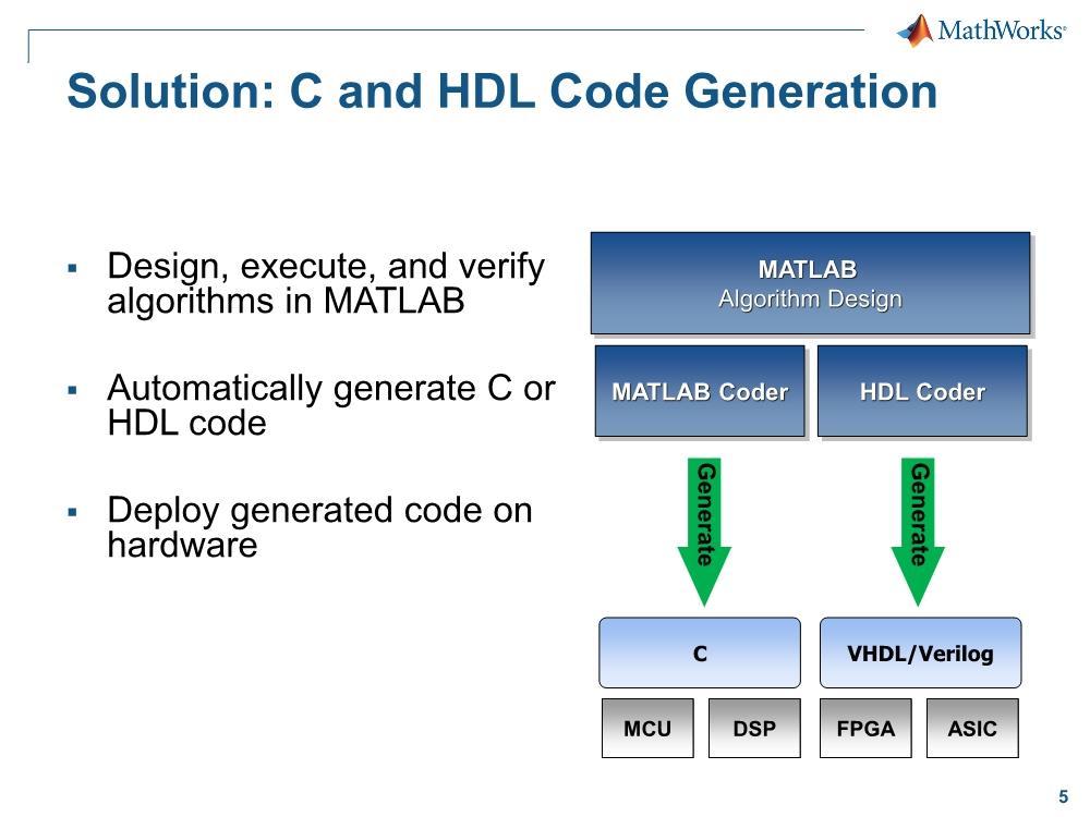
2 2 Table of main context Section III FPGA basic concepts MATLAB/Simulink for FPGA implementation Xilinx system generator Conclusion
3 3 Summary Section III Introduction to FPGA Matlab/Simulink for Model-based Design and Implementation of FPGAs Xilinx System Generator Review of Fixed-point Representation Overview of HDL Coder
4 4 History of Evolution FPGAs belong to a class of devices named as FPD(field programmable device) PLD(programmable logic devices)
 Programmable AND plane and fixed OR plane.")
5 5 PLD Programmable Logic Array (PLA): Programmable AND plane followed by programmable or wired OR plane. Sum of product form Programmable Array Logic (PAL) Programmable AND plane and fixed OR plane. Low cost and size Less flexible than PLA

6 6 PLD Part of the logic diagram of the PAL 16L8.
7 7 What s inside an FPGA Logic Clock resources Extremely high-bandwidth RAM Multipliers Lots of wire that can be connected in any fashion
8 8 FPGA vs ASIC FPGA advantages: Faster time-to-market Simpler design cycle Field programmability (easy to upgrade firmware) ASIC advantages: Full custom capabilities Lower unit cost Higher performance Not suitable in power applications
9 9 How is an FPGA programmed Write a program in HDL (VHDL, Verilog, ) Simulate Synthesis Place and route Timinig-maximum clockrate Resuting.bin file to be programmed on FPGA
10 10 Can FPGA do anything Yes and no Like a microprocessor it need a program: P IP: intellectual property You can buy parts of the program or write it entirely yourself Free IP
11 11 Challenges in FPGA design It is harder to master than micro. Design can be time consuming. In software, when you are 80% complete, you are 80% done. With FPGA when you are 80% one you are 20% through your project.
12 12 Do I need an FPGA? You may need an FPGA if: Yu need very fast interrupts You need many interrupts You have very complex operations You have many interrupt sources that should be in parallel Real-time requirements Very large bandwidth is needed
13 13 Do I need an FPGA? You have lots of logic on your PCB Replace lots of small components with an FPGA Fewer PCB spins Some operations are impossible on microcontrller

14 14 Soft CPUs An FPGA can implement a CPU ARM7/9 performance This is offered by all FPGA vendors
15 15 FPGA application Replace logic DSP Communication Video Non-standard interface
16 16 FPGA application in power electronics Time constraint High switching frequency (low voltage SMPS) Increased control quality (mimic analog controller in sensor-less EKF) Parallelism constraints (combined multiphase multilevel) Hardware in the loop application Real-time digital simulator Artificial intelligence
 Input/Output Block(IOB) - provides the interface between -external pins and internal -signal lines 3) Programmable Routing Channel -controls the connections")
17 17 FPGA architecture There are three primary configurable elements in FPGA 1) Configurable Logic Block(CLB) -implement different functions. 2) Input/Output Block(IOB) - provides the interface between -external pins and internal -signal lines 3) Programmable Routing Channel -controls the connections among different blocks
18 18 Logic Blocks Purpose: to implement combinational and sequential logic functions. Logic blocks can be implemented by: Transistor pairs Multiplexers Look up tables( LUT) Wide fan-in AND-OR structure.
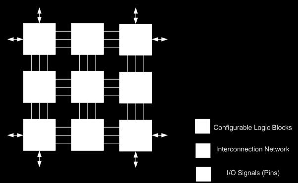

19 19 Simplified CLB Structure
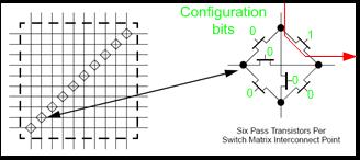
20 20 Example: 4-input AND gate A B C D O A B C D A B C D O D SET CLR Q Q MUX 0 O Configuration bits
21 21 Interconnection Network
22 22 Placement: Select CLBs Input1 Input2 CLB0 SB0 CLB1 SB1 SB2 SB3 Input3 CLB2 SB4 CLB3 Output
23 23 Routing: Select path SB1 Configuration bits Input Input2 CLB0 SB0 CLB SB1 SB2 SB3 SB4 Configuration bits Input3 CLB2 SB4 CLB3 Output
24 24 Configuration Bitstream The configuration bitstream must include ALL CLBs and SBs, even unused ones CLB0: CLB1: CLB2: XXXXX CLB3: SB0: SB1: SB2: SB3: SB4:
25 25 Summary Section III Introduction to FPGA Matlab/Simulink for Model-based Design and Implementation of FPGAs Xilinx System Generator Review of Fixed-point Representation Overview of HDL Coder
26 26 Mathworks and Xilinx Workflow MathWorks: accelerate the pace of engineering and science by providing best in class Software for: Development and verification of algorithms and control logic - development and verification of algorithms and control logic Embedded Systems implementation Xilinx: providing best in class Silicon including FPGAs and embedded system hardware platforms : Offers FPGAs and Zynq an Extensible Processing Platform Partner with MathWorks to provide an integrated workflow
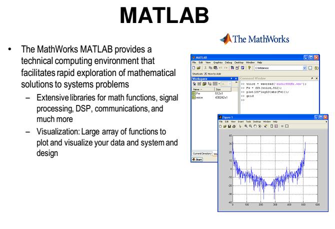
27 27 MATLAB
28 28 Simulink Simulink - Visual data flow environment for modeling and simulation of dynamical systems Fully integrated with the MATLAB engine Graphical block editor Event-driven simulator Models parallelism Extensive library of parameterizable functions Simulink Blockset - math, sinks, sources DSP Blockset - filters, transforms, etc. Communications Blockset - modulation, DPCM, etc.

29 29 Who uses Model-based Design
30 30 Why Model-based Design?
31 31 Summary Section III Introduction to FPGA Matlab/Simulink for Model-based Design and Implementation of FPGAs Xilinx System Generator Review of Fixed-point Representation Overview of HDL Coder
32 32 The Challenges for a DSP Software Platform Industry Trends Trend towards platform chips (FPGAs, DSP) resulting in greater complexity Highly flexible systems required to meet changing standards Multiple design methodologies - control plane/data-path Challenges in modeling and implementing an entire platform Hardware in the loop verification is useful in complex system design and System Generator supports it System Design Challenges Leveraging legacy HDL code Modeling & implementing control logic and datapath No expert exists for all facets of system design
33 33 Traditional approach to FPGA programming Hardware description languages (HDL) like Verilog/VHDL allow designers to specify at a higher level than logic gates high-level (=easier to understand) Simulation possibility Hard to master Challenges in modeling and implementing an entire platform The only solution for a long time
34 34 Model-based approach in FPGA programming Hardware description languages (HDL) like Verilog/VHDL allow designers to specify at a higher level than logic gates We will use an even higher level tool called System Generator Alternative for Altera FPGAs: DSPBuilder Graphical programming environment within Matlab s Simulink
35 35 System Generator Overview Industry s system-level design environment (IDE) for FPGAs Integrated design flow from Simulink to bit file Leverages existing technologies Matlab/Simulink R13.1 or R14 from The MathWorks HDL synthesis IP Core libraries FPGA implementation tools Simulink library of arithmetic, logic operators and DSP functions (Xilinx Blockset) Bit and cycle true to FPGA implementation Arithmetic abstraction Arbitrary precision fixed-point, including quantization and overflow Simulation of double precision as well as fixed point
36 36 System Generator Overview VHDL code generation for Virtex-II Pro, Virtex -II, Virtex -E, Virtex, Spartan -3, Spartan -IIE and Spartan -II devices Hardware expansion and mapping Synthesizable VHDL with model hierarchy preserved Mixed language support for Verilog Automatic invocation of CORE Generator to utilize IP cores ISE project generation to simplify the design flow HDL testbench and test vector generation Constraint file (.xcf), simulation.do files generation HDL Co-Simulation via HDL C-Simulation Verification acceleration using Hardware in the Loop
37 37 System Generator Basics System Generator provides two key tools Blocks for building your model Hardware generator: model HDL Simulink provides a test environment for your design Generate test vectors with MATLAB or Simulink blocks Visualize and analyze output of design Leverage MATLAB expressions within design Simulation and hardware will match bit true and cycle true

38 38 System Generator

39 39 System Generator Example Simulink blocks are your signal sources and sinks Xilinx blocks are your to-be-synthesized FPGA design

40 40 System Generator Example These will be realized in hardware

41 41 System Generator Example Configures simulation & hardware parameters Relates sample period to hardware clock Used to synthesize model Sets target FPGA device for model

42 42 System Generator Example Convert between floating and fixed point values Top-level ports in HDL model Must set precision & sample rate in Gateway In

43 43 System Generator Example Must be outside System Generator gateways Operate on floating point values Good for data sources & analysis Source: continuous-time floating point constant Sink: signal vs. time scope
44 44 System Generator Basics Every model needs a System Generator token Models start and end with Gateway blocks : double to fixed point conversion : fixed point to double conversion Any Simulink blocks can be used outside gateways Good for data sources and output analysis Only Xilinx blocks can be used inside gateways Synthesis treats gateways as top-level ports

45 45 Creating a System Generator Design Exactly like conventional Simulink design

46 46 Blocks Xilinx blockset has nine major sections Basic elements. Counters, delays Communication Error correction blocks Control Logic. MCode, Black Box Data Types Convert, Slice DSP.. FDATool, FFT, FIR Index. All Xilinx blocks quick way to view all blocks Math. Multiply, accumulate, inverter Memory Dual Port RAM, Single Port RAM Tools. ModelSim, Resource Estimator

47 47 Configure Blocks Double-click or go to Block Parameters to view a block s configurable parameters Arithmetic Type: Unsigned or twos complement Implement with Xilinx Smart-IP Core (if possible)/ Generate Core Latency: Specify the delay through the block Overflow and Quantization: Users can saturate or wrap overflow. Truncate or Round Quantization Override with Doubles: Simulation only Precision: Full or the user can define the number of bits and where the decimal point is for the block Sample Period: Can be inherent with a -1 or must be an integer value Note: While all parameters can be simulated, not all are realizable

48 48 Values Can Be Equations You can also enter equations in the block parameters, which can aid calculation and your own understanding of the model parameters The equations are calculated at the beginning of a simulation Useful MATLAB operators + add - subtract * multiply / divide ^ power pi ( ) exp(x) exponential (ex)
49 49 Summary Section III Introduction to FPGA Matlab/Simulink for Model-based Design and Implementation of FPGAs Xilinx System Generator Review of Fixed-point Representation Overview of HDL Coder
50 50 Matlab and Sysgen, Fixed Point OR Floating Point? MATLAB generally uses high precision values 64-bit floating point - huge dynamic range Impractical in hardware System Generator uses fixed point numbers instead Limited, but flexible, range & precision Pro: smaller hardware Con: requires attention to overflow & quantization

51 51 Fixed-Point Representation

52 52 Fixed-Point Representation

53 53 Range vs. Precision

54 54 Range vs. Precision

55 55 Range vs. Precision
56 56 Fixed Point Arithmetic Addition & multiplication are provided Adders use general logic Multipliers use dedicated blocks Division expensive to implement and rarely used Multi-cycle operation Try to replace with shifts


57 57 Fixed Point Arithmetic More bits needed with each operation for full precision May not always want to expand bitwidth, but must understand risk of overflow and/or quantization
: just drop bits past LSB; more efficient Round: choose nearest representable")
58 58 Fixed Point Quantization Occurs when available fractional bits are insufficient Truncate (default): just drop bits past LSB; more efficient Round: choose nearest representable value
59 59 Fixed Point Overflow Occurs when available integer bits are insufficient Required bits increase with every operation This can add up very fast Think of a long FIR filter Most blocks Error on Overflow option Great for debugging in simulation Sim stops with error when overflow occurs Overflow in hardware is very hard to isolate: simulate to check first

60 60 Fixed Point Overflow Overflow Options Bit growth

61 61 Fixed Point Overflow Overflow Options Happens by default in hardware if you don t give enough bits Not always bad; sometimes this is intentional Often the source of nonsensical results

62 62 Fixed Point Overflow Overflow Options Stops at max/min to prevent overflow Sign of answer will be correct More expensive in hardware (requires comparator & mux for every operation)
63 63 Summary Section III Introduction to FPGA Matlab/Simulink for Model-based Design and Implementation of FPGAs Xilinx System Generator Review of Fixed-point Representation Overview of HDL Coder
64 64 Sample Period Every SysGen signal must be sampled ; transitions occur at equidistant discrete points in time called sample times Each block in a Simulink design has a Sample Period and it corresponds to how often that block s function is calculated and the results outputted This sample period must be set explicitly for: Gateway in Blocks w/o inputs (note: constants are idiosyncratic) Sample period can be derived from input sample times for other blocks
65 65 Sample Period The units of the sample period can be thought of as arbitrary, BUT a lot of Simulink source blocks do have an essence of time For example, a sample period of 1/44100 means the function will be executed every 1/44100 of a sec block s Remember Nyquist Theorem (Fs 2f max ) when setting sample periods The sample period of a block DIRECTLY relates to how that block will be clocked in the actual hardware
66 66 System Generator Clocking Both simulation and hardware are discrete time Model has a master system sample period Related to FPGA clock in System Generator token An x sec system period = 1 FPGA clock period

67 67 Multiple Clock Domains All clock domains are multiples of master System Period Every other clock period is derived from master FPGA clock period System sample period must be the smallest period in the model
68 68 System Generator Clocking Sample periods propagate with signals Some blocks can override the propagation Feedback loops often require explicit sample periods Most blocks are single rate (eq. logic & arithmetic) Many blocks are multi-rate: upsample & downsample, interpolate & decimate, serial-parallel conversion
 signal Error: sample rates not multiple of sample")
69 69 Multiple Clock Domains Example Up-sample, filter, and down-sample a 25 MHz (40 ns) signal Error: sample rates not multiple of sample period
")
70 70 Multiple Clock Domains Example Up-sample, filter, and down-sample a 25 MHz (40 ns) signal

71 71 Sample Times Example Matlab lets us use sample time colors

72 72 Resource Estimation Any model of any size can be simulated Device resource limitations affect HW implementation Sysgen provides Resource Estimator block Adds up resource requirements before synthesis Good estimate - but not always right! Only post-place & route report is guaranteed
73 73 System Generator Tips Show port data types and sample times Use variables instead of constants, initialize in a script Avoid explicit sample periods (except for feedback loops) Use keyboard shortcuts ctrl-click to wire blocks ctrl-drag to duplicate selected blocks ctrl-d to update/error check model Use subsystems and give them meaningful names Too much precision is okay at first, use Error on Overflow to optimize later Avoid saturation and rounding options

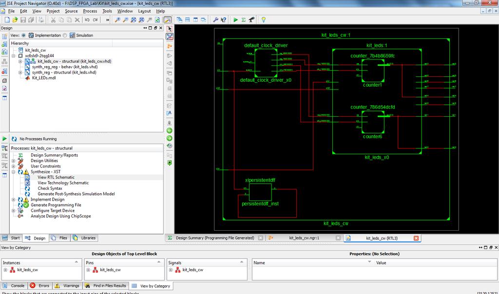
74 74 System Generator Tips Black Box: Let s you import any VHDL or Verilog file to your design


75 75 System Generator Tips Black Box: Once assigned the HDL file, input/outputs are automatically added Can be used to simulate HDL files
76 76 System Generator Example IO control Blinking some LEDs

77 77 System Generator Example Input pin

78 78 System Generator Example Output pin

79 79 System Generator Example Pulse on output

80 80 System Generator Example HDL Generation


81 81 System Generator Example HDL Generation

82 82 Use generated HDL HDL generation completed Next steps in ISE A project is built for ISE
83 83 ISE design suit Xilinx design suit for working with it s FPGAs Create project Synthesis Implement Generate programming file
84 84 ISE environment
85 85 Synthesis-Implement-Generate Programming File

86 86 View RTL Schematics

87 87 Programming the Device

88 88 Programming the Device

89 89 Programming the Device
90 90 System Generator Example PWM

91 91 System Generator Example Deadtime circuit for PWM
92 92 System Generator Example ADC interface for AD7822/5/9 2MSPS up to 8 channels
93 93 System Generator Example Channel selection for AD7822/5/9
94 94 Efficiency example
95 95 Design Example DSPbuilder for Altera FPGAs Example: Back to back three-phase converter

96 96 Design Example Overview of the control blocks Each subsystem contains some of control functionalities.
97 97 Design Example Example: implementation of Park conversion

98 98 Summary Section III Introduction to FPGA Matlab/Simulink for Model-based Design and Implementation of FPGAs Xilinx System Generator Review of Fixed-point Representation Overview of HDL Coder
99 99
100 100
101 101
102 102


103 103 Thanks for your attention!
Intro to System Generator. Objectives. After completing this module, you will be able to:
 Intro to System Generator This material exempt per Department of Commerce license exception TSU Objectives After completing this module, you will be able to: Explain why there is a need for an integrated
Basic Xilinx Design Capture. Objectives. After completing this module, you will be able to:
 Basic Xilinx Design Capture This material exempt per Department of Commerce license exception TSU Objectives After completing this module, you will be able to: List various blocksets available in System
SDR Spring KOMSYS-F6: Programmable Digital Devices (FPGAs)
") SDR Spring 2006 KOMSYS-F6: Programmable Digital Devices (FPGAs) Lecture 4 Jan Hvolgaard Mikkelsen Aalborg University 2006 Agenda What was the story about VHDL? o Quick recap from Lecture 3. Illustration
SDR Spring 2006 KOMSYS-F6: Programmable Digital Devices (FPGAs) Lecture 4 Jan Hvolgaard Mikkelsen Aalborg University 2006 Agenda What was the story about VHDL? o Quick recap from Lecture 3. Illustration
Method We follow- How to Get Entry Pass in SEMICODUCTOR Industries for 3rd year engineering. Winter/Summer Training
 Method We follow- How to Get Entry Pass in SEMICODUCTOR Industries for 3rd year engineering Winter/Summer Training Level 2 continues. 3 rd Year 4 th Year FIG-3 Level 1 (Basic & Mandatory) & Level 1.1 and
Agenda. Introduction FPGA DSP platforms Design challenges New programming models for FPGAs
 New Directions in Programming FPGAs for DSP Dr. Jim Hwang Xilinx, Inc. Agenda Introduction FPGA DSP platforms Design challenges New programming models for FPGAs System Generator Getting your math into
FPGA for Complex System Implementation. National Chiao Tung University Chun-Jen Tsai 04/14/2011
 FPGA for Complex System Implementation National Chiao Tung University Chun-Jen Tsai 04/14/2011 About FPGA FPGA was invented by Ross Freeman in 1989 SRAM-based FPGA properties Standard parts Allowing multi-level
Model-Based Design for effective HW/SW Co-Design Alexander Schreiber Senior Application Engineer MathWorks, Germany
 Model-Based Design for effective HW/SW Co-Design Alexander Schreiber Senior Application Engineer MathWorks, Germany 2013 The MathWorks, Inc. 1 Agenda Model-Based Design of embedded Systems Software Implementation
Optimize DSP Designs and Code using Fixed-Point Designer
 Optimize DSP Designs and Code using Fixed-Point Designer MathWorks Korea 이웅재부장 Senior Application Engineer 2013 The MathWorks, Inc. 1 Agenda Fixed-point concepts Introducing Fixed-Point Designer Overview
INTRODUCTION TO FPGA ARCHITECTURE
 3/3/25 INTRODUCTION TO FPGA ARCHITECTURE DIGITAL LOGIC DESIGN (BASIC TECHNIQUES) a b a y 2input Black Box y b Functional Schematic a b y a b y a b y 2 Truth Table (AND) Truth Table (OR) Truth Table (XOR)
Objectives. After completing this module, you will be able to:
 Signal Routing This material exempt per Department of Commerce license exception TSU Objectives After completing this module, you will be able to: Describe how signals are converted through Gateway In
A SIMULINK-TO-FPGA MULTI-RATE HIERARCHICAL FIR FILTER DESIGN
 A SIMULINK-TO-FPGA MULTI-RATE HIERARCHICAL FIR FILTER DESIGN Xiaoying Li 1 Fuming Sun 2 Enhua Wu 1, 3 1 University of Macau, Macao, China 2 University of Science and Technology Beijing, Beijing, China
FPGA: What? Why? Marco D. Santambrogio
 FPGA: What? Why? Marco D. Santambrogio marco.santambrogio@polimi.it 2 Reconfigurable Hardware Reconfigurable computing is intended to fill the gap between hardware and software, achieving potentially much
Implementing MATLAB Algorithms in FPGAs and ASICs By Alexander Schreiber Senior Application Engineer MathWorks
 Implementing MATLAB Algorithms in FPGAs and ASICs By Alexander Schreiber Senior Application Engineer MathWorks 2014 The MathWorks, Inc. 1 Traditional Implementation Workflow: Challenges Algorithm Development
Introduction to Field Programmable Gate Arrays
 Introduction to Field Programmable Gate Arrays Lecture 1/3 CERN Accelerator School on Digital Signal Processing Sigtuna, Sweden, 31 May 9 June 2007 Javier Serrano, CERN AB-CO-HT Outline Historical introduction.
OUTLINE RTL DESIGN WITH ARX
 1 2 RTL DESIGN WITH ARX IMPLEMENTATION OF DIGITAL SIGNAL PROCESSING Sabih H. Gerez University of Twente OUTLINE Design languages Arx motivation and alternatives Main features of Arx Arx language elements
Today. Comments about assignment Max 1/T (skew = 0) Max clock skew? Comments about assignment 3 ASICs and Programmable logic Others courses
 Max clock skew? Comments about assignment 3 ASICs and Programmable logic Others courses") Today Comments about assignment 3-43 Comments about assignment 3 ASICs and Programmable logic Others courses octor Per should show up in the end of the lecture Mealy machines can not be coded in a single
Today Comments about assignment 3-43 Comments about assignment 3 ASICs and Programmable logic Others courses octor Per should show up in the end of the lecture Mealy machines can not be coded in a single
FPGA introduction 2008
 FPGA introduction 2008 ecos is a registered trademark of ecoscentric Limited Øyvind Harboe, General Manager, Zylin AS What is an FPGA? Field Programmable Gate Array Not necessarily reprogrammable (anti-fuse,
FPGA Based Digital Design Using Verilog HDL
 FPGA Based Digital Design Using Course Designed by: IRFAN FAISAL MIR ( Verilog / FPGA Designer ) irfanfaisalmir@yahoo.com * Organized by Electronics Division Integrated Circuits Uses for digital IC technology
Signal Processing Algorithms into Fixed Point FPGA Hardware Dennis Silage ECE Temple University
 Signal Processing Algorithms into Fixed Point FPGA Hardware Dennis Silage silage@temple.edu ECE Temple University www.temple.edu/scdl Signal Processing Algorithms into Fixed Point FPGA Hardware Motivation
Modeling and implementation of dsp fpga solutions
 See discussions, stats, and author profiles for this publication at: https://www.researchgate.net/publication/228877179 Modeling and implementation of dsp fpga solutions Article CITATIONS 9 READS 57 4
Design and Verification of FPGA Applications
 Design and Verification of FPGA Applications Giuseppe Ridinò Paola Vallauri MathWorks giuseppe.ridino@mathworks.it paola.vallauri@mathworks.it Torino, 19 Maggio 2016, INAF 2016 The MathWorks, Inc. 1 Agenda
Field Programmable Gate Array (FPGA)
") Field Programmable Gate Array (FPGA) Lecturer: Krébesz, Tamas 1 FPGA in general Reprogrammable Si chip Invented in 1985 by Ross Freeman (Xilinx inc.) Combines the advantages of ASIC and uc-based systems
Field Programmable Gate Array (FPGA) Lecturer: Krébesz, Tamas 1 FPGA in general Reprogrammable Si chip Invented in 1985 by Ross Freeman (Xilinx inc.) Combines the advantages of ASIC and uc-based systems
Parallel FIR Filters. Chapter 5
 Chapter 5 Parallel FIR Filters This chapter describes the implementation of high-performance, parallel, full-precision FIR filters using the DSP48 slice in a Virtex-4 device. ecause the Virtex-4 architecture
Modeling a 4G LTE System in MATLAB
 Modeling a 4G LTE System in MATLAB Part 3: Path to implementation (C and HDL) Houman Zarrinkoub PhD. Signal Processing Product Manager MathWorks houmanz@mathworks.com 2011 The MathWorks, Inc. 1 LTE Downlink
EECS150 - Digital Design Lecture 6 - Field Programmable Gate Arrays (FPGAs)
") EECS150 - Digital Design Lecture 6 - Field Programmable Gate Arrays (FPGAs) September 12, 2002 John Wawrzynek Fall 2002 EECS150 - Lec06-FPGA Page 1 Outline What are FPGAs? Why use FPGAs (a short history
EECS150 - Digital Design Lecture 6 - Field Programmable Gate Arrays (FPGAs) September 12, 2002 John Wawrzynek Fall 2002 EECS150 - Lec06-FPGA Page 1 Outline What are FPGAs? Why use FPGAs (a short history
Xilinx System Generator v Xilinx Blockset Reference Guide. for Simulink. Introduction. Xilinx Blockset Overview.
 Xilinx System Generator v1.0.1 for Simulink Introduction Xilinx Blockset Overview Blockset Elements Xilinx Blockset Reference Guide Printed in U.S.A. Xilinx System Generator v1.0.1 Reference Guide About
Outline. EECS150 - Digital Design Lecture 6 - Field Programmable Gate Arrays (FPGAs) FPGA Overview. Why FPGAs?
 FPGA Overview. Why FPGAs?") EECS150 - Digital Design Lecture 6 - Field Programmable Gate Arrays (FPGAs) September 12, 2002 John Wawrzynek Outline What are FPGAs? Why use FPGAs (a short history lesson). FPGA variations Internal logic
EECS150 - Digital Design Lecture 6 - Field Programmable Gate Arrays (FPGAs) September 12, 2002 John Wawrzynek Outline What are FPGAs? Why use FPGAs (a short history lesson). FPGA variations Internal logic
Qsys and IP Core Integration
 Qsys and IP Core Integration Stephen A. Edwards (after David Lariviere) Columbia University Spring 2016 IP Cores Altera s IP Core Integration Tools Connecting IP Cores IP Cores Cyclone V SoC: A Mix of
Tutorial - Using Xilinx System Generator 14.6 for Co-Simulation on Digilent NEXYS3 (Spartan-6) Board
 Board") Tutorial - Using Xilinx System Generator 14.6 for Co-Simulation on Digilent NEXYS3 (Spartan-6) Board Shawki Areibi August 15, 2017 1 Introduction Xilinx System Generator provides a set of Simulink blocks
Tutorial - Using Xilinx System Generator 14.6 for Co-Simulation on Digilent NEXYS3 (Spartan-6) Board Shawki Areibi August 15, 2017 1 Introduction Xilinx System Generator provides a set of Simulink blocks
Model-Based Design for Video/Image Processing Applications
 Model-Based Design for Video/Image Processing Applications The MathWorks Agenda Model-Based Design From MATLAB and Simulink to Altera FPGA Step-by-step design and implementation of edge detection algorithm
FPGA Technology and Industry Experience
 FPGA Technology and Industry Experience Guest Lecture at HSLU, Horw (Lucerne) May 24 2012 Oliver Brndler, FPGA Design Center, Enclustra GmbH Silvio Ziegler, FPGA Design Center, Enclustra GmbH Content Enclustra
Objectives. Simulink Basics
 Simulink Basics This material exempt per Department of Commerce license exception TSU Objectives After completing this module, you will be able to: Describe Simulink environment List some of the commonly
Cover TBD. intel Quartus prime Design software
 Cover TBD intel Quartus prime Design software Fastest Path to Your Design The Intel Quartus Prime software is revolutionary in performance and productivity for FPGA, CPLD, and SoC designs, providing a
Hardware Design Environments. Dr. Mahdi Abbasi Computer Engineering Department Bu-Ali Sina University
 Hardware Design Environments Dr. Mahdi Abbasi Computer Engineering Department Bu-Ali Sina University Outline Welcome to COE 405 Digital System Design Design Domains and Levels of Abstractions Synthesis
Spiral 2-8. Cell Layout
 2-8.1 Spiral 2-8 Cell Layout 2-8.2 Learning Outcomes I understand how a digital circuit is composed of layers of materials forming transistors and wires I understand how each layer is expressed as geometric
Cover TBD. intel Quartus prime Design software
 Cover TBD intel Quartus prime Design software Fastest Path to Your Design The Intel Quartus Prime software is revolutionary in performance and productivity for FPGA, CPLD, and SoC designs, providing a
FPGA design with National Instuments
 FPGA design with National Instuments Rémi DA SILVA Systems Engineer - Embedded and Data Acquisition Systems - MED Region ni.com The NI Approach to Flexible Hardware Processor Real-time OS Application software
Design Methodologies. Full-Custom Design
 Design Methodologies Design styles Full-custom design Standard-cell design Programmable logic Gate arrays and field-programmable gate arrays (FPGAs) Sea of gates System-on-a-chip (embedded cores) Design
ibob ADC Tutorial CASPER Reference Design
 ibob ADC Tutorial Author: Griffin Foster April 14, 2009 (v1.0) Hardware Platforms Used: ibob, iadc FPGA Clock Rate: 100 MHz Sampling Rate: 400 MHz Software Environment: TinySH This tutorial walks through
Outline. EECS Components and Design Techniques for Digital Systems. Lec 11 Putting it all together Where are we now?
 Outline EECS 5 - Components and Design Techniques for Digital Systems Lec Putting it all together -5-4 David Culler Electrical Engineering and Computer Sciences University of California Berkeley Top-to-bottom
Digital Integrated Circuits
 Digital Integrated Circuits Lecture 9 Jaeyong Chung Robust Systems Laboratory Incheon National University DIGITAL DESIGN FLOW Chung EPC6055 2 FPGA vs. ASIC FPGA (A programmable Logic Device) Faster time-to-market
FPGA architecture and design technology
 CE 435 Embedded Systems Spring 2017 FPGA architecture and design technology Nikos Bellas Computer and Communications Engineering Department University of Thessaly 1 FPGA fabric A generic island-style FPGA
8. Best Practices for Incremental Compilation Partitions and Floorplan Assignments
 8. Best Practices for Incremental Compilation Partitions and Floorplan Assignments QII51017-9.0.0 Introduction The Quartus II incremental compilation feature allows you to partition a design, compile partitions
Accelerating FPGA/ASIC Design and Verification
 Accelerating FPGA/ASIC Design and Verification Tabrez Khan Senior Application Engineer Vidya Viswanathan Application Engineer 2015 The MathWorks, Inc. 1 Agenda Challeges with Traditional Implementation
The Xilinx XC6200 chip, the software tools and the board development tools
 The Xilinx XC6200 chip, the software tools and the board development tools What is an FPGA? Field Programmable Gate Array Fully programmable alternative to a customized chip Used to implement functions
Real-Time Testing in a Modern, Agile Development Workflow
 Real-Time Testing in a Modern, Agile Development Workflow Simon Eriksson Application Engineer 2015 The MathWorks, Inc. 1 Demo Going from Desktop Testing to Real-Time Testing 2 Key Take-Aways From This
Design Methodologies and Tools. Full-Custom Design
 Design Methodologies and Tools Design styles Full-custom design Standard-cell design Programmable logic Gate arrays and field-programmable gate arrays (FPGAs) Sea of gates System-on-a-chip (embedded cores)
FPGA for Software Engineers
 FPGA for Software Engineers Course Description This course closes the gap between hardware and software engineers by providing the software engineer all the necessary FPGA concepts and terms. The course
Design and Verification of FPGA and ASIC Applications Graham Reith MathWorks
 Design and Verification of FPGA and ASIC Applications Graham Reith MathWorks 2014 The MathWorks, Inc. 1 Agenda -Based Design for FPGA and ASIC Generating HDL Code from MATLAB and Simulink For prototyping
FPGAs: FAST TRACK TO DSP
 FPGAs: FAST TRACK TO DSP Revised February 2009 ABSRACT: Given the prevalence of digital signal processing in a variety of industry segments, several implementation solutions are available depending on
Topics. Midterm Finish Chapter 7
 Lecture 9 Topics Midterm Finish Chapter 7 ROM (review) Memory device in which permanent binary information is stored. Example: 32 x 8 ROM Five input lines (2 5 = 32) 32 outputs, each representing a memory
Hardware Design with VHDL PLDs IV ECE 443
 Embedded Processor Cores (Hard and Soft) Electronic design can be realized in hardware (logic gates/registers) or software (instructions executed on a microprocessor). The trade-off is determined by how
Programmable Logic Devices
 Programmable Logic Devices INTRODUCTION A programmable logic device or PLD is an electronic component used to build reconfigurable digital circuits. Unlike a logic gate, which has a fixed function, a PLD
Evolution of CAD Tools & Verilog HDL Definition
 Evolution of CAD Tools & Verilog HDL Definition K.Sivasankaran Assistant Professor (Senior) VLSI Division School of Electronics Engineering VIT University Outline Evolution of CAD Different CAD Tools for
Experiment 3. Digital Circuit Prototyping Using FPGAs
 Experiment 3. Digital Circuit Prototyping Using FPGAs Masud ul Hasan Muhammad Elrabaa Ahmad Khayyat Version 151, 11 September 2015 Table of Contents 1. Objectives 2. Materials Required 3. Background 3.1.
Vivado Design Suite Tutorial. Model-Based DSP Design using System Generator
 Vivado Design Suite Tutorial Model-Based DSP Design using System Generator Notice of Disclaimer The information disclosed to you hereunder (the "Materials") is provided solely for the selection and use
RTL Coding General Concepts
 RTL Coding General Concepts Typical Digital System 2 Components of a Digital System Printed circuit board (PCB) Embedded d software microprocessor microcontroller digital signal processor (DSP) ASIC Programmable
The QR code here provides a shortcut to go to the course webpage.
 Welcome to this MSc Lab Experiment. All my teaching materials for this Lab-based module are also available on the webpage: www.ee.ic.ac.uk/pcheung/teaching/msc_experiment/ The QR code here provides a shortcut
A Matlab/Simulink Simulation Approach for Early Field-Programmable Gate Array Hardware Evaluation
 A Matlab/Simulink Simulation Approach for Early Field-Programmable Gate Array Hardware Evaluation Celso Coslop Barbante, José Raimundo de Oliveira Computing Laboratory (COMLAB) Department of Computer Engineering
Hardware Implementation and Verification by Model-Based Design Workflow - Communication Models to FPGA-based Radio
 Hardware Implementation and Verification by -Based Design Workflow - Communication s to FPGA-based Radio Katsuhisa Shibata Industry Marketing MathWorks Japan 2015 The MathWorks, Inc. 1 Agenda Challenges
Connecting MATLAB & Simulink with your SystemVerilog Workflow for Functional Verification
 Connecting MATLAB & Simulink with your SystemVerilog Workflow for Functional Verification Corey Mathis Industry Marketing Manager Communications, Electronics, and Semiconductors MathWorks 2014 MathWorks,
Reducing the cost of FPGA/ASIC Verification with MATLAB and Simulink
 Reducing the cost of FPGA/ASIC Verification with MATLAB and Simulink Graham Reith Industry Manager Communications, Electronics and Semiconductors MathWorks Graham.Reith@mathworks.co.uk 2015 The MathWorks,
COMPARISON OF DIFFERENT REALIZATION TECHNIQUES OF IIR FILTERS USING SYSTEM GENERATOR
 COMPARISON OF DIFFERENT REALIZATION TECHNIQUES OF IIR FILTERS USING SYSTEM GENERATOR Prof. SunayanaPatil* Pratik Pramod Bari**, VivekAnandSakla***, Rohit Ashok Shah****, DharmilAshwin Shah***** *(sunayana@vcet.edu.in)
Simulink Design Environment
 EE219A Spring 2008 Special Topics in Circuits and Signal Processing Lecture 4 Simulink Design Environment Dejan Markovic dejan@ee.ucla.edu Announcements Class wiki Material being constantly updated Please
Digital Design Methodology (Revisited) Design Methodology: Big Picture
 Design Methodology: Big Picture") Digital Design Methodology (Revisited) Design Methodology Design Specification Verification Synthesis Technology Options Full Custom VLSI Standard Cell ASIC FPGA CS 150 Fall 2005 - Lec #25 Design Methodology
Digital Design Methodology (Revisited) Design Methodology Design Specification Verification Synthesis Technology Options Full Custom VLSI Standard Cell ASIC FPGA CS 150 Fall 2005 - Lec #25 Design Methodology
Design Methodologies
 Design Methodologies 1981 1983 1985 1987 1989 1991 1993 1995 1997 1999 2001 2003 2005 2007 2009 Complexity Productivity (K) Trans./Staff - Mo. Productivity Trends Logic Transistor per Chip (M) 10,000 0.1
Digital Design Methodology
 Digital Design Methodology Prof. Soo-Ik Chae Digital System Designs and Practices Using Verilog HDL and FPGAs @ 2008, John Wiley 1-1 Digital Design Methodology (Added) Design Methodology Design Specification
Introduction to. DSP Using FPGAs. Guillermo Güichal UTN FRBB
 Introduction to DSP Using FPGAs Guillermo Güichal UTN FRBB Program Morning Introduction to DSP What is DSP? How is it done? Why use FPGAs for DSP? Comments on DSP algorithms and FPGA implementations. Issues
FPGA Design Flow 1. All About FPGA
 FPGA Design Flow 1 In this part of tutorial we are going to have a short intro on FPGA design flow. A simplified version of FPGA design flow is given in the flowing diagram. FPGA Design Flow 2 FPGA_Design_FLOW
FPGA. Logic Block. Plessey FPGA: basic building block here is 2-input NAND gate which is connected to each other to implement desired function.
 FPGA Logic block of an FPGA can be configured in such a way that it can provide functionality as simple as that of transistor or as complex as that of a microprocessor. It can used to implement different
Overview. CSE372 Digital Systems Organization and Design Lab. Hardware CAD. Two Types of Chips
 Overview CSE372 Digital Systems Organization and Design Lab Prof. Milo Martin Unit 5: Hardware Synthesis CAD (Computer Aided Design) Use computers to design computers Virtuous cycle Architectural-level,
TSEA44 - Design for FPGAs
 2015-11-24 Now for something else... Adapting designs to FPGAs Why? Clock frequency Area Power Target FPGA architecture: Xilinx FPGAs with 4 input LUTs (such as Virtex-II) Determining the maximum frequency
I 3 I 2. ! Language of logic design " Logic optimization, state, timing, CAD tools
 Course Wrap-up Let s Try the Priority Encoder One More Time = =! Priority Encoder Revisited! What (We Hope) You Learned I 3 O 3 I j O j! Design Methodology! I 2 O 2 I O I O Zero Oj Ij Ij CS 5 - Spring
Topics. Midterm Finish Chapter 7
 Lecture 9 Topics Midterm Finish Chapter 7 Xilinx FPGAs Chapter 7 Spartan 3E Architecture Source: Spartan-3E FPGA Family Datasheet CLB Configurable Logic Blocks Each CLB contains four slices Each slice
CMPE 415 Programmable Logic Devices Introduction
 Department of Computer Science and Electrical Engineering CMPE 415 Programmable Logic Devices Introduction Prof. Ryan Robucci What are FPGAs? Field programmable Gate Array Typically re programmable as
Digital Logic & Computer Design CS Professor Dan Moldovan Spring 2010
 Digital Logic & Computer Design CS 434 Professor Dan Moldovan Spring 2 Copyright 27 Elsevier 5- Chapter 5 :: Digital Building Blocks Digital Design and Computer Architecture David Money Harris and Sarah
LSN 6 Programmable Logic Devices
 LSN 6 Programmable Logic Devices Department of Engineering Technology LSN 6 What Are PLDs? Functionless devices in base form Require programming to operate The logic function of the device is programmed
What is Xilinx Design Language?
 Bill Jason P. Tomas University of Nevada Las Vegas Dept. of Electrical and Computer Engineering What is Xilinx Design Language? XDL is a human readable ASCII format compatible with the more widely used
An Introduction to Programmable Logic
 Outline An Introduction to Programmable Logic 3 November 24 Transistors Logic Gates CPLD Architectures FPGA Architectures Device Considerations Soft Core Processors Design Example Quiz Semiconductors Semiconductor
: : (91-44) (Office) (91-44) (Residence)
 (Office) (91-44) (Residence)") Course: VLSI Circuits (Video Course) Faculty Coordinator(s) : Prof. S. Srinivasan Department of Electrical Engineering Indian Institute of Technology Madras Chennai 600036 Email Telephone : srinis@iitm.ac.in,
Course: VLSI Circuits (Video Course) Faculty Coordinator(s) : Prof. S. Srinivasan Department of Electrical Engineering Indian Institute of Technology Madras Chennai 600036 Email Telephone : srinis@iitm.ac.in,
PLAs & PALs. Programmable Logic Devices (PLDs) PLAs and PALs
 PLAs and PALs") PLAs & PALs Programmable Logic Devices (PLDs) PLAs and PALs PLAs&PALs By the late 1970s, standard logic devices were all the rage, and printed circuit boards were loaded with them. To offer the ultimate
PLAs & PALs Programmable Logic Devices (PLDs) PLAs and PALs PLAs&PALs By the late 1970s, standard logic devices were all the rage, and printed circuit boards were loaded with them. To offer the ultimate
Very Large Scale Integration (VLSI)
") Very Large Scale Integration (VLSI) Lecture 6 Dr. Ahmed H. Madian Ah_madian@hotmail.com Dr. Ahmed H. Madian-VLSI 1 Contents FPGA Technology Programmable logic Cell (PLC) Mux-based cells Look up table PLA
Very Large Scale Integration (VLSI) Lecture 6 Dr. Ahmed H. Madian Ah_madian@hotmail.com Dr. Ahmed H. Madian-VLSI 1 Contents FPGA Technology Programmable logic Cell (PLC) Mux-based cells Look up table PLA
ISE Design Suite Software Manuals and Help
 ISE Design Suite Software Manuals and Help These documents support the Xilinx ISE Design Suite. Click a document title on the left to view a document, or click a design step in the following figure to
MATLAB/Simulink 기반의프로그래머블 SoC 설계및검증
 MATLAB/Simulink 기반의프로그래머블 SoC 설계및검증 이웅재부장 Application Engineering Group 2014 The MathWorks, Inc. 1 Agenda Introduction ZYNQ Design Process Model-Based Design Workflow Prototyping and Verification Processor
Digital Electronics 27. Digital System Design using PLDs
 1 Module -27 Digital System Design 1. Introduction 2. Digital System Design 2.1 Standard (Fixed function) ICs based approach 2.2 Programmable ICs based approach 3. Comparison of Digital System Design approaches
CHAPTER-IV IMPLEMENTATION AND ANALYSIS OF FPGA-BASED DESIGN OF 32-BIT FPAU
 CHAPTER-IV IMPLEMENTATION AND ANALYSIS OF FPGA-BASED DESIGN OF 32-BIT FPAU The design of 32 bit FPAU using VHDL presented in chapter III needs to be further implemented and tested on FPGA platform and
Design Guidelines for Optimal Results in High-Density FPGAs
 White Paper Introduction Design Guidelines for Optimal Results in High-Density FPGAs Today s FPGA applications are approaching the complexity and performance requirements of ASICs. In some cases, FPGAs
Best Practices for Incremental Compilation Partitions and Floorplan Assignments
 Best Practices for Incremental Compilation Partitions and Floorplan Assignments December 2007, ver. 1.0 Application Note 470 Introduction The Quartus II incremental compilation feature allows you to partition
DSP Builder User Guide
 DSP Builder User Guide 101 Innovation Drive San Jose, CA 95134 www.altera.com Software Version: 7.2 SP1 Document Date: December 2007 Copyright 2007 Altera Corporation. All rights reserved. Altera, The
DSP Builder Handbook Volume 1: Introduction to DSP Builder
 DSP Builder Handbook Volume 1: Introduction to DSP Builder DSP Builder Handbook 101 Innovation Drive San Jose, CA 95134 www.altera.com HB_DSPB_INTRO-5.1 Document last updated for Altera Complete Design
COE 561 Digital System Design & Synthesis Introduction
 1 COE 561 Digital System Design & Synthesis Introduction Dr. Aiman H. El-Maleh Computer Engineering Department King Fahd University of Petroleum & Minerals Outline Course Topics Microelectronics Design
Evolution of Implementation Technologies. ECE 4211/5211 Rapid Prototyping with FPGAs. Gate Array Technology (IBM s) Programmable Logic
 Programmable Logic") ECE 42/52 Rapid Prototyping with FPGAs Dr. Charlie Wang Department of Electrical and Computer Engineering University of Colorado at Colorado Springs Evolution of Implementation Technologies Discrete devices:
ECE 42/52 Rapid Prototyping with FPGAs Dr. Charlie Wang Department of Electrical and Computer Engineering University of Colorado at Colorado Springs Evolution of Implementation Technologies Discrete devices:
System-on Solution from Altera and Xilinx
 System-on on-a-programmable-chip Solution from Altera and Xilinx Xun Yang VLSI CAD Lab, Computer Science Department, UCLA FPGAs with Embedded Microprocessors Combination of embedded processors and programmable
EE 4755 Digital Design Using Hardware Description Languages
 EE 4755 Digital Design Using Hardware Description Languages Basic Information URL: http://www.ece.lsu.edu/v Offered by: David M. Koppelman, Room 345 ERAD Building 578-5482. koppel@ece.lsu.edu, http://www.ece.lsu.edu/koppel/koppel.html
Verilog for High Performance
 Verilog for High Performance Course Description This course provides all necessary theoretical and practical know-how to write synthesizable HDL code through Verilog standard language. The course goes
INTRODUCTION TO FIELD PROGRAMMABLE GATE ARRAYS (FPGAS)
") INTRODUCTION TO FIELD PROGRAMMABLE GATE ARRAYS (FPGAS) Bill Jason P. Tomas Dept. of Electrical and Computer Engineering University of Nevada Las Vegas FIELD PROGRAMMABLE ARRAYS Dominant digital design
INTRODUCTION TO FIELD PROGRAMMABLE GATE ARRAYS (FPGAS) Bill Jason P. Tomas Dept. of Electrical and Computer Engineering University of Nevada Las Vegas FIELD PROGRAMMABLE ARRAYS Dominant digital design
Choosing an Intellectual Property Core
 Choosing an Intellectual Property Core MIPS Technologies, Inc. June 2002 One of the most important product development decisions facing SOC designers today is choosing an intellectual property (IP) core.
[Sub Track 1-3] FPGA/ASIC 을타겟으로한알고리즘의효율적인생성방법및신기능소개
![[Sub Track 1-3] FPGA/ASIC 을타겟으로한알고리즘의효율적인생성방법및신기능소개](/thumbs/82/85868302.jpg "[Sub Track 1-3] FPGA/ASIC 을타겟으로한알고리즘의효율적인생성방법및신기능소개") [Sub Track 1-3] FPGA/ASIC 을타겟으로한알고리즘의효율적인생성방법및신기능소개 정승혁과장 Senior Application Engineer MathWorks Korea 2015 The MathWorks, Inc. 1 Outline When FPGA, ASIC, or System-on-Chip (SoC) hardware is needed Hardware
[Sub Track 1-3] FPGA/ASIC 을타겟으로한알고리즘의효율적인생성방법및신기능소개 정승혁과장 Senior Application Engineer MathWorks Korea 2015 The MathWorks, Inc. 1 Outline When FPGA, ASIC, or System-on-Chip (SoC) hardware is needed Hardware
Wordlength Optimization
 EE216B: VLSI Signal Processing Wordlength Optimization Prof. Dejan Marković ee216b@gmail.com Number Systems: Algebraic Algebraic Number e.g. a = + b [1] High level abstraction Infinite precision Often
101-1 Under-Graduate Project Digital IC Design Flow
 101-1 Under-Graduate Project Digital IC Design Flow Speaker: Ming-Chun Hsiao Adviser: Prof. An-Yeu Wu Date: 2012/9/25 ACCESS IC LAB Outline Introduction to Integrated Circuit IC Design Flow Verilog HDL