Design Methodologies
|
|
|
- Jasper Robbins
- 5 years ago
- Views:
Transcription

1 Design Methodologies
2 Complexity Productivity (K) Trans./Staff - Mo. Productivity Trends Logic Transistor per Chip (M) 10, mm 1, mm mm Logic Tr./Chip Tr./Staff Month. x x x x x x x x 58%/Yr. compounded Complexity growth rate 21%/Yr. compound Productivity growth rate 100, ,000,000 10,000 10,000,000 1,000 1,000, , , , Source: Sematech Complexity outpaces design productivity 2
3 INPUT/OUTPUT A Simple Processor MEMORY CONTROL INPUT-OUTPUT DATAPATH 3

4 A System-on-a-Chip: Example 4
 5")
5 Energy Efficiency (in MOPS/mW) Hardwired custom Configurable/Parameterizable Domain-specific processor (e.g. DSP) Embedded microprocessor Impact of Implementation Choices None Somewhat flexible Fully flexible Flexibility (or application scope) 5
6 Implementation Choices Digital Circuit Implementation Approaches Custom Semicustom Cell-based Array-based Standard Cells Compiled Cells Macro Cells Pre-diffused (Gate Arrays) Pre-wired (FPGA's) 6

7 The Custom Approach Intel


")

8 Transition to Automation and Regular Structures Intel 4004 ( 71) Intel 8080 Intel 8085 Intel 8286 Intel


9 Cell-based Design Routing channel requirements are reduced by presence of more interconnect layers Standard Cell Layout methodology 9

10 The Evolution of Standard Cell [Brodersen92] 10

11 Standard Cell The New Generation Cell-structure hidden under interconnect layers 11

12 Standard Cell - Example 3-input NAND cell (from ST Microelectronics): 12


13 Automatic Cell Generation Initial transistor geometries Placed transistors Routed cell Compacted cell Finished cell 13

14 MacroModules (or 8192 bit) SRAM Generated by hard-macro module generator Implemented in 0.18 mm CMOS technology (0.094 mm 2 ) 14


15 Soft MacroModules 8 x 8 Multiplier Synopsys DesignCompiler 15


16 Design Iteration Semicustom Design Flow Pre-Layout Simulation Design Capture HDL Logic Synthesis Behavioral Structural Post-Layout Simulation Circuit Extraction Floorplanning Placement Routing Physical Tape-out 16


17 The Design Closure Problem Iterative Removal of Timing Violations (white lines) Courtesy Synopsys 17

18 Integrating Synthesis with Physical Design RTL (Timing) Constraints Physical Synthesis Macromodules Fixed netlists Netlist with Place-and-Route Info Place-and-Route Optimization Artwork 18
19 Late-Binding Implementation Array-based Pre-diffused (Gate Arrays) Pre-wired (FPGA's) 19
20 Gate Array Sea-of-gates polysilicon In1 In2 In3 In4 V DD metal GND possible contact Out Uncommited Cell Committed Cell (4-input NOR) 20

21 Gate Array Architectures 21
22 Examples of Sea-of-gate Primitive Cells Oxide-isolation PMOS PMOS NMOS NMOS NMOS Using oxide-isolation Using gate-isolation 22

23 Sea-of-gates Random Logic Memory Subsystem LSI Logic LEA300K (0.6 mm CMOS) 23
24 Xilinx FPGA Architecture 24
25 Antifuse-Based FPGA antifuse polysilicon ONO dielectric n + antifuse diffusion 2 l Open by default, closed by applying current pulse 25

26 RAM-based FPGA Xilinx XC4000ex 26
27 Two-Level Logic Every logic function can be expressed in sumof-products format (AND-OR) x 0 x 1 Product terms Inverting format (NOR-NOR) more effective AND plane x 2 OR plane f 0 f 1 x 0 x 1 x 2 27
28 Array-Based Programmable Logic (1) I 3 I 2 I 1 I 0 Programmable OR array Fixed AND array PROM O 3 O 2 O 1 O 0 Indicates programmable connection Indicates fixed connection 28
29 Programming a PROM 1 X 2 X 1 X 0 : programmed node NA NA f 1 f 0 29
30 Array-Based Programmable Logic (2) I 5 I 4 I 3 I 2 I 1 I 0 Programmable OR array Programmable AND array PLA O 1 O 2 O 3 O 0 30
31 Array-Based Programmable Logic (3) I 5 I 4 I 3 I 2 I 1 I 0 Fixed OR array Programmable AND array PAL O 1 O 2 O 3 O 0 Indicates programmable connection Indicates fixed connection 31

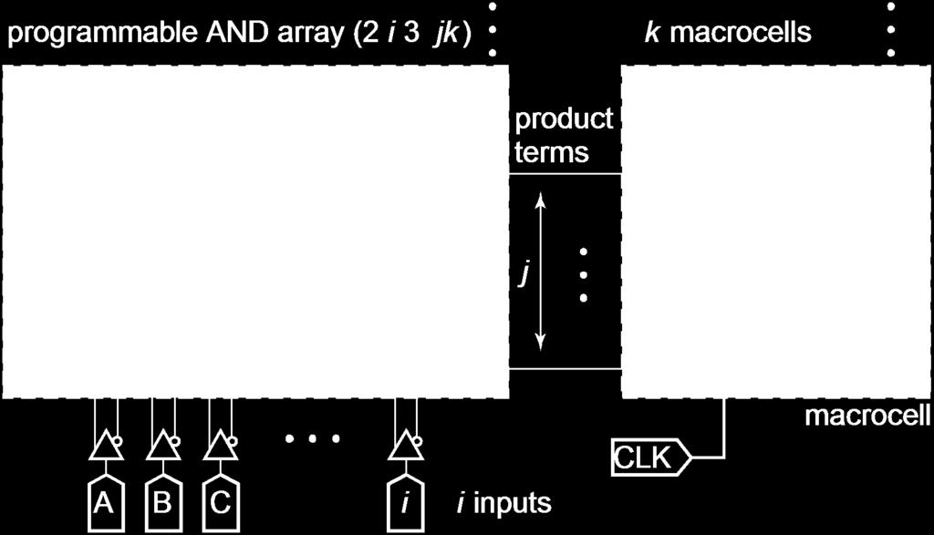
32 More Complex PAL i x i inputs, j minterms/macrocell, k macrocells 32

33 PLA Layout Exploiting Regularity V DD And-Plane Or-Plane f GND x 0 x 0 x 1 x 1 x 2 x 2 Pull-up devices f 0 f 1 Pull-up devices 33
34 Cell-Based Programmable Logic A 0 B 1 S 2-input mux as programmable logic block F Configuration A B S F= X 1 X 0 Y 1 Y 0 Y X XY X 0 Y XY Y 0 X XY Y 1 X X + Y 1 0 X X 1 0 Y Y F = A S + B S 34
35 Logic Cell of Actel Fuse-Based FPGA A B 1 SA C 1 Y D 1 SB S0 S1 35
36 Memory Look-up Table Based Logic Cell In Out Out ln1 ln2 Cell schematic XOR function 36
37 LUT-Based Logic Cell Xilinx 4000 Series 37

38 Array-Based Programmable Wiring M Interconnect Point Programmed interconnection Input/output pin Cell Horizontal tracks Vertical tracks 38
39 Mesh-based Interconnect Network Switch Box Connect Box Interconnect Point 39
40 Transistor Implementation of Mesh 40

41 Hierarchical Mesh Network Use overlayed mesh to support longer connections Reduced fanout and reduced resistance 41
42 Prewired Arrays Classification of prewired arrays (or fieldprogrammable devices): Based on Programming Technique Fuse-based (program-once) Non-volatile EPROM based RAM based Programmable Logic Style Array-Based Look-up Table Programmable Interconnect Style Channel-routing Mesh networks 42
43 Analog System-on-a-Chip Multi- Spectral RAM Imager 500 k Gates FPGA + 1 Gbit DRAM Preprocessing 64 SIMD Processor Array + SRAM Image Conditioning 100 GOPS mc system +2 Gbit DRAM Recognition Embedded applications where cost, performance, and energy are the real issues! DSP and control intensive Mixed-mode Combines programmable and application-specific modules Software plays crucial role 43

44 Heterogeneous Programmable Platforms FPGA Fabric Embedded PowerPc Embedded memories Hardwired multipliers High-speed I/O Xilinx Vertex-II Pro 44

45 Berkeley Pleiades Processor Interface FPGA Reconfigurable Data-path ARM8 Core 0.25um 6-level metal CMOS 5.2mm x 6.7mm 1.2 Million transistors 40 MHz at 1V 2 extra supplies: 0.4V, 1.5V 1.5~2 mw power dissipation 45
46 Summary Digital CMOS Design is kicking and healthy Some major challenges down the road caused by Deep Sub-micron Super GHz design Power consumption!!!! Reliability making it work Some new circuit solutions are bound to emerge Who can afford design in the years to come? Some major design methodology change in the making! 46
Design Methodologies. Digital Integrated Circuits A Design Perspective. Jan M. Rabaey Anantha Chandrakasan Borivoje Nikolic.
 Digital Integrated Circuits A Design Perspective Jan M. Rabaey Anantha Chandrakasan Borivoje Nikolic Design Methodologies December 10, 2002 L o g i c T r a n s i s t o r s p e r C h i p ( K ) 1 9 8 1 1
EE 466/586 VLSI Design. Partha Pande School of EECS Washington State University
 EE 466/586 VLSI Design Partha Pande School of EECS Washington State University pande@eecs.wsu.edu Lecture 18 Implementation Methods The Design Productivity Challenge Logic Transistors per Chip (K) 10,000,000.10m
FYSE420 DIGITAL ELECTRONICS. Lecture 7
 FYSE420 DIGITAL ELECTRONICS Lecture 7 1 [1] [2] [3] DIGITAL LOGIC CIRCUIT ANALYSIS & DESIGN Nelson, Nagle, Irvin, Carrol ISBN 0-13-463894-8 DIGITAL DESIGN Morris Mano Fourth edition ISBN 0-13-198924-3
PROGRAMMABLE MODULES SPECIFICATION OF PROGRAMMABLE COMBINATIONAL AND SEQUENTIAL MODULES
 PROGRAMMABLE MODULES SPECIFICATION OF PROGRAMMABLE COMBINATIONAL AND SEQUENTIAL MODULES. psa. rom. fpga THE WAY THE MODULES ARE PROGRAMMED NETWORKS OF PROGRAMMABLE MODULES EXAMPLES OF USES Programmable
Announcements. Midterm 2 next Thursday, 6-7:30pm, 277 Cory Review session on Tuesday, 6-7:30pm, 277 Cory Homework 8 due next Tuesday Labs: project
 - Fall 2002 Lecture 20 Synthesis Sequential Logic Announcements Midterm 2 next Thursday, 6-7:30pm, 277 Cory Review session on Tuesday, 6-7:30pm, 277 Cory Homework 8 due next Tuesday Labs: project» Teams
Design Methodologies and Tools. Full-Custom Design
 Design Methodologies and Tools Design styles Full-custom design Standard-cell design Programmable logic Gate arrays and field-programmable gate arrays (FPGAs) Sea of gates System-on-a-chip (embedded cores)
Spiral 2-8. Cell Layout
 2-8.1 Spiral 2-8 Cell Layout 2-8.2 Learning Outcomes I understand how a digital circuit is composed of layers of materials forming transistors and wires I understand how each layer is expressed as geometric
Design Methodologies. Full-Custom Design
 Design Methodologies Design styles Full-custom design Standard-cell design Programmable logic Gate arrays and field-programmable gate arrays (FPGAs) Sea of gates System-on-a-chip (embedded cores) Design
Overview. CSE372 Digital Systems Organization and Design Lab. Hardware CAD. Two Types of Chips
 Overview CSE372 Digital Systems Organization and Design Lab Prof. Milo Martin Unit 5: Hardware Synthesis CAD (Computer Aided Design) Use computers to design computers Virtuous cycle Architectural-level,
PLAs & PALs. Programmable Logic Devices (PLDs) PLAs and PALs
 PLAs and PALs") PLAs & PALs Programmable Logic Devices (PLDs) PLAs and PALs PLAs&PALs By the late 1970s, standard logic devices were all the rage, and printed circuit boards were loaded with them. To offer the ultimate
PLAs & PALs Programmable Logic Devices (PLDs) PLAs and PALs PLAs&PALs By the late 1970s, standard logic devices were all the rage, and printed circuit boards were loaded with them. To offer the ultimate
FABRICATION TECHNOLOGIES
 FABRICATION TECHNOLOGIES DSP Processor Design Approaches Full custom Standard cell** higher performance lower energy (power) lower per-part cost Gate array* FPGA* Programmable DSP Programmable general
CAD for VLSI. Debdeep Mukhopadhyay IIT Madras
 CAD for VLSI Debdeep Mukhopadhyay IIT Madras Tentative Syllabus Overall perspective of VLSI Design MOS switch and CMOS, MOS based logic design, the CMOS logic styles, Pass Transistors Introduction to Verilog
FPGA for Complex System Implementation. National Chiao Tung University Chun-Jen Tsai 04/14/2011
 FPGA for Complex System Implementation National Chiao Tung University Chun-Jen Tsai 04/14/2011 About FPGA FPGA was invented by Ross Freeman in 1989 SRAM-based FPGA properties Standard parts Allowing multi-level
CS310 Embedded Computer Systems. Maeng
 1 INTRODUCTION (PART II) Maeng Three key embedded system technologies 2 Technology A manner of accomplishing a task, especially using technical processes, methods, or knowledge Three key technologies for
EE586 VLSI Design. Partha Pande School of EECS Washington State University
 EE586 VLSI Design Partha Pande School of EECS Washington State University pande@eecs.wsu.edu Lecture 1 (Introduction) Why is designing digital ICs different today than it was before? Will it change in
Lab. Course Goals. Topics. What is VLSI design? What is an integrated circuit? VLSI Design Cycle. VLSI Design Automation
 Course Goals Lab Understand key components in VLSI designs Become familiar with design tools (Cadence) Understand design flows Understand behavioral, structural, and physical specifications Be able to
ECE 636. Reconfigurable Computing. Lecture 2. Field Programmable Gate Arrays I
 ECE 636 Reconfigurable Computing Lecture 2 Field Programmable Gate Arrays I Overview Anti-fuse and EEPROM-based devices Contemporary SRAM devices - Wiring - Embedded New trends - Single-driver wiring -
DIGITAL DESIGN TECHNOLOGY & TECHNIQUES
 DIGITAL DESIGN TECHNOLOGY & TECHNIQUES CAD for ASIC Design 1 INTEGRATED CIRCUITS (IC) An integrated circuit (IC) consists complex electronic circuitries and their interconnections. William Shockley et
Memory and Programmable Logic
 Digital Circuit Design and Language Memory and Programmable Logic Chang, Ik Joon Kyunghee University Memory Classification based on functionality ROM : Read-Only Memory RWM : Read-Write Memory RWM NVRWM
VLSI Design Automation
 VLSI Design Automation IC Products Processors CPU, DSP, Controllers Memory chips RAM, ROM, EEPROM Analog Mobile communication, audio/video processing Programmable PLA, FPGA Embedded systems Used in cars,
Chapter 5: ASICs Vs. PLDs
 Chapter 5: ASICs Vs. PLDs 5.1 Introduction A general definition of the term Application Specific Integrated Circuit (ASIC) is virtually every type of chip that is designed to perform a dedicated task.
VLSI Design Automation
 VLSI Design Automation IC Products Processors CPU, DSP, Controllers Memory chips RAM, ROM, EEPROM Analog Mobile communication, audio/video processing Programmable PLA, FPGA Embedded systems Used in cars,
VLSI Design Automation. Maurizio Palesi
 VLSI Design Automation 1 Outline Technology trends VLSI Design flow (an overview) 2 Outline Technology trends VLSI Design flow (an overview) 3 IC Products Processors CPU, DSP, Controllers Memory chips
An Introduction to Programmable Logic
 Outline An Introduction to Programmable Logic 3 November 24 Transistors Logic Gates CPLD Architectures FPGA Architectures Device Considerations Soft Core Processors Design Example Quiz Semiconductors Semiconductor
LSN 6 Programmable Logic Devices
 LSN 6 Programmable Logic Devices Department of Engineering Technology LSN 6 What Are PLDs? Functionless devices in base form Require programming to operate The logic function of the device is programmed
CHAPTER 12 ARRAY SUBSYSTEMS [ ] MANJARI S. KULKARNI
![CHAPTER 12 ARRAY SUBSYSTEMS [ ] MANJARI S. KULKARNI](/thumbs/76/73997056.jpg "CHAPTER 12 ARRAY SUBSYSTEMS [ ] MANJARI S. KULKARNI") CHAPTER 2 ARRAY SUBSYSTEMS [2.4-2.9] MANJARI S. KULKARNI OVERVIEW Array classification Non volatile memory Design and Layout Read-Only Memory (ROM) Pseudo nmos and NAND ROMs Programmable ROMS PROMS, EPROMs,
CHAPTER 2 ARRAY SUBSYSTEMS [2.4-2.9] MANJARI S. KULKARNI OVERVIEW Array classification Non volatile memory Design and Layout Read-Only Memory (ROM) Pseudo nmos and NAND ROMs Programmable ROMS PROMS, EPROMs,
VLSI Design Automation. Calcolatori Elettronici Ing. Informatica
 VLSI Design Automation 1 Outline Technology trends VLSI Design flow (an overview) 2 IC Products Processors CPU, DSP, Controllers Memory chips RAM, ROM, EEPROM Analog Mobile communication, audio/video processing
ECE 459/559 Secure & Trustworthy Computer Hardware Design
 ECE 459/559 Secure & Trustworthy Computer Hardware Design VLSI Design Basics Garrett S. Rose Spring 2016 Recap Brief overview of VHDL Behavioral VHDL Structural VHDL Simple examples with VHDL Some VHDL
Very Large Scale Integration (VLSI)
") Very Large Scale Integration (VLSI) Lecture 6 Dr. Ahmed H. Madian Ah_madian@hotmail.com Dr. Ahmed H. Madian-VLSI 1 Contents FPGA Technology Programmable logic Cell (PLC) Mux-based cells Look up table PLA
Very Large Scale Integration (VLSI) Lecture 6 Dr. Ahmed H. Madian Ah_madian@hotmail.com Dr. Ahmed H. Madian-VLSI 1 Contents FPGA Technology Programmable logic Cell (PLC) Mux-based cells Look up table PLA
EE241 - Spring 2004 Advanced Digital Integrated Circuits
 EE24 - Spring 2004 Advanced Digital Integrated Circuits Borivoje Nikolić Lecture 2 Impact of Scaling Class Material Last lecture Class scope, organization Today s lecture Impact of scaling 2 Major Roadblocks.
Introduction. Sungho Kang. Yonsei University
 Introduction Sungho Kang Yonsei University Outline VLSI Design Styles Overview of Optimal Logic Synthesis Model Graph Algorithm and Complexity Asymptotic Complexity Brief Summary of MOS Device Behavior
EE241 - Spring 2000 Advanced Digital Integrated Circuits. Practical Information
 EE24 - Spring 2000 Advanced Digital Integrated Circuits Tu-Th 2:00 3:30pm 203 McLaughlin Practical Information Instructor: Borivoje Nikolic 570 Cory Hall, 3-9297, bora@eecs.berkeley.edu Office hours: TuTh
Programmable Logic Devices FPGA Architectures II CMPE 415. Overview This set of notes introduces many of the features available in the FPGAs of today.
 Overview This set of notes introduces many of the features available in the FPGAs of today. The majority use SRAM based configuration cells, which allows fast reconfiguation. Allows new design ideas to
COE 561 Digital System Design & Synthesis Introduction
 1 COE 561 Digital System Design & Synthesis Introduction Dr. Aiman H. El-Maleh Computer Engineering Department King Fahd University of Petroleum & Minerals Outline Course Topics Microelectronics Design
Hardware Design with VHDL PLDs I ECE 443. FPGAs can be configured at least once, many are reprogrammable.
 PLDs, ASICs and FPGAs FPGA definition: Digital integrated circuit that contains configurable blocks of logic and configurable interconnects between these blocks. Key points: Manufacturer does NOT determine
What is this class all about?
 -Fall 2004 Digital Integrated Circuits Instructor: Borivoje Nikolić TuTh 3:30-5 247 Cory EECS141 1 What is this class all about? Introduction to digital integrated circuits. CMOS devices and manufacturing
Introduction to ICs and Transistor Fundamentals
 Introduction to ICs and Transistor Fundamentals A Brief History 1958: First integrated circuit Flip-flop using two transistors Built by Jack Kilby at Texas Instruments 2003 Intel Pentium 4 mprocessor (55
Today. Comments about assignment Max 1/T (skew = 0) Max clock skew? Comments about assignment 3 ASICs and Programmable logic Others courses
 Max clock skew? Comments about assignment 3 ASICs and Programmable logic Others courses") Today Comments about assignment 3-43 Comments about assignment 3 ASICs and Programmable logic Others courses octor Per should show up in the end of the lecture Mealy machines can not be coded in a single
Today Comments about assignment 3-43 Comments about assignment 3 ASICs and Programmable logic Others courses octor Per should show up in the end of the lecture Mealy machines can not be coded in a single
FPGA. Logic Block. Plessey FPGA: basic building block here is 2-input NAND gate which is connected to each other to implement desired function.
 FPGA Logic block of an FPGA can be configured in such a way that it can provide functionality as simple as that of transistor or as complex as that of a microprocessor. It can used to implement different
What is this class all about?
 EE141-Fall 2012 Digital Integrated Circuits Instructor: Elad Alon TuTh 11-12:30pm 247 Cory 1 What is this class all about? Introduction to digital integrated circuit design engineering Will describe models
Programmable Logic Devices Introduction CMPE 415. Programmable Logic Devices
 Instructor: Professor Jim Plusquellic Programmable Logic Devices Text: The Design Warrior s Guide to FPGAs, Devices, Tools and Flows, Clive "Max" Maxfield, ISBN: 0-7506-7604-3 Modeling, Synthesis and Rapid
Evolution of Implementation Technologies. ECE 4211/5211 Rapid Prototyping with FPGAs. Gate Array Technology (IBM s) Programmable Logic
 Programmable Logic") ECE 42/52 Rapid Prototyping with FPGAs Dr. Charlie Wang Department of Electrical and Computer Engineering University of Colorado at Colorado Springs Evolution of Implementation Technologies Discrete devices:
ECE 42/52 Rapid Prototyping with FPGAs Dr. Charlie Wang Department of Electrical and Computer Engineering University of Colorado at Colorado Springs Evolution of Implementation Technologies Discrete devices:
Memory in Digital Systems
 MEMORIES Memory in Digital Systems Three primary components of digital systems Datapath (does the work) Control (manager) Memory (storage) Single bit ( foround ) Clockless latches e.g., SR latch Clocked
FPGA Programming Technology
 FPGA Programming Technology Static RAM: This Xilinx SRAM configuration cell is constructed from two cross-coupled inverters and uses a standard CMOS process. The configuration cell drives the gates of
What is this class all about?
 EE141-Fall 2007 Digital Integrated Circuits Instructor: Elad Alon TuTh 3:30-5pm 155 Donner 1 1 What is this class all about? Introduction to digital integrated circuit design engineering Will describe
More Course Information
 More Course Information Labs and lectures are both important Labs: cover more on hands-on design/tool/flow issues Lectures: important in terms of basic concepts and fundamentals Do well in labs Do well
Lecture #1. Teach you how to make sure your circuit works Do you want your transistor to be the one that screws up a 1 billion transistor chip?
 Instructor: Jan Rabaey EECS141 1 Introduction to digital integrated circuit design engineering Will describe models and key concepts needed to be a good digital IC designer Models allow us to reason about
VLSI Design Automation
 943/U0220 & #901/60010 VLSI Design Automation 張耀文 Yao-Wen Chang ywchang@cc.ee.ntu.edu.tw http://cc.ee.ntu.edu.tw/~ywchang Graduate Institute of Electronics Engineering Department of Electrical Engineering
CMPE 415 Programmable Logic Devices FPGA Technology I
 Department of Computer Science and Electrical Engineering CMPE 415 Programmable Logic Devices FPGA Technology I Prof. Ryan Robucci Some slides (blue-frame) developed by Jim Plusquellic Some images credited
ECE484 VLSI Digital Circuits Fall Lecture 01: Introduction
 ECE484 VLSI Digital Circuits Fall 2017 Lecture 01: Introduction Adapted from slides provided by Mary Jane Irwin. [Adapted from Rabaey s Digital Integrated Circuits, 2002, J. Rabaey et al.] CSE477 L01 Introduction.1
INTRODUCTION TO FPGA ARCHITECTURE
 3/3/25 INTRODUCTION TO FPGA ARCHITECTURE DIGITAL LOGIC DESIGN (BASIC TECHNIQUES) a b a y 2input Black Box y b Functional Schematic a b y a b y a b y 2 Truth Table (AND) Truth Table (OR) Truth Table (XOR)
E 4.20 Introduction to Digital Integrated Circuit Design
 E 4.20 Introduction to Digital Integrated Circuit Design Peter Cheung Department of Electrical & Electronic Engineering Imperial College London URL: www.ee.ic.ac.uk/pcheung/ E-mail: p.cheung@imperial.ac.uk
Embedded Systems Design. Dimitrios Soudris
 Embedded Systems Design Dimitrios Soudris dsoudris@ee.duth.gr, dimitrios.soudris@gmail.com 1 VLSI Design and Testing Center Activities It consists of: Low Power Design Group Embedded Systems Group Personnel:
Integrated Circuits & Systems
 Federal University of Santa Catarina Center for Technology Computer Science & Electronics Engineering Integrated Circuits & Systems INE 5442 Lecture 23-1 guntzel@inf.ufsc.br Semiconductor Memory Classification
Programmable Logic Devices
 Programmable Logic Devices INTRODUCTION A programmable logic device or PLD is an electronic component used to build reconfigurable digital circuits. Unlike a logic gate, which has a fixed function, a PLD
Lecture (1) Introduction to FPGA. 1. The History of Programmable Logic
 Introduction to FPGA. 1. The History of Programmable Logic") Lecture (1) Introduction to FPGA 1. The History of Programmable Logic By the late 1970s, standard logic devices were all the rage, and printed circuit boards were loaded with them. Then someone asked,
Lecture (1) Introduction to FPGA 1. The History of Programmable Logic By the late 1970s, standard logic devices were all the rage, and printed circuit boards were loaded with them. Then someone asked,
! Design Methodologies. " Hierarchy, Modularity, Regularity, Locality. ! Implementation Methodologies. " Custom, Semi-Custom (cell-based, array-based)
") ESE 570: Digital Integrated Circuits and VLSI Fundamentals Lec 23: April 12, 2016 VLSI Design and Variation Lecture Outline Design Methodologies Hierarchy, Modularity, Regularity, Locality Implementation
ESE 570: Digital Integrated Circuits and VLSI Fundamentals Lec 23: April 12, 2016 VLSI Design and Variation Lecture Outline Design Methodologies Hierarchy, Modularity, Regularity, Locality Implementation
Memory in Digital Systems
 MEMORIES Memory in Digital Systems Three primary components of digital systems Datapath (does the work) Control (manager) Memory (storage) Single bit ( foround ) Clockless latches e.g., SR latch Clocked
Jin-Fu Li. Department of Electrical Engineering. Jhongli, Taiwan
 EEA001 VLSI Design Jin-Fu Li Advanced Reliable Systems (ARES) Lab. Department of Electrical Engineering National Central University Jhongli, Taiwan Contents Syllabus Introduction to CMOS Circuits MOS Transistor
FPGA Based Digital Design Using Verilog HDL
 FPGA Based Digital Design Using Course Designed by: IRFAN FAISAL MIR ( Verilog / FPGA Designer ) irfanfaisalmir@yahoo.com * Organized by Electronics Division Integrated Circuits Uses for digital IC technology
Digital Design Methodology (Revisited) Design Methodology: Big Picture
 Design Methodology: Big Picture") Digital Design Methodology (Revisited) Design Methodology Design Specification Verification Synthesis Technology Options Full Custom VLSI Standard Cell ASIC FPGA CS 150 Fall 2005 - Lec #25 Design Methodology
Digital Design Methodology (Revisited) Design Methodology Design Specification Verification Synthesis Technology Options Full Custom VLSI Standard Cell ASIC FPGA CS 150 Fall 2005 - Lec #25 Design Methodology
CMPEN 411 VLSI Digital Circuits Spring Lecture 22: Memery, ROM
 CMPEN 411 VLSI Digital Circuits Spring 2011 Lecture 22: Memery, ROM [Adapted from Rabaey s Digital Integrated Circuits, Second Edition, 2003 J. Rabaey, A. Chandrakasan, B. Nikolic] Sp11 CMPEN 411 L22 S.1
Digital Integrated Circuits
 Digital Integrated Circuits Lecture 9 Jaeyong Chung Robust Systems Laboratory Incheon National University DIGITAL DESIGN FLOW Chung EPC6055 2 FPGA vs. ASIC FPGA (A programmable Logic Device) Faster time-to-market
Digital Design Methodology
 Digital Design Methodology Prof. Soo-Ik Chae Digital System Designs and Practices Using Verilog HDL and FPGAs @ 2008, John Wiley 1-1 Digital Design Methodology (Added) Design Methodology Design Specification
Magnetic core memory (1951) cm 2 ( bit)
 cm 2 ( bit)") Magnetic core memory (1951) 16 16 cm 2 (128 128 bit) Semiconductor Memory Classification Read-Write Memory Non-Volatile Read-Write Memory Read-Only Memory Random Access Non-Random Access EPROM E 2 PROM
Magnetic core memory (1951) 16 16 cm 2 (128 128 bit) Semiconductor Memory Classification Read-Write Memory Non-Volatile Read-Write Memory Read-Only Memory Random Access Non-Random Access EPROM E 2 PROM
Embedded Controller Design. CompE 270 Digital Systems - 5. Objective. Application Specific Chips. User Programmable Logic. Copyright 1998 Ken Arnold 1
 CompE 270 Digital Systems - 5 Programmable Logic Ken Arnold Objective Application Specific ICs Introduce User Programmable Logic Common Architectures Programmable Array Logic Address Decoding Example Development
ESE 570 Cadence Lab Assignment 2: Introduction to Spectre, Manual Layout Drawing and Post Layout Simulation (PLS)
") ESE 570 Cadence Lab Assignment 2: Introduction to Spectre, Manual Layout Drawing and Post Layout Simulation (PLS) Objective Part A: To become acquainted with Spectre (or HSpice) by simulating an inverter,
ESE 570 Cadence Lab Assignment 2: Introduction to Spectre, Manual Layout Drawing and Post Layout Simulation (PLS) Objective Part A: To become acquainted with Spectre (or HSpice) by simulating an inverter,
Basic FPGA Architectures. Actel FPGAs. PLD Technologies: Antifuse. 3 Digital Systems Implementation Programmable Logic Devices
 3 Digital Systems Implementation Programmable Logic Devices Basic FPGA Architectures Why Programmable Logic Devices (PLDs)? Low cost, low risk way of implementing digital circuits as application specific
CPE/EE 422/522. Introduction to Xilinx Virtex Field-Programmable Gate Arrays Devices. Dr. Rhonda Kay Gaede UAH. Outline
 CPE/EE 422/522 Introduction to Xilinx Virtex Field-Programmable Gate Arrays Devices Dr. Rhonda Kay Gaede UAH Outline Introduction Field-Programmable Gate Arrays Virtex Virtex-E, Virtex-II, and Virtex-II
Motivation for Lecture. Market for Memories. Example: FFT Design. Sequential Circuits & D flip-flop. Latches and Registers.
 Motivation for Lecture Design Methodologies Storage (registers and memories) Computational platforms Design Methodologies Memories is a crucial part of most designs: What different type of memories are
Digital Integrated CircuitDesign
 Digital Integrated CircuitDesign Lecture 8 Design Rules Adib Abrishamifar EE Department IUST Contents Design Rules CMOS Process Layers Intra-Layer Design Rules Via s and Contacts Select Layer Example Cell
SIDDHARTH INSTITUTE OF ENGINEERING AND TECHNOLOGY :: PUTTUR (AUTONOMOUS) Siddharth Nagar, Narayanavanam Road QUESTION BANK UNIT I
 Siddharth Nagar, Narayanavanam Road QUESTION BANK UNIT I") SIDDHARTH INSTITUTE OF ENGINEERING AND TECHNOLOGY :: PUTTUR (AUTONOMOUS) Siddharth Nagar, Narayanavanam Road 517583 QUESTION BANK Subject with Code : DICD (16EC5703) Year & Sem: I-M.Tech & I-Sem Course
SIDDHARTH INSTITUTE OF ENGINEERING AND TECHNOLOGY :: PUTTUR (AUTONOMOUS) Siddharth Nagar, Narayanavanam Road 517583 QUESTION BANK Subject with Code : DICD (16EC5703) Year & Sem: I-M.Tech & I-Sem Course
Lay ay ut Design g R ules
 HPTER 5: Layout esign Rules Introduction ny circuit physical mask layout must conform to a set of geometric constraints or rules called as Layout esign rules before it can be manufactured using particular
EE141- Spring 2007 Introduction to Digital Integrated Circuits
 - Spring 2007 Introduction to Digital Integrated Circuits Tu-Th 5pm-6:30pm 150 GSPP 1 What is this class about? Introduction to digital integrated circuits.» CMOS devices and manufacturing technology.
ProASIC PLUS FPGA Family
 ProASIC PLUS FPGA Family Key Features Reprogrammable /Nonvolatile Flash Technology Low Power Secure Single Chip/Live at Power Up 1M Equivalent System Gates Cost Effective ASIC Alternative ASIC Design Flow
VLSI Design I; A. Milenkovic 1
 CPE/EE 427, CPE 527 VLSI Design I L0 Department of Electrical and Computer Engineering University of Alabama in Huntsville What is this course all about? Introduction to digital integrated circuits. CMOS
EE 434 Lecture 30. Logic Design
 EE 434 Lecture 30 Logic Design Review from last time: Hierarchical nalog Design Domains: Top Behavioral: Structural: Physical Bottom Up Design Top Down Design Bottom Review from last time: Hierarchical
Actel s SX Family of FPGAs: A New Architecture for High-Performance Designs
 Actel s SX Family of FPGAs: A New Architecture for High-Performance Designs A Technology Backgrounder Actel Corporation 955 East Arques Avenue Sunnyvale, California 94086 April 20, 1998 Page 2 Actel Corporation
Outline. Field Programmable Gate Arrays. Programming Technologies Architectures. Programming Interfaces. Historical perspective
 Outline Field Programmable Gate Arrays Historical perspective Programming Technologies Architectures PALs, PLDs,, and CPLDs FPGAs Programmable logic Interconnect network I/O buffers Specialized cores Programming
ELCT 912: Advanced Embedded Systems
 Advanced Embedded Systems Lecture 2: Memory and Programmable Logic Dr. Mohamed Abd El Ghany, Memory Random Access Memory (RAM) Can be read and written Static Random Access Memory (SRAM) Data stored so
+1 (479)
") Memory Courtesy of Dr. Daehyun Lim@WSU, Dr. Harris@HMC, Dr. Shmuel Wimer@BIU and Dr. Choi@PSU http://csce.uark.edu +1 (479) 575-6043 yrpeng@uark.edu Memory Arrays Memory Arrays Random Access Memory Serial
Memory Courtesy of Dr. Daehyun Lim@WSU, Dr. Harris@HMC, Dr. Shmuel Wimer@BIU and Dr. Choi@PSU http://csce.uark.edu +1 (479) 575-6043 yrpeng@uark.edu Memory Arrays Memory Arrays Random Access Memory Serial
UNIT 4 INTEGRATED CIRCUIT DESIGN METHODOLOGY E5163
 UNIT 4 INTEGRATED CIRCUIT DESIGN METHODOLOGY E5163 LEARNING OUTCOMES 4.1 DESIGN METHODOLOGY By the end of this unit, student should be able to: 1. Explain the design methodology for integrated circuit.
Evolution of CAD Tools & Verilog HDL Definition
 Evolution of CAD Tools & Verilog HDL Definition K.Sivasankaran Assistant Professor (Senior) VLSI Division School of Electronics Engineering VIT University Outline Evolution of CAD Different CAD Tools for
An Overview of Standard Cell Based Digital VLSI Design
 An Overview of Standard Cell Based Digital VLSI Design With examples taken from the implementation of the 36-core AsAP1 chip and the 1000-core KiloCore chip Zhiyi Yu, Tinoosh Mohsenin, Aaron Stillmaker,
The Xilinx XC6200 chip, the software tools and the board development tools
 The Xilinx XC6200 chip, the software tools and the board development tools What is an FPGA? Field Programmable Gate Array Fully programmable alternative to a customized chip Used to implement functions
EECS 244 Computer-Aided Design of Integrated Circuits and Systems
 EECS 244 Computer-Aided Design of Integrated Circuits and Systems Professor A. Richard Newton Room 566 Cory Hall 642-2967, rnewton@ic.eecs Office Hours: Tu. Th. 3:30-4:30pm Fall 1997 Administrative Details
ECE 637 Integrated VLSI Circuits. Introduction. Introduction EE141
 ECE 637 Integrated VLSI Circuits Introduction EE141 1 Introduction Course Details Instructor Mohab Anis; manis@vlsi.uwaterloo.ca Text Digital Integrated Circuits, Jan Rabaey, Prentice Hall, 2 nd edition
Section 6. Memory Components Chapter 5.7, 5.8 Physical Implementations Chapter 7 Programmable Processors Chapter 8
 Section 6 Memory Components Chapter 5.7, 5.8 Physical Implementations Chapter 7 Programmable Processors Chapter 8 Types of memory Two major types of memory Volatile When power to the device is removed
EE141- Spring 2002 Introduction to Digital Integrated Circuits. What is this class about?
 - Spring 2002 Introduction to Digital Integrated Circuits Tu-Th 9:30-am 203 McLaughlin What is this class about? Introduction to digital integrated circuits.» CMOS devices and manufacturing technology.
Digital Integrated Circuits A Design Perspective. Jan M. Rabaey
 Digital Integrated Circuits A Design Perspective Jan M. Rabaey Outline (approximate) Introduction and Motivation The VLSI Design Process Details of the MOS Transistor Device Fabrication Design Rules CMOS
FPGA architecture and design technology
 CE 435 Embedded Systems Spring 2017 FPGA architecture and design technology Nikos Bellas Computer and Communications Engineering Department University of Thessaly 1 FPGA fabric A generic island-style FPGA
Recent Topics on Programmable Logic Array
 Seminar Material For Graduate Students 2001/11/30 Recent Topics on Programmable Logic Array Department of Electronics Engineering, Asada Lab. M1, 16762, Ulkuhan Ekinciel Abstract: The programmable logic
Very Large Scale Integration (VLSI)
") Very Large Scale Integration (VLSI) Lecture 8 Dr. Ahmed H. Madian ah_madian@hotmail.com Content Array Subsystems Introduction General memory array architecture SRAM (6-T cell) CAM Read only memory Introduction
Very Large Scale Integration (VLSI) Lecture 8 Dr. Ahmed H. Madian ah_madian@hotmail.com Content Array Subsystems Introduction General memory array architecture SRAM (6-T cell) CAM Read only memory Introduction
Introduction 1. GENERAL TRENDS. 1. The technology scale down DEEP SUBMICRON CMOS DESIGN
 1 Introduction The evolution of integrated circuit (IC) fabrication techniques is a unique fact in the history of modern industry. The improvements in terms of speed, density and cost have kept constant
Lecture 41: Introduction to Reconfigurable Computing
 inst.eecs.berkeley.edu/~cs61c CS61C : Machine Structures Lecture 41: Introduction to Reconfigurable Computing Michael Le, Sp07 Head TA April 30, 2007 Slides Courtesy of Hayden So, Sp06 CS61c Head TA Following
FPGA Implementations
 FPGA Implementations Smith Text: Chapters 4-8 Online version at: http://www10.edacafe.com/book/asic/asics.php Topic outline Chapter 4 Programmable ASIC technologies Chapter 5 Programmable logic cells Chapter
Programmable Logic Devices UNIT II DIGITAL SYSTEM DESIGN
 Programmable Logic Devices UNIT II DIGITAL SYSTEM DESIGN 2 3 4 5 6 7 8 9 2 3 4 5 6 7 8 9 2 Implementation in Sequential Logic 2 PAL Logic Implementation Design Example: BCD to Gray Code Converter A B
CMPEN 411. Spring Lecture 01: Introduction
 Kyusun Choi CMPEN 411 VLSI Digital Circuits Spring 2009 Lecture 01: Introduction Course Website: http://www.cse.psu.edu/~kyusun/class/cmpen411/09s/index.html [Adapted from Rabaey s Digital Integrated Circuits,
Topics. ! PLAs.! Memories: ! Datapaths.! Floor Planning ! ROM;! SRAM;! DRAM. Modern VLSI Design 2e: Chapter 6. Copyright 1994, 1998 Prentice Hall
 Topics! PLAs.! Memories:! ROM;! SRAM;! DRAM.! Datapaths.! Floor Planning Programmable logic array (PLA)! Used to implement specialized logic functions.! A PLA decodes only some addresses (input values);
FPGA: What? Why? Marco D. Santambrogio
 FPGA: What? Why? Marco D. Santambrogio marco.santambrogio@polimi.it 2 Reconfigurable Hardware Reconfigurable computing is intended to fill the gap between hardware and software, achieving potentially much