QUARTUS II Altera Corporation
|
|
|
- Ronald Ambrose McLaughlin
- 5 years ago
- Views:
Transcription

1 QUARTUS II


2 Quartus II Design Flow Design Entry Timing Constraints Synthesis Placement and Routing Timing, Area, Power Optimization Timing and Power Analyzer Optimized Design 2
3 Can I still use a Processor? YES! Three Altera Soft Processor Choices: Nios II/f Fast: Optimized for Performance Nios II/s Standard: Faster and Smaller than Nios Nios II/e Economy: Smallest FPGA Footprint Choose peripherals you want SOPC Builder software builds interfaces, arbitration etc. Smaller Nios II/e Nios II/s Nios II/f Faster 3
 writex begin <= 1'b0; always @ (negedge wrbusy_int) end write0 <= 1'b1; begin")
4 Altera Quartus II CAD Tools Schematic, Verilog HDL, VHDL // Begin: Write Control (posedge wrbusy_int) begin // Begin: Write Control write0 <= 1'b1; (posedge wrbusy_int) write1 <= 1'b0; begin writex // Begin: <= 1'b0; write0 Write <= 1'b1; Control end write1 always (posedge 1'b0; wrbusy_int) writex begin <= 1'b0; (negedge wrbusy_int) end write0 <= 1'b1; begin write1 <= 1'b0; write0 <= 1'b0; writex (negedge <= wrbusy_int) 1'b0; end beginend write0 <= 1'b0; (posedge write0_done) end (negedge wrbusy_int) begin begin write1 <= write0 1'b1; <= 1'b0; (posedge write0_done) beginend write1 <= 1'b1; (posedge write0_done) begin write1 <= 1'b1; Host Computer CAD tools QUARTUS II USB Cable 4
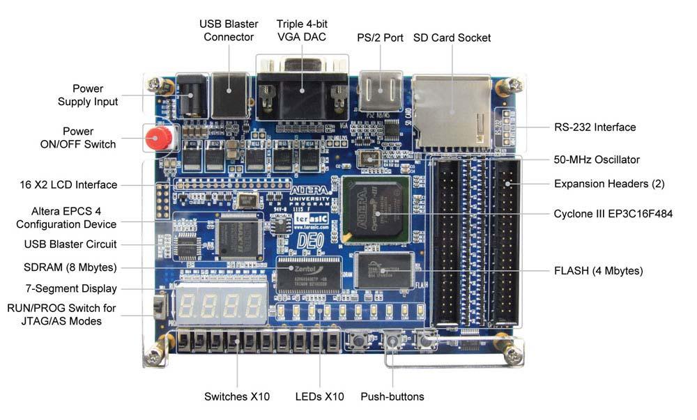
5 DE0 5
6 DE0 6
7 DE0 Switches 7
8 DE0 LEDs 8
9 DE0 7-segment displays 9
10 Developing Digital Logic courses with Altera Technology Tutorial #1
11 Outline Creating projects in Quartus II Targeting a project for a DE0 Board Downloading a circuit onto a DE0 board Compiling and debugging 11

12 Step 1: Start Quartus II Project Navigator Status Window Message Window 12

13 Step 2: Create a New Project Click File Menu Select New Project Wizard This will open a new window where project information can be specified 13

14 Project Name and Directory The project must have a name, which is usually the same as the top-level design entity that will be included in the project. 14

15 Add Source Files to Project The wizard makes it easy to specify which existing files (if any) should be included in the project. Assuming that we do not have any existing files, click Next 15


16 Specify FPGA Device Select the FPGA device on the board Cyclone III Family For DE0 EP3C16F484C6 Cyclone II Family For DE1 EP2C20F484C7 For DE2 EP2C35F672C6 16

17 Additional EDA Tools Specify Tools, in addition to Quartus II, that you will use These are unnecessary for small student designs Leave all entries as <None> Press Next 17

18 New Project Summary A summary of the chosen settings appears in the screen shown in Figure. Press Finish, which returns to the main Quartus II window, but with light specified as the new project, in the display title bar 18
19 Simple Project 19

20 Step 3a: Create Source File Select File > New to get the window in Figure, choose VHDL File, and click OK. This opens the Text Editor window. Specify a name for the file that will be created and select File > Save to open a pop-up box and in the box labeled Save as type choose VHDL File 20

21 Step 3b: Add Source File Select: Assignments > Settings and looks for File item or Project > Add/Remove Files in Project 21


22 Step 4: Assign Pins to connect switches/lights to inputs and outputs of your circuit Click Assignments, then Import Assignments Import file DE0_pin_assignments.qsf Imports locations for predefined port names, such as SW, LEDG, KEY, and others Can be done manually for custom port names 22
23 Step 4: Assign Pins to connect switches/lights to inputs and outputs of your circuit # Pin & Location Assignments # ========================== set_location_assignment PIN_B1 -to LEDG[9] set_location_assignment PIN_B2 -to LEDG[8] set_location_assignment PIN_C2 -to LEDG[7] set_location_assignment PIN_C1 -to LEDG[6] set_location_assignment PIN_E1 -to LEDG[5] set_location_assignment PIN_F2 -to LEDG[4] set_location_assignment PIN_H1 -to LEDG[3] set_location_assignment PIN_J3 -to LEDG[2] set_location_assignment PIN_J2 -to LEDG[1] set_location_assignment PIN_J1 -to LEDG[0] set_location_assignment PIN_D2 -to SW[9] set_location_assignment PIN_E4 -to SW[8] set_location_assignment PIN_E3 -to SW[7] set_location_assignment PIN_H7 -to SW[6] set_location_assignment PIN_J7 -to SW[5] set_location_assignment PIN_G5 -to SW[4] set_location_assignment PIN_G4 -to SW[3] set_location_assignment PIN_H6 -to SW[2] set_location_assignment PIN_H5 -to SW[1] set_location_assignment PIN_J6 -to SW[0] set_location_assignment PIN_F1 -to KEY[2] set_location_assignment PIN_G3 -to KEY[1] set_location_assignment PIN_H2 -to KEY[0] # Pin & Location Assignments # ========================== set_location_assignment PIN_E11 -to HEX0[0] set_location_assignment PIN_F11 -to HEX0[1] set_location_assignment PIN_H12 -to HEX0[2] set_location_assignment PIN_H13 -to HEX0[3] set_location_assignment PIN_G12 -to HEX0[4] set_location_assignment PIN_F12 -to HEX0[5] set_location_assignment PIN_F13 -to HEX0[6] set_location_assignment PIN_D13 -to HEX0[7] set_location_assignment PIN_A15 -to HEX1[6] set_location_assignment PIN_E14 -to HEX1[5] set_location_assignment PIN_B14 -to HEX1[4] set_location_assignment PIN_A14 -to HEX1[3] set_location_assignment PIN_C13 -to HEX1[2] set_location_assignment PIN_B13 -to HEX1[1] set_location_assignment PIN_A13 -to HEX1[0] set_location_assignment PIN_B15 -to HEX1[7] # Pin & Location Assignments # ========================== set_location_assignment PIN_F14 -to HEX2[6] set_location_assignment PIN_B17 -to HEX2[5] set_location_assignment PIN_A17 -to HEX2[4] set_location_assignment PIN_E15 -to HEX2[3] set_location_assignment PIN_B16 -to HEX2[2] set_location_assignment PIN_A16 -to HEX2[1] set_location_assignment PIN_D15 -to HEX2[0] set_location_assignment PIN_A18 -to HEX2[7] set_location_assignment PIN_G15 -to HEX3[6] set_location_assignment PIN_D19 -to HEX3[5] set_location_assignment PIN_C19 -to HEX3[4] set_location_assignment PIN_B19 -to HEX3[3] set_location_assignment PIN_A19 -to HEX3[2] set_location_assignment PIN_F15 -to HEX3[1] set_location_assignment PIN_B18 -to HEX3[0] set_location_assignment PIN_G16 -to HEX3[7] SW: IN STD_LOGIC_VECTOR(N DOWNTO 0); LEDG: OUT STD_LOGIC_VECTOR(N DOWNTO 0); HEX0: OUT STD_LOGIC_VECTOR(0 TO N) x1, x2, f????? 23
 writex begin <= 1'b0; always @ (negedge wrbusy_int) end write0 <= 1'b1; begin write1 <= 1'b0; write0 <= 1'b0;")
24 Step 5: Compile Design // Begin: Write Control (posedge wrbusy_int) begin // Begin: Write Control write0 <= 1'b1; (posedge wrbusy_int) write1 <= 1'b0; begin writex // Begin: <= 1'b0; write0 Write <= 1'b1; Control end write1 always (posedge 1'b0; wrbusy_int) writex begin <= 1'b0; (negedge wrbusy_int) end write0 <= 1'b1; begin write1 <= 1'b0; write0 <= 1'b0; writex (negedge <= wrbusy_int) 1'b0; end beginend write0 <= 1'b0; Verilog, (posedge write0_done) end (negedge wrbusy_int) begin begin write1 <= write0 1'b1; <= 1'b0; (posedge write0_done) beginend write1 <= 1'b1; (posedge write0_done) VHDL begin write1 <= 1'b1; Run the Compiler by selecting Processing > Start Compilation, or by clicking on the toolbar icon that looks like a purple triangle. Successful (or unsuccessful) compilation is indicated in a pop-up box; acknowledge it by clicking OK, which leads to the report shown in next slide Synthesis Placement & Routing Timing & Power Analysis Assembler Report 24

25 Step 6: Examine Compilation Report 25
 mode: a configuration device that includes some flash memory is used to store the configuration data FPGA JTAG mode: flip the RUN/PROG switch into the RUN position and select Tools")
26 Step 7a: Program the DE0 Board FPGA JTAG mode: it will retain its configuration as long as the power remains turned on. Active Serial (AS) mode: a configuration device that includes some flash memory is used to store the configuration data FPGA JTAG mode: flip the RUN/PROG switch into the RUN position and select Tools > Programmer Observe that the configuration file light.sof is listed in the programmer window. If the file is not already listed, then click Add File and select it 26

27 Step 7a: Program the DE0 Board 27

28 Step 7b: Program the DE0 Board Here it is also necessary to specify the programming hardware and the mode that should be used. If not already chosen by default, select JTAG in the Mode box. Also, if the USB-Blaster is not chosen by default, press the Hardware Setup... button and select the USB-Blaster in the window that pops up 28

29 Step 7c: Program the DE0 Board Click on the Program/Configure check box Press Start in the Programmer window; an LED on the board will light up when the configuration data has been downloaded successfully 29
30 Step 8: See your design work on the board Having downloaded the configuration data into the FPGA device, you can now test the implemented circuit. Flip the RUN/PROG switch to RUN position. Try all four valuations of the input variables x1 and x2, by setting the corresponding states of the switches SW1 and SW0. 30
. Select the project you wish to simulate and click OK.")
31 Step 9a: Simulate your design Select Start > All Programs > Altera > University Program > Simulation Tools > QSim to open the Qsim tools. Select File > Open Project to display a popup window in which you can browse your directories and choose a project file (.qpf file). Select the project you wish to simulate and click OK. Generate the node finder files by selecting Processing > Generate Node Finder Files From QSim, open the Waveform Editor window by selecting File > New Simulation Input File. 31

32 Step 9b: Simulate your design Save the file under the name light.vwf; note that this changes the name in the displayed window. Set the desired simulation to run from 0 to 200 ns by selecting Edit > Set End Time and entering 200 ns in the dialog box that pops up. Select View > Fit in Window 32

 into the Name box, or use the Node Finder to")
33 Step 9c: Simulate your design Include the input and output nodes of the circuit to be simulated. Click Edit > Insert > Insert Node or Bus: it is possible to type the name of a signal (pin) into the Name box, or use the Node Finder to search your project for the signals. 33
34 Step 9d: Simulate your design We will now specify the logic values to be used for the input signals x1 and x2 during simulation Click on the waveform for the x1 node and using the Edit > Value command, or via the toolbar, draw the desired waveforms. Commands are available for setting a selected signal to 0, 1, unknown (X), high impedance (Z), weak low (L), weak high (H), a count value (C), an arbitrary value, a random value (R), inverting its existing value (INV), or defining a clock waveform. 34

35 Step 9e: Simulate your design E.g. set x2 to 1 in the time interval 50 to 100 ns. Do this by pressing the mouse at the start of the interval and dragging it to its end, which highlights the selected interval, and choosing the logic value 1 in the toolbar. Observe that the output f is displayed as having an unknown value at this time, which is indicated by a hashed pattern; its value will be determined during simulation. Save the file. 35

36 Step 9f: Simulate your design To perform the functional simulation, return to the QSim Window and select Assign > Simulation Settings... Click the Browse button and select the light.vwf file you created. Choose Functional as the simulation type, and click OK. Select Processing > Generate Simulation Netlist. A simulation run is started by Processing > Start Simulation, 36

37 Step 9g: Simulate your design To perform timing simulation choose Select Assign > Simulation Settings... Choose Timing as the simulation type, and click OK. Run the simulator Observe that there is a delay in producing a change in the signal f from the time when the input signals, x1 and x2, change their values. This delay is due to the propagation delays in the logic element and the wires in the FPGA device 37

38 FSM Viewer Open the FSM Viewer Click Tools Expand Netlist Viewers Click State Machine Viewer 38

39 Examine State Machine 39

40 See the Circuit in RTL Viewer Start the RTL Viewer Click Tools Expand the Netlist Viewers list Click RTL Viewer 40

41 Examine the Circuit 41

42 SignalTap II Embedded Logic Analyzer A soft logic analyzer Instantiate as a module in your design Connects to the board on which a design is running Collects data when a trigger event occurs Displays data on your computer How does it work? 42
![SignalTap II Operation USB-Blaster cable FPGA KEY[0] KEY[1]](/docs-images/82/87015179/images/43-0.jpg "Clock User FSM enable Clock SignalTap Module User Logic Green")
43 SignalTap II Operation USB-Blaster cable FPGA KEY[0] KEY[1] Clock User FSM enable Clock SignalTap Module User Logic Green LEDs 43
44 Altera U. P. Teaching Materials for Digital Logic Available for download: Tutorials Teach students how to use Quartus II, etc. Lab Exercises 10 digital logic exercises Complete with documentation and solutions (both in Verilog and VHDL) IP Cores for DE boards VGA, Audio I/O, and others Great for projects 44

45 Altera U.P. Web Site 45
46 Tutorials Tutorials Getting Started with Altera s DE0 Lab Board Introduction to Quartus II With Verilog, or VHDL, or Schematic Using library modules (LPMs) With Verilog or VHDL Quartus II Simulation With Verilog or VHDL Timing Considerations With Verilog or VHDL Signal Tap II Hardware Debugging Debugging with ModelSim Introduction to Quartus II Acrobat Document 46

47 Digital Logic Lab Exercises Ten lab exercises released From basic logic gates to simple processors: Lab 1: Switches, Lights, and Multiplexers Lab 2: Numbers and Displays Lab 3: Latches, Flip-flops, and Registers Lab 4: Counters Lab 5: Real-time Clock and Timers Lab 6: Adders, Subtractors, and Multipliers Lab 7: Finite State Machines Lab 8: Memory Blocks Lab 9: A Simple Processor Lab 10: An Enhanced Processor 47
48 Lab 1: Switches and Lights Part 1 /* connect switches to lights through FPGA */ LEDG(9) <= SW(9); LEDG(8) <= SW(8);... LEDG <= SW; Part 2 /* build a 2-to-1 multiplexer */ 48
49 Lab 1 Part 2 m <= (NOT(s) AND x) OR (s AND y); Make 3 copies for 3-bit wide 2-to-1 multiplexers, then connect to 3 LEDs Part 3 Build a more complex multiplexer: 2-bit wide 3-to-1 multiplexer 49

50 Lab 1 Part 4 50
51 Lab 1 Select and display one of three characters Part 5 Rotate the word de0 on three displays Part 5 51
52 Lab 1 Part 6 Extend your design from Part V so that is uses all four 7-segment displays on the DE0 board 52
53 Lab 7 FSM Sequence recognizer There is an input w and an output z. Whenever w = 1 or w = 0 for four consecutive clock pulses the value of z has to be 1; otherwise, z = 0. Overlapping sequences are allowed, so that if w = 1 for five consecutive clock pulses the output z will be equal to 1 after the fourth and fifth pulses Part 1 53

54 Lab 7 Part 1 Current State W Next state Z A: B: B: C: C: D: D: E: E: E: F: B: G: B: H: B: I: B: Current State W Next state Z A: F: B: F: C: F: D: F: E: F: F: G: G: H: H: I: I: I: Y_D(1) <= (y_q(0) OR y_q(5) OR y_q(6) OR y_q(7) OR y_q(8)) AND NOT (w);
55 Lab 7 FSM Sequence recognizer Describe the state table for the FSM by using a VHDL CASE statement in a PROCESS block, and use another PROCESS block to instantiate the state flip-flops. Part 2 ARCHITECTURE Behavior OF part2 IS SIGNAL Clock, Resetn, w, z : STD_LOGIC; TYPE State_type IS (A, B, C, D, E, F, G, H, I); SIGNAL y_q, Y_D : State_type; 55
Quartus II Introduction Using Verilog Designs. 1 Introduction. For Quartus II 12.0
 Quartus II Introduction Using Verilog Designs For Quartus II 12.0 1 Introduction This tutorial presents an introduction to the Quartus II CAD system. It gives a general overview of a typical CAD flow for
Tutorial on Quartus II Introduction Using Verilog Code
 Tutorial on Quartus II Introduction Using Verilog Code (Version 15) 1 Introduction This tutorial presents an introduction to the Quartus II CAD system. It gives a general overview of a typical CAD flow
Tutorial on Quartus II Introduction Using Schematic Designs
 Tutorial on Quartus II Introduction Using Schematic Designs (Version 15) 1 Introduction This tutorial presents an introduction to the Quartus II CAD system. It gives a general overview of a typical CAD
1 Introduction 2. 2 Background 3. 3 Getting Started 4. 4 Starting a New Project 6. 5 Design Entry Using VHDL Code 13
 Quartus Prime Introduction Using VHDL Designs For Quartus Prime 17.0 Contents 1 Introduction 2 2 Background 3 3 Getting Started 4 3.1 Quartus Prime Online Help................................................................................................
Quartus II Introduction Using Schematic Design
 Quartus II Introduction Using Schematic Design This tutorial presents an introduction to the Quartus R II CAD system. It gives a general overview of a typical CAD flow for designing circuits that are implemented
Quartus II Introduction Using Verilog Design
 Quartus II Introduction Using Verilog Design This tutorial presents an introduction to the Quartus R II CAD system. It gives a general overview of a typical CAD flow for designing circuits that are implemented
Chapter 2 Getting Hands on Altera Quartus II Software
 Chapter 2 Getting Hands on Altera Quartus II Software Contents 2.1 Installation of Software... 20 2.2 Setting Up of License... 21 2.3 Creation of First Embedded System Project... 22 2.4 Project Building
Quick Tutorial for Quartus II & ModelSim Altera
 Quick Tutorial for Quartus II & ModelSim Altera By Ziqiang Patrick Huang Hudson 213c Ziqiang.huang@duke.edu Download & Installation For Windows or Linux users : Download Quartus II Web Edition v13.0 (ModelSim
NIOS CPU Based Embedded Computer System on Programmable Chip
 1 Objectives NIOS CPU Based Embedded Computer System on Programmable Chip EE8205: Embedded Computer Systems This lab has been constructed to introduce the development of dedicated embedded system based
Introduction to VHDL Design on Quartus II and DE2 Board
 ECP3116 Digital Computer Design Lab Experiment Duration: 3 hours Introduction to VHDL Design on Quartus II and DE2 Board Objective To learn how to create projects using Quartus II, design circuits and
CPE 200L LABORATORY 4: INTRODUCTION TO DE2 BOARD UNIVERSITY OF NEVADA, LAS VEGAS GOALS: BACKGROUND:
 CPE 200L LABORATORY 4: INTRODUCTION TO DE2 BOARD DEPARTMENT OF ELECTRICAL AND COMPUTER ENGINEERING UNIVERSITY OF NEVADA, LAS VEGAS GOALS: Getting familiar with DE2 board installation, properties, usage.
Laboratory Exercise 7
 Laboratory Exercise 7 Finite State Machines This is an exercise in using finite state machines. Part I We wish to implement a finite state machine (FSM) that recognizes two specific sequences of applied
Terasic DE0 Field Programmable Gate Array (FPGA) Development Board
 Development Board") Lecture FPGA-01 DE0 FPGA Development Board and Quartus II 9.1 FPGA Design Software Terasic DE0 Field Programmable Gate Array (FPGA) Development Board 1 May 16, 2013 3 Layout and Components of DE0 May 16,
Lecture FPGA-01 DE0 FPGA Development Board and Quartus II 9.1 FPGA Design Software Terasic DE0 Field Programmable Gate Array (FPGA) Development Board 1 May 16, 2013 3 Layout and Components of DE0 May 16,
Advanced Electronics Lab.
 College of Engineering Course Book of 2010-2011 Advanced Electronics Lab. Mr. Araz Sabir Ameen M.Sc. in Electronics & Communications ALTERA DE2 Development and Education Board DE2 Package: The DE2 package
ECE 3610 Microprocessing Systems Lab #1 Verilog Design of the TOC Using Quartus II
 ECE 3610 Microprocessing Systems Lab #1 Verilog Design of the TOC Using Quartus II This lab manual presents an introduction to the Quartus II Computer Aided Design (CAD) system. This manual gives step-by-step
EMT1250 LABORATORY EXPERIMENT. EXPERIMENT # 6: Quartus II Tutorial and Practice. Name: Date:
 EXPERIMENT # 6: Quartus II Tutorial and Practice Name: Date: Equipment/Parts Needed: Quartus II R Web Edition V9.1 SP2 software by Altera Corporation USB drive to save your files Objective: Learn how to
Laboratory Exercise 3 Comparative Analysis of Hardware and Emulation Forms of Signed 32-Bit Multiplication
 Laboratory Exercise 3 Comparative Analysis of Hardware and Emulation Forms of Signed 32-Bit Multiplication Introduction All processors offer some form of instructions to add, subtract, and manipulate data.
EMT1250 LABORATORY EXPERIMENT. EXPERIMENT # 7: VHDL and DE2 Board. Name: Date:
 EXPERIMENT # 7: VHDL and DE2 Board Name: Date: Equipment/Parts Needed: Quartus II R Web Edition V9.1 SP2 software by Altera Corporation USB drive to save your files Objective: Learn how to create and modify
UNIVERSITI MALAYSIA PERLIS
 UNIVERSITI MALAYSIA PERLIS SCHOOL OF COMPUTER & COMMUNICATIONS ENGINEERING EKT 124 LABORATORY MODULE INTRODUCTION TO QUARTUS II DESIGN SOFTWARE : INTRODUCTION TO QUARTUS II DESIGN SOFTWARE OBJECTIVES To
FPGA Introductory Tutorial: Part 1
 FPGA Introductory Tutorial: Part 1 This tutorial is designed to assist in learning the basics of the Altera Quartus II v9.0 software. Part 1 of the tutorial will cover the basics of creating a Project,
Tutorial 2 Implementing Circuits in Altera Devices
 Appendix C Tutorial 2 Implementing Circuits in Altera Devices In this tutorial we describe how to use the physical design tools in Quartus II. In addition to the modules used in Tutorial 1, the following
NIOS CPU Based Embedded Computer System on Programmable Chip
 NIOS CPU Based Embedded Computer System on Programmable Chip 1 Lab Objectives EE8205: Embedded Computer Systems NIOS-II SoPC: PART-I This lab has been constructed to introduce the development of dedicated
Tutorial for Altera DE1 and Quartus II
 Tutorial for Altera DE1 and Quartus II Qin-Zhong Ye December, 2013 This tutorial teaches you the basic steps to use Quartus II version 13.0 to program Altera s FPGA, Cyclone II EP2C20 on the Development
Contents. Appendix B HDL Entry Tutorial 2 Page 1 of 14
 Appendix B HDL Entry Tutorial 2 Page 1 of 14 Contents Appendix B HDL Entry Tutorial 2...2 B.1 Getting Started...2 B.1.1 Preparing a Folder for the Project...2 B.1.2 Starting Quartus II...2 B.1.3 Creating
UNIVERSITY OF CALIFORNIA, DAVIS Department of Electrical and Computer Engineering. EEC180A DIGITAL SYSTEMS I Winter 2015
 UNIVERSITY OF CALIFORNIA, DAVIS Department of Electrical and Computer Engineering EEC180A DIGITAL SYSTEMS I Winter 2015 LAB 1: Introduction to Quartus II Schematic Capture and ModelSim Simulation This
Laboratory Exercise 8
 Laboratory Exercise 8 Memory Blocks In computer systems it is necessary to provide a substantial amount of memory. If a system is implemented using FPGA technology it is possible to provide some amount
CSEE W4840 Embedded System Design Lab 1
 CSEE W4840 Embedded System Design Lab 1 Stephen A. Edwards Due January 31, 2008 Abstract Learn to use the Altera Quartus development envrionment and the DE2 boards by implementing a small hardware design
DE2 Board & Quartus II Software
 January 23, 2015 Contact and Office Hours Teaching Assistant (TA) Sergio Contreras Office Office Hours Email SEB 3259 Tuesday & Thursday 12:30-2:00 PM Wednesday 1:30-3:30 PM contre47@nevada.unlv.edu Syllabus
The development board used in this class is ALTERA s DE The board provides the following hardware:
 Lab 1 The goal of this lab is to get familiar with the mechanics of designing digital systems using VHDL and ALTERA s FPGAs. The development board used in this class is ALTERA s DE2-115. The board provides
NIOS CPU Based Embedded Computer System on Programmable Chip
 NIOS CPU Based Embedded Computer System on Programmable Chip EE8205: Embedded Computer Systems NIOS-II SoPC: PART-II 1 Introduction This lab has been constructed to introduce the development of dedicated
Introduction to the Altera SOPC Builder Using Verilog Design
 Introduction to the Altera SOPC Builder Using Verilog Design This tutorial presents an introduction to Altera s SOPC Builder software, which is used to implement a system that uses the Nios II processor
SOPC LAB1. I. Introduction. II. Lab contents. 4-bit count up counter. Advanced VLSI Due Wednesday, 01/08/2003
 SOPC LAB1 I. Introduction The purpose of this lab is to familiarize you with all the items in the kit. This tutorial tells you how to develop FPGA system in Quartus II. You are ready to begin using the
SignalTap II with Verilog Designs. 1 Introduction. For Quartus II 13.1
 SignalTap II with Verilog Designs For Quartus II 13.1 1 Introduction This tutorial explains how to use the SignalTap II feature within Altera s Quartus II software. The SignalTap II Embedded Logic Analyzer
Introduction to the Altera SOPC Builder Using Verilog Designs. 1 Introduction
 Introduction to the Altera SOPC Builder Using Verilog Designs 1 Introduction This tutorial presents an introduction to Altera s SOPC Builder software, which is used to implement a system that uses the
Engineering 303 Digital Logic Design Spring 2017
 Engineering 303 Digital Logic Design Spring 2017 LAB 1 Introduction to Combo Logic and Quartus Deliverables: 0) A Simple Verilog Combinatorial Circuit 1) A Simple Block Diagram Combinatorial Circuit 2)
NOTE: This tutorial contains many large illustrations. Page breaks have been added to keep images on the same page as the step that they represent.
 CSE 352 Tutorial # 4 Synthesizing onto an FPGA Objectives This tutorial will walk you through the steps of implementing a design made in Active-HDL onto the Altera Cyclone II FPGA NOTE: This tutorial contains
QuartusII.doc 25/02/2005 Page 1
 1 Start Icon... 2 1.1 The Quartus II Screen... 2 2 Project creation... 2 3 Schematic entry... 5 3.1 Create new drawing... 5 3.2 Symbol selection... 7 3.3 Placement of an AND gate... 8 3.4 Deleting a symbol...
University of Florida EEL 3701 Dr. Eric M. Schwartz Madison Emas, TA Department of Electrical & Computer Engineering Revision 1 5-Jun-17
 Page 1/14 Example Problem Given the logic equation Y = A*/B + /C, implement this equation using a two input AND gate, a two input OR gate and two inverters under the Quartus environment. Upon completion
University of Florida EEL 3701 Dr. Eric M. Schwartz Department of Electrical & Computer Engineering Revision 0 12-Jun-16
 Page 1/14 Quartus Tutorial with Basic Graphical Gate Entry and Simulation Example Problem Given the logic equation Y = A*/B + /C, implement this equation using a two input AND gate, a two input OR gate
2 nd Year Laboratory. Experiment: FPGA Design with Verilog. Department of Electrical & Electronic Engineering. Imperial College London.
 Department of Electrical & Electronic Engineering 2 nd Year Laboratory Experiment: FPGA Design with Verilog Objectives By the end of this experiment, you should know: How to design digital circuits using
Tutorial 3. Appendix D. D.1 Design Using Verilog Code. The Ripple-Carry Adder Code. Functional Simulation
 Appendix D Tutorial 3 This tutorial introduces more advanced capabilities of the Quartus II system. We show how Verilog code is organized and compiled and illustrate how multibit signals are represented
University of Massachusetts Amherst Computer Systems Lab 2 (ECE 354) Spring Lab 1: Using Nios 2 processor for code execution on FPGA
 Spring Lab 1: Using Nios 2 processor for code execution on FPGA") University of Massachusetts Amherst Computer Systems Lab 2 (ECE 354) Spring 2007 Lab 1: Using Nios 2 processor for code execution on FPGA Objectives: After the completion of this lab: 1. You will understand
University of Massachusetts Amherst Computer Systems Lab 2 (ECE 354) Spring 2007 Lab 1: Using Nios 2 processor for code execution on FPGA Objectives: After the completion of this lab: 1. You will understand
CSEE W4840 Embedded System Design Lab 1
 CSEE W4840 Embedded System Design Lab 1 Stephen A. Edwards Due February 2, 2009 Abstract Learn to use the Altera Quartus development envrionment and the DE2 boards by implementing a small hardware design
CSEE W4840 Embedded System Design Lab 1
 CSEE W4840 Embedded System Design Lab 1 Stephen A. Edwards Due February 3, 2011 Abstract Learn to use the Altera Quartus development envrionment and the DE2 boards by implementing a small hardware design
Using ModelSim to Simulate Logic Circuits in VHDL Designs. 1 Introduction. For Quartus II 13.0
 Using ModelSim to Simulate Logic Circuits in VHDL Designs For Quartus II 13.0 1 Introduction This tutorial is a basic introduction to ModelSim, a Mentor Graphics simulation tool for logic circuits. We
EE 231 Fall Lab 1: Introduction to Verilog HDL and Altera IDE
 Lab 1: Introduction to Verilog HDL and Altera IDE Introduction In this lab you will design simple circuits by programming the Field-Programmable Gate Array (FPGA). At the end of the lab you should be able
LAB 2: INTRODUCTION TO LOGIC GATE AND ITS BEHAVIOUR
 LAB 2: INTRODUCTION TO LOGIC GATE AND ITS BEHAVIOUR OBJECTIVE 1. To verify the operation of OR, AND, INVERTER gates 2. To implement the operation of NAND and NOR gate 3. To construct a simple combinational
Laboratory Exercise 3
 Laboratory Exercise 3 Latches, Flip-flops, and egisters The purpose of this exercise is to investigate latches, flip-flops, and registers. Part I Altera FPGAs include flip-flops that are available for
University of Massachusetts Amherst Computer Systems Lab 1 (ECE 354) LAB 1 Reference Manual
 LAB 1 Reference Manual") University of Massachusetts Amherst Computer Systems Lab 1 (ECE 354) LAB 1 Reference Manual Lab 1: Using NIOS II processor for code execution on FPGA Objectives: 1. Understand the typical design flow in
University of Massachusetts Amherst Computer Systems Lab 1 (ECE 354) LAB 1 Reference Manual Lab 1: Using NIOS II processor for code execution on FPGA Objectives: 1. Understand the typical design flow in
ECSE-323 Digital System Design. Lab #1 Using the Altera Quartus II Software Fall 2008
 1 ECSE-323 Digital System Design Lab #1 Using the Altera Quartus II Software Fall 2008 2 Introduction. In this lab you will learn the basics of the Altera Quartus II FPGA design software through following
Laboratory 4 Design a Muti-bit Counter and Programming a FPGA
 Laboratory 4 Design a Muti-bit Counter and Programming a FPGA For your report: The problem written in English The flowchart or function table to solve the problem if it is necessary The design entry included
EE 231 Fall EE 231 Lab 2
 EE 231 Lab 2 Introduction to Verilog HDL and Quartus In the previous lab you designed simple circuits using discrete chips. In this lab you will do the same but by programming the CPLD. At the end of the
IMPLEMENTING COUNTERS
 EECS:6660:0xxField Programmable Gate Arrays s11l1_fpga.fm - 1 Lab Assignment #1 Due Thursday, March 31 2011 IMPLEMENTING COUNTERS 1. OBJECTIVES - learning the VHDL implementation process using Language
CSC / EE Digital Systems Design. Summer Sample Project Proposal 01
 THE CATHOLIC UNIVERSITY OF AMERICA SCHOOL OF ENGINEERING DEPARTMENT OF ELECTRICAL ENGINEERING AND COMPUTER SCIENCE CSC / EE 519-01 Digital Systems Design Summer 2013 Sample Project Proposal 01 Thursday
Using ModelSim to Simulate Logic Circuits for Altera FPGA Devices
 Using ModelSim to Simulate Logic Circuits for Altera FPGA Devices This tutorial is a basic introduction to ModelSim, a Mentor Graphics simulation tool for logic circuits. We show how to perform functional
SCHEMATIC DESIGN IN QUARTUS
 SCHEMATIC DESIGN IN QUARTUS Consider the design of a three-bit prime number detector. Figure 1 shows the block diagram and truth table. The inputs are binary signals A, B, and C while the output is binary
PRELAB! Read the entire lab, and complete the prelab questions (Q1- Q3) on the answer sheet before coming to the laboratory.
 on the answer sheet before coming to the laboratory.") PRELAB! Read the entire lab, and complete the prelab questions (Q1- Q3) on the answer sheet before coming to the laboratory. 1.0 Objectives In this lab you will get familiar with the concept of using the
PRELAB! Read the entire lab, and complete the prelab questions (Q1- Q3) on the answer sheet before coming to the laboratory. 1.0 Objectives In this lab you will get familiar with the concept of using the
EMT1250 LABORATORY EXPERIMENT. EXPERIMENT # 10: Implementing Binary Adders. Name: Date:
 EXPERIMENT # 10: Implementing Binary Adders Name: Date: Equipment/Parts Needed: PC (Altera Quartus II V9.1 installed) DE-2 board Objective: Design a half adder by extracting the Boolean equation from a
Lab 2 EECE473 Computer Organization & Architecture University of Maine
 Lab 2: Verilog Programming Instructor: Yifeng Zhu 50 Points Objectives: 1. Quatus II Programming assignment: PIN assignments, LEDs, switches; 2. Download and test the design on Altera DE2 board 3. Create
Lab 2: Introduction to Verilog HDL and Quartus
 Lab 2: Introduction to Verilog HDL and Quartus September 16, 2008 In the previous lab you designed simple circuits using discrete chips. In this lab you will do the same but by programming the CPLD. At
E85: Digital Design and Computer Engineering Lab 2: FPGA Tools and Combinatorial Logic Design
 E85: Digital Design and Computer Engineering Lab 2: FPGA Tools and Combinatorial Logic Design Objective The purpose of this lab is to learn to use Field Programmable Gate Array (FPGA) tools to simulate
Simulating a Design Circuit Using Qsim
 Simulating a Design Circuit Using Qsim 1. Start Qsim From version 11.1, Quartus II provides another simulating tool called Qsim. Qsim is bundled with both subscript edition and web edition of Quartus II.
Introduction to Simulation of VHDL Designs Using ModelSim Graphical Waveform Editor. 1 Introduction. For Quartus Prime 16.1
 Introduction to Simulation of VHDL Designs Using ModelSim Graphical Waveform Editor For Quartus Prime 16.1 1 Introduction This tutorial provides an introduction to simulation of logic circuits using the
Laboratory Exercise 5
 Laboratory Exercise 5 Bus Communication The purpose of this exercise is to learn how to communicate using a bus. In the designs generated by using Altera s SOPC Builder, the Nios II processor connects
Physics 536 Spring Illustrating the FPGA design process using Quartus II design software and the Cyclone II FPGA Starter Board.
 Physics 536 Spring 2009 Illustrating the FPGA design process using Quartus II design software and the Cyclone II FPGA Starter Board. Digital logic: Equivalent to a large number of discrete logic elements
Chapter 2: Hardware Design Flow Using Verilog in Quartus II
 Chapter 2: Hardware Design Flow Using Verilog in Quartus II 2.1 Introduction to Quartus II System Development Software This chapter is an introduction to the Quartus II software that will be used for analysis
University of California, Davis Department of Electrical and Computer Engineering. Lab 1: Implementing Combinational Logic in the MAX10 FPGA
 1 University of California, Davis Department of Electrical and Computer Engineering EEC180B DIGITAL SYSTEMS II Winter Quarter 2018 Lab 1: Implementing Combinational Logic in the MAX10 FPGA Objective: This
Altera Quartus II Tutorial ECE 552
 Altera Quartus II Tutorial ECE 552 Quartus II by Altera is a PLD Design Software which is suitable for high-density Field-Programmable Gate Array (FPGA) designs, low-cost FPGA designs, and Complex Programmable
Lab 3. Advanced VHDL
 Lab 3 Advanced VHDL Lab 3 Advanced VHDL This lab will demonstrate many advanced VHDL techniques and how they can be used to your advantage to create efficient VHDL code. Topics include operator balancing,
Introduction to the Altera Qsys System Integration Tool. 1 Introduction. For Quartus Prime 15.1
 Introduction to the Altera Qsys System Integration Tool For Quartus Prime 15.1 1 Introduction This tutorial presents an introduction to Altera s Qsys system integration tool, which is used to design digital
Digital Systems Laboratory
 2012 Fall CSE140L Digital Systems Laboratory by Dr. Choon Kim CSE Department UCSD 1 Welcome to CSE140L! 2 3-way Light Controller, 2-1 MUX, Majority Detector, 7- seg Display, Binary-to- Decimal converter.
Chip Design with FPGA Design Tools
 Chip Design with FPGA Design Tools Intern: Supervisor: Antoine Vazquez Janusz Zalewski Florida Gulf Coast University Fort Myers, FL 33928 V1.9, August 28 th. Page 1 1. Introduction FPGA is abbreviation
EXPERIMENT 1. INTRODUCTION TO ALTERA
 EXPERIMENT 1. INTRODUCTION TO ALTERA I. Introduction I.I Objectives In this experiment, you will learn computer aided digital design and verification of it using Field Programmable Gate Arrays (FPGA).
COSC 3215 Embedded Systems Laboratory
 COSC 3215 Embedded Systems Laboratory Lab 5 The Altera, Verilog and QuartusII Introduction This lab is an introduction to the Altera FPGA development board and the accompanying FPGA programming environment
DKAN0011A Setting Up a Nios II System with SDRAM on the DE2
 DKAN0011A Setting Up a Nios II System with SDRAM on the DE2 04 November 2009 Introduction This tutorial details how to set up and instantiate a Nios II system on Terasic Technologies, Inc. s DE2 Altera
CHAPTER 1 INTRODUCTION Features About the KIT Getting Help... 7 CHAPTER 2 DE0-NANO BOARD ARCHITECTURE...
 1 CONTENTS CHAPTER 1 INTRODUCTION... 5 1.1 Features... 5 1.2 About the KIT... 7 1.3 Getting Help... 7 CHAPTER 2 DE0-NANO BOARD ARCHITECTURE... 8 2.1 Layout and Components... 8 2.2 Block Diagram of the
My First FPGA for Altera DE2-115 Board
 My First FPGA for Altera DE2-115 Board 數位電路實驗 TA: 吳柏辰 Author: Trumen Outline Complete Your Verilog Design Assign The Device Add a PLL Megafunction Assign the Pins Create a Default TimeQuest SDC File Compile
Quartus II Tutorial. September 10, 2014 Quartus II Version 14.0
 Quartus II Tutorial September 10, 2014 Quartus II Version 14.0 This tutorial will walk you through the process of developing circuit designs within Quartus II, simulating with Modelsim, and downloading
Altera DE1 Board DE1. Development and Education Board. User Manual. Copyright 2006 Altera Corporation
 Altera DE1 Board DE1 Development and Education Board User Manual Version 1.1 Copyright 2006 Altera Corporation Chapter 2 Altera DE1 Board This chapter presents the features and design characteristics of
Laboratory 4 Design a Muti-bit Counter
 Laboratory 4 Design a Muti-bit Counter Background A. Approach I: Design 3-bit counter with and clear T-type flip-flop is shown in Figure 1. A T flip-flop is obtained from a JK flip-flop by tying the J
Lecture 1: Introduction Course arrangements Recap of basic digital design concepts EDA tool demonstration
 TKT-1426 Digital design for FPGA, 6cp Fall 2011 http://www.tkt.cs.tut.fi/kurssit/1426/ Tampere University of Technology Department of Computer Systems Waqar Hussain Lecture Contents Lecture 1: Introduction
CSE P567 - Winter 2010 Lab 1 Introduction to FGPA CAD Tools
 CSE P567 - Winter 2010 Lab 1 Introduction to FGPA CAD Tools This is a tutorial introduction to the process of designing circuits using a set of modern design tools. While the tools we will be using (Altera
CME341 Laboratory Manual
 CME341 Laboratory Manual Created by Eric Salt Created June 30, 2012 Revised Nov. 30, 2012 Revised Dec. 13, 2012 (to end of Lab 2) Revised Dec. 18, 2012 (to end of Lab 3) Revised Jan. 13, 2013 (to end of
ENEE245 Digital Circuits and Systems Lab Manual
 ENEE245 Digital Circuits and Systems Lab Manual Department of Engineering, Physical & Computer Sciences Montgomery College Version 1.1 Copyright Prof. Lan Xiang (Do not distribute without permission) 1
Quartus II Version 14.0 Tutorial Created September 10, 2014; Last Updated January 9, 2017
 Quartus II Version 14.0 Tutorial Created September 10, 2014; Last Updated January 9, 2017 This tutorial will walk you through the process of developing circuit designs within Quartus II, simulating with
FPGA for Software Engineers
 FPGA for Software Engineers Course Description This course closes the gap between hardware and software engineers by providing the software engineer all the necessary FPGA concepts and terms. The course
Making Qsys Components. 1 Introduction. For Quartus II 13.0
 Making Qsys Components For Quartus II 13.0 1 Introduction The Altera Qsys tool allows a digital system to be designed by interconnecting selected Qsys components, such as processors, memory controllers,
TLL5000 Electronic System Design Base Module. Getting Started Guide, Ver 3.4
 TLL5000 Electronic System Design Base Module Getting Started Guide, Ver 3.4 COPYRIGHT NOTICE The Learning Labs, Inc. ( TLL ) All rights reserved, 2008 Reproduction in any form without permission is prohibited.
CHAPTER 1 INTRODUCTION... 1 CHAPTER 2 ASSIGN THE DEVICE... 7 CHAPTER 3 DESIGN ENTRY CHAPTER 4 COMPILE AND VERIFY YOUR DESIGN...
 CONTENTS CHAPTER 1 INTRODUCTION... 1 1.1 DESIGN FLOW... 1 1.2 BEFORE YOU BEGIN... 2 1.3 WHAT YOU WILL LEARN... 6 CHAPTER 2 ASSIGN THE DEVICE... 7 2.1 ASSIGN THE DEVICE... 7 CHAPTER 3 DESIGN ENTRY... 11
Actel Libero TM Integrated Design Environment v2.3 Structural Schematic Flow Design Tutorial
 Actel Libero TM Integrated Design Environment v2.3 Structural Schematic Flow Design Tutorial 1 Table of Contents Design Flow in Libero TM IDE v2.3 Step 1 - Design Creation 3 Step 2 - Design Verification
DOWNLOADING DESIGNS TO THE ALTERA DE10-LITE FPGA
 DOWNLOADING DESIGNS TO THE ALTERA DE10-LITE FPGA Consider the design of a three-bit prime number detector completed in the MSOE schematic entry tutorial. Figure 1 shows the block diagram and truth table.
CHAPTER 3 METHODOLOGY. 3.1 Analysis of the Conventional High Speed 8-bits x 8-bits Wallace Tree Multiplier
 CHAPTER 3 METHODOLOGY 3.1 Analysis of the Conventional High Speed 8-bits x 8-bits Wallace Tree Multiplier The design analysis starts with the analysis of the elementary algorithm for multiplication by
ENEE245 Digital Circuits and Systems Lab Manual
 ENEE245 Digital Circuits and Systems Lab Manual Department of Engineering, Physical & Computer Sciences Montgomery College Modified Fall 2017 Copyright Prof. Lan Xiang (Do not distribute without permission)
Introduction to Electronics Workbench
 Introduction to Electronics Workbench Electronics Workbench (EWB) is a design tool that provides you with all the components and instruments to create board-level designs on your PC. The user interface
1.1 Features Block Diagram of the DE0-Nano Board Power-up the DE0-Nano Board Configuring the Cyclone IV FPGA...
 1 CONTENTS CHAPTER 1 INTRODUCTION... 5 1.1 Features...5 1.2 About the KIT...7 1.3 Getting Help...7 CHAPTER 2 DE0-NANO BOARD ARCHITECTURE... 8 2.1 Layout and Components...8 2.2 Block Diagram of the DE0-Nano
E85: Digital Design and Computer Architecture J. Spjut and R. Wang Spring 2014
 E85: Digital Design and Computer Architecture J. Spjut and R. Wang Spring 2014 Lab 1: Full Adder Introduction In this lab you will design a simple digital circuit called a full adder. Along the way, you
Using Library Modules in VHDL Designs
 Using Library Modules in VHDL Designs This tutorial explains how Altera s library modules can be included in VHDL-based designs, which are implemented by using the Quartus R II software. Contents: Example
Xilinx Tutorial Basic Walk-through
 Introduction to Digital Logic Design with FPGA s: Digital logic circuits form the basis of all digital electronic devices. FPGAs (Field Programmable Gate Array) are large programmable digital electronic
Altera Technical Training Quartus II Software Design
 Altera Technical Training Quartus II Software Design Exercises Quartus II Software Design Series: Foundation 2 Quartus II Software Design Series: Foundation Exercises Exercise 1 3 Exercises Quartus II