On the Decreasing Significance of Large Standard Cells in Technology Mapping
|
|
|
- Myles George
- 5 years ago
- Views:
Transcription
1 On the Decreasing Significance of Standard s in Technology Mapping Jae-sun Seo, Igor Markov, Dennis Sylvester, and David Blaauw Department of EECS, University of Michigan, Ann Arbor, MI {jseo,imarkov,dmcs,blaauw}@umich.edu ABSTRACT Technology scaling reduces gate s while s may increase. Our work studies the interaction of this phenomenon with technology mapping and its impact on modern EDA flows. In particular, we demonstrate that the use of larger standard cells increases the number of long s and may undermine circuit optimization at 65nm and below. Experiments with 130nm, 90nm, 65nm, and 45nm industrial CMOS technology suggest that limiting the use of larger standard cells in technology mapping becomes more effective at 65nm and 45nm node, resulting in up to 12% improvement in critical on large benchmark circuits. 1. INTRODUCTION Over several decades, technology mapping has been extremely useful for reducing the device of complex logic. Furthermore, recent research in Boolean matching [1-2] accomplished dramatic efficiency improvements for function matching, facilitating new technology mapping algorithms that can deal with 10-input gates. However, extending these algorithms with proper models of circuit and validating them with respect to recent technology nodes remains a major research challenge. While technology mapping seeks to minimize device count, the bulk of critical has shifted from gates to s in the last 5 years. In particular, the number of repeaters required is exponentially increasing with each technology step [3-4], and 10~15% of gates in large microprocessor chips are buffers that break down long interconnects. Extensive literature exists on optimal buffering [5-7] that employs fairly accurate modeling, but does not attempt logic restructuring. Our work is motivated by the apparent dichotomy between (1) the literature on buffer insertion that improves circuit performance by adding a large number of one-input oneoutput gates (buffers and inverters) that do not perform any logic operation, and (2) the literature on functional technology mapping, which clusters logic into 5-15 input gates, improving, but does not evaluate overall circuit performance with respect to current technology nodes. Previous literature [8-11] suggests that technology mapping must interact with placement of the standard cells and use accurate interconnect models for performance optimization. These works improved the critical through either integration of layout information in early logic synthesis stage [8-9] or iterative re-synthesis with placement information [10-11], but they have not considered the impact of technology mapping on global buffer counts and the overall circuit performance after place-and-route optimizations. This paper proposes to, ironically, undo technology mapping for high-speed designs through reducing the components in the critical of large circuits. Foregoing aggressive technology mapping and using a large number of standard cells (but of smaller size) will eliminate the need for excessive buffers during post-placement timing optimization. The discussions and experiments in this work also consider coupling capacitance between adjacent s which dominates the capacitance in most advanced technologies, and we attempt to reduce the parallel run of neighboring s. Recent work [15] points out that conglomerating small cells into a large cell may produce non-monotonic interconnects which adversely affect and routability as illustrated in Figure 1. By limiting the use of large standard cells, our approach inherently blocks the occurrence of this disadvantageous technology mapping, and results in a number of shorter monotonic s. Our considerations and conclusions are intended for ASIC/SoC designs rather than FPGA designs. Since programmable interconnect is uniformly buffered and has linear in FPGA designs, s do not significantly depend on whether long nets are broken into shorter segments. On the other hand, technology mapping Figure 1: Indiscriminate technology mapping may produce longer s, adversely affecting and routing congestion.


.")
2 into LUTs is an important and difficult task. Therefore, in FPGAs, technology mapping still remains useful. The remainder of this paper is organized as follows. In section 2, a clean experiment is analyzed with a simple combinational logic block and a long. Section 3 evaluates the impact of standard cell libraries on circuit, shows the experimental results, and explains the observations. Section 4 summarizes this paper. 2. ANALYSIS OF SINGLE PATHS As a proof of concept, we conducted a simple experiment as depicted in Figure 2. As a baseline for comparison, input NAND gates drive a M5 minimum-pitch 5mm, which is optimally repeated in 65nm technology. Traditionally, we would have the combinational logic placed in a denser cluster for minimum as shown in Figure 2(a). Instead, however, we spread out the 16 NAND gates regularly along the interconnect to implement the logic and also serve as repeaters in Figure 2(b). These distributed NAND gates eliminate long s and the need for repeaters, resulting in actually better performance. This effect could be exploited by decomposing the logic into more gates, i.e., undoing technology mapping. In Figure 2(c), the long is divided more finely with more logic gates (24 2-input NANDs) for the same functionality. te that, in Figure 2(a)-(c), the inputs of the NAND gates which are not in the critical are tied to Vdd for worst-case rising s. HSPICE simulation is done with industrial 65nm CMOS technology, where all three schemes are swept with sizing, and the optimal energy versus results are shown in Figure 3. Comparing to scheme (a) at iso-energy of 1.1pJ, scheme (b) achieves 13% reduction and scheme (c) achieves 18% reduction. Overall, (c) improves the energy- curve of (a) by a significant amount. At these points, Figure 4 shows a breakdown of the three Figure 3: Energy versus comparison for the three different schemes in Figure 2. schemes. By spreading out the NAND gates in (b), logic gate is increased since the load capacitance of the NAND gates is increased due to s, but the repeater portion is eliminated and the overall is reduced by 13%. Through undoing technology mapping in (c), is further reduced due to fine chopping of s and gate also slightly decreased due to reduced load capacitance. Interestingly, if long s are present in the circuit, spreading out the gates and using more gates to implement a given logic could actually improve since they convert back to logic. One possible drawback of this approach is that the inputs to the NAND gates in the middle of the have to be routed to the intermediate placement locations, but the surrounding logic gates could be restructured and placed nearby the middle of the. We scrutinized this in the following section by performing synthesis, placement and routing on large benchmarks. (a) (b) (c) Figure 2: Three schemes for comparison of single s (a) Logic block (16 3-input NANDs) driving an optimally repeated 5mm (b) 16 3-input NANDs are placed along the (c) 16 3-input NANDs are decomposed into input NANDs and placed along the. Figure 4: Delay breakdown (logic, repeater, and ) of the three schemes in Figure 2 at iso-energy of 1.1pJ.


![benchmark circuits from IWLS 2005 [12] were](/docs-images/93/112210896/images/3-16.jpg "used (s35932 from ISCAS family and the rest")


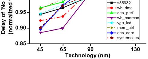
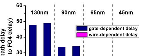
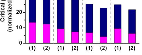
3 3. EVALUATING UTILITY OF LARGE CELLS IN TECHNOLOGY MAPPING To evaluate the utility of technology mapping for general circuits in scaled technologies, we compare pairs of libraries for several benchmarks with each technology. scheme uses original standard cell library without any restriction, while s scheme is confined to the library where there are only 1-input and 2-input gates available. 3.1 Methodology Figure 5 shows the flow chart for both approaches. Starting from the same behavioral netlist, logic synthesis (Synopsys Design Compiler sp2) is applied for each scheme with a restriction on the s scheme to use only 1-input or 2-input standard cells. After logic synthesis, the structural netlist goes through timing-driven placement, physical synthesis, and timing-driven routing (Cadence SoC Encounter 6.1.2). Post-placement logic restructuring is executed if necessary, but the restriction on the number of inputs of gates still holds in the s scheme. Finally, timing analysis is performed for both approaches with all back-end parasitics including coupling capacitance. This procedure was done for industrial 130nm, 90nm, 65nm, and 45nm technologies, and benchmark circuits from IWLS 2005 [12] were used (s35932 from ISCAS family and the rest of them from OpenCores family). In the overall flow, the proposed scheme does not add any intermediate steps or iterations to the baseline. In fact, our approach seeks to reduce resource utilization (less standard cells from the library) while also improving. Figure 6: comparison of IWLS benchmarks using and s approach in 130nm, 90nm, 65nm, and 45nm technology. 3.2 Experimental Results One expects the s approach to increase the gate count due to a more limited standard cell library. However, the critical could actually benefit from more gates since both the capacitance and the number of required buffers are reduced. Figure 6 compares the critical between and s configurations for eight benchmarks. Delay of s scheme is normalized to that of scheme. The monotonic trend shown in Figure 6 illustrates the decreasing utility of large standard cells in technology mapping for more advanced technologies. At 65nm and 45nm technology, discarding large standard cells (3-inputs or more) gave better results (1-12%) in critical Figure 5: Flow chart for the methodology of and s. Figure 7: breakdown (gate-dependent and -dependent ) of benchmark wb_conmax for (1) and (2) s approach across four technology nodes.
4 Table 1: Detailed comparison of the benchmarks for and s scheme on critical, average (=total routed / count), inserted buffer count, total standard cell count, capacitance, and total standard cell is shown for (a) 65nm and (b) 45nm technology. (FO4) (μm) Buffer Wire capacitance count / total (ff) cell count total coupling (a) 65nm (μm 2 ) s (vs. ) Buffer count Wire capacitance / total cell count total coupling s / % +3.4% -10% / +35% +14% +12% +10.6% wb_dma / % -15.8% -19% / +19% -5% -8% +4.0% des_perf / % -11.3% -44% / +12% -2% -4% -1.6% wb_conmax / % -45.0% -15% / +73% -21% -26% +18.3% vga_lcd / % -23.5% -5% / + 32% -9% -18% +12.9% mem_ctrl / % -23.1% -27% / +37% +2% -1% +6.5% aes_core / % -22.9% -11% / +19% -15% -22% -9.8% systemcaes / % -19.0% -27% / +20% +7% +2% +20.9% Average -3.8% -19.7% -20% / +31% -4% -8% +7.7% (FO4) (μm) Buffer Wire capacitance count / total (ff) cell count total coupling (b) 45nm (μm 2 ) s (vs. ) Buffer count Wire capacitance / total cell count total coupling s / % -14.5% -5.3% / +18% +8% +7% +7.5% wb_dma / % -12.5% -13% / +6% -9% -12% -1.7% des_perf / % -16.7% -27% / +20% -4% -10% +3.1% wb_conmax / % -37.2% -256% / +70% -21% -29% +20.1% vga_lcd / % -20.6% -5% / +28% -2% -4% +8.8% mem_ctrl / % -23.4% -11% / +32% -4% -10% +7.2% aes_core / % -19.1% -54% / +39% -7% -4% +8.4% systemcaes / % -22.2% -36% / +16% -7% -2% +15.7% Average -7.3% -17.2% -22% / +29% -6% -8% +8.6% than the original technology mapping for all benchmarks. Breaking up the into more segments proves to be effective at 65nm and below through reducing the components. The breakdown for benchmark wb_conmax is shown in Figure 7 across four technology nodes. Gate-dependent is defined as the sum of intrinsic gate and gate load, which is basically the circuit when no is present. Wiredependent consists of inserted buffer and load, which are the elements generated due to routed s. It can be seen that our approach increases gatedependent by a minimal amount, but the dependent component is reduced significantly (35% in 45nm), leading to an overall 12% performance improvement in 45nm node. te that the relative portion of dependent grew considerably at the 45nm node. This is mostly due to the sharp increase of resistance of minimum width s in 45nm, considering that the capacitance of a unit does not change significantly for each technology step. Table 1 shows a detailed comparison on several metrics for eight benchmarks for both 65nm and 45nm technology to check whether the s approach is working as proposed. Typically a large number of buffers are inserted during timing optimization for the given benchmark circuits, and the number of buffers is reduced by 5-54% by breaking the long s into short s with more gates. Average and capacitance (both total and coupling) show noticeable reduction except for the relatively small s35932 benchmark. The reduction in coupling capacitance is more than that in ground capacitance, which is due to the observed higher routing congestion in intermediate and high metal layers in the configuration leading to increased coupling capacitance. This fact is encouraging because coupling capacitance increasingly dominates the overall capacitance with technology scaling. In the s35932 benchmark, the fact that the critical marginally decreased despite an increase in and capacitance suggests further improvement by introducing the proposed approach only on timing-critical nets.
5 Table 2: Dynamic and leakage power comparison between and s scheme for (a) 65nm and (b) 45nm technology. (a) 65nm (a) wb_dma at 65nm node (b) systemcaes at 45nm node Figure 8: comparison between and s configuration for benchmarks (a) wb_dma at 65nm technology node and (b) systemcaes at 45nm technology node is shown (dots with circles represent inserted buffers). des3_perf shows a small improvement in critical in spite of a large reduction in the buffer count, especially in 65nm, because the inserted buffer count is a small portion of the total standard cell count (0.7%). It is not surprising that the standard cell count is increased by 12-54%, but the standard cell overhead is only 8.6% on average at 45nm technology since 1-input and 2-input gates are typically smaller than complex gates. This increase would not necessarily result in comparable die increases in modern microprocessors or SoC designs because embedded memories and hard IP blocks consume a large portion of the total chip, making standard cell a relatively lesser concern [13-14]. Also, in designs with hierarchical floorplans, increasing the of one partition does not affect the of the entire chip, and designs requiring high I/O bandwidth (such as network processors) are pad-limited. Furthermore, by expanding this work to remove large cells only from timing critical s, similar results with much smaller increases are expected since standard cells on critical s are responsible for only a small fraction of overall cell. The critical s and signal directions of benchmarks wb_dma (65nm node) and systemcaes (45nm node) for configurations and s are visualized in Figure 8. For benchmark wb_dma, the is noticeably shorter, has fewer long s and no inserted buffers in the s configuration, yielding an improvement of 6.3% in critical. systemcaes in 45nm node is also a good example of effectively converting into gate. In the case, five buffers are Dynamic power (mw) s Leakage power (μw) s s % % wb_dma % % des_perf % % wb_conmax % % vga_lcd % % mem_ctrl % % aes_core % % systemcaes % % Average -0.7% +11.7% (b) 45nm Dynamic power (mw) s Leakage power (μw) s s % % wb_dma % % des_perf % % wb_conmax % % vga_lcd % % mem_ctrl % % aes_core % % systemcaes % % Average +0.5% +13.4% inserted to send the signal to the distant location, whereas a number of small standard cells are spread out to serve as a repeater while also performing logic operation in the s case. In addition to circuit performance, power consumption is considered in our analysis. Table 2 shows both dynamic and leakage power consumption of the final netlists for the two schemes in 65nm technology. We used randomized switching data with average activity factor of 0.2 for each benchmark, and measured power using Synopsys NanoSim. For a few benchmarks, power consumption of the s scheme is actually lower than that of the scheme, due to the interaction of the appreciably lower buffer count and smaller capacitance. For the vga_lcd benchmark, buffer count is not significantly reduced by the simplified technology mapping, resulting in 7.1% and 4.8% power increase in 65nm and 45nm, respectively. The power overhead for the wb_dma, mem_ctrl, and s35932 benchmarks is insignificant. Overall, despite the increased gate count, the capacitance of 1-input and 2-input gates is
6 small, leading to comparable overall power consumption of the s scheme as that of the scheme. The leakage power overhead in Table 2 is largely proportional to the standard cell increase in Table 1. More precisely, the reason why the leakage overhead is slightly larger than the overhead is that small standard cells have shorter stacks of transistors leading to less stack effect and more leakage power. However, the additional leakage power is relatively small (~1/100 of dynamic power in all benchmarks) and the net effect on total power as seen in Table 2 is very low for these typical high-performance designs. Our results on full integrated circuits motivate placementaware technology mapping and post-placement logic restructuring, which can indeed improve timing. However, commercial tools available to us only partially include this feature, and in its absence, we demonstrate that large standard cells are not particularly useful on critical s. The arguments from Section 2 suggest that even with placement-driven technology mapping and post-placement logic restructuring, large cells will be less useful on critical s. An additional advantage of our approach is that breaking down large cells into smaller ones improves routability by enhancing the ability to reduce routing congestion [15-16]. Throughout these benchmark experiments for critical optimization, we execute synthesis, placement, and routing for the same circuit. As a result the size of the circuit and the of long s will also decrease for each technology step, which is why the -dependent in the approach in Figure 7 decreases at each technology node from 130nm to 65nm. However, when technology scaling is used to double the number of on-chip transistors, the chip size and longest s do not shrink. If technology mapping is skipped under this assumption (higher levels of integration for scaled technologies), will dominate due to inter-module communication and we suggest that the performance improvement using the proposed approach would increase. 4. CONCLUSION Our work offers a first-of-a-kind careful analysis of technology mapping across four technology nodes. While this step has been commonly used in logic synthesis flows, we point out that the use of large standard cells in it appears unnecessary and even harmful for high-performance designs at 65nm and below (low power designs could still benefit from technology mapping through reduced leakage). This is a consequence of uneven scaling of and gate, as well as the fact that technology mapping essentially trades gate counts for an increased number of long s (as shown in Table 1). Empirical trends observed for large benchmark circuits mapped to 130nm, 90nm, 65nm, and 45nm libraries suggest that the 65nm node is an inflection point for the utility of large cells in technology mapping. 5. REFERENCES [1] A. Abdollahi, and M. Pedram, A new canonical form for fast boolean matching in logic synthesis and verification, Proc. Design Automation Conference, pp , [2] G. Agosta, et. al., A unified approach to canonical formbased boolean matching, Proc. Design Automation Conference, pp , [3] D. Sylvester, and K. Keutzer, Getting to the bottom of deep submicron II: a global wiring paradigm, Proc. International Symposium on Physical Design, pp , [4] P. Saxena, et. al., Repeater scaling and its impact on CAD, IEEE Transactions of Computer-Aided Design of Integrated Circuits and Systems, Vol. 23, pp , [5] C. Alpert, et. al., Buffer insertion with accurate gate and interconnect computation, Proc. Design Automation Conference, pp , [6] Y. Ismail, and E. Friedman, Optimum repeater insertion based on a CMOS model for on-chip RLC interconnect, Proc. International ASIC Conference, pp , 1998 [7] A. Nalamalpu, and W. Burleson, Repeater insertion in deep sub-micron CMOS: ramp-based analytical model and placement sensitivity analysis, Proc. International Symposium on Circuits and Systems, pp , [8] R. Otten, and R. Brayton, Planning for performance, Proc. Design Automation Conference, pp , [9] M. Pedram, and N. Bhat, Layout driven technology mapping, Proc. Design Automation Conference, pp , [10] A. Lu, et. al., Combining technology mapping with postplacement resynthesis for performance optimization, Proc. International Conference on Computer Design, pp , [11] G. Stenz, et. al., Performance optimization by interacting netlist transformations and placement, IEEE Transactions on Computer-Aided Design of Integrated Circuits and Systems, pp , Vol. 19,. 3, March [12] IWLS 2005 benchmarks. [13] E. Wein, and J. Benkoski, Hard macros will revolutionize SoC Design, EE Design, August [14] T. Chen, et. al., MP-trees: a packaging-based macroplacement algorithm for mixed-size designs, Proc. Design Automation Conference, pp , [15] S. Plaza, I. Markov, and V. Bertacco, Optimizing nonmonotonic interconnect using functional simulation and logic restructuring, Proc. of ISPD, pp , [16] R. Shelar, P. Saxena, X. Wang, and S. Sapatnekar, An efficient technology mapping algorithm targeting routing congestion under constraints, Proc. of ISPD, pp , 2005.
Cluster-based approach eases clock tree synthesis
 Page 1 of 5 EE Times: Design News Cluster-based approach eases clock tree synthesis Udhaya Kumar (11/14/2005 9:00 AM EST) URL: http://www.eetimes.com/showarticle.jhtml?articleid=173601961 Clock network
How Much Logic Should Go in an FPGA Logic Block?
 How Much Logic Should Go in an FPGA Logic Block? Vaughn Betz and Jonathan Rose Department of Electrical and Computer Engineering, University of Toronto Toronto, Ontario, Canada M5S 3G4 {vaughn, jayar}@eecgutorontoca
On GPU Bus Power Reduction with 3D IC Technologies
 On GPU Bus Power Reduction with 3D Technologies Young-Joon Lee and Sung Kyu Lim School of ECE, Georgia Institute of Technology, Atlanta, Georgia, USA yjlee@gatech.edu, limsk@ece.gatech.edu Abstract The
Abbas El Gamal. Joint work with: Mingjie Lin, Yi-Chang Lu, Simon Wong Work partially supported by DARPA 3D-IC program. Stanford University
 Abbas El Gamal Joint work with: Mingjie Lin, Yi-Chang Lu, Simon Wong Work partially supported by DARPA 3D-IC program Stanford University Chip stacking Vertical interconnect density < 20/mm Wafer Stacking
Three-Dimensional Integrated Circuits: Performance, Design Methodology, and CAD Tools
 Three-Dimensional Integrated Circuits: Performance, Design Methodology, and CAD Tools Shamik Das, Anantha Chandrakasan, and Rafael Reif Microsystems Technology Laboratories Massachusetts Institute of Technology
Exploring Logic Block Granularity for Regular Fabrics
 1530-1591/04 $20.00 (c) 2004 IEEE Exploring Logic Block Granularity for Regular Fabrics A. Koorapaty, V. Kheterpal, P. Gopalakrishnan, M. Fu, L. Pileggi {aneeshk, vkheterp, pgopalak, mfu, pileggi}@ece.cmu.edu
Linking Layout to Logic Synthesis: A Unification-Based Approach
 Linking Layout to Logic Synthesis: A Unification-Based Approach Massoud Pedram Department of EE-Systems University of Southern California Los Angeles, CA February 1998 Outline Introduction Technology and
Circuit Model for Interconnect Crosstalk Noise Estimation in High Speed Integrated Circuits
 Advance in Electronic and Electric Engineering. ISSN 2231-1297, Volume 3, Number 8 (2013), pp. 907-912 Research India Publications http://www.ripublication.com/aeee.htm Circuit Model for Interconnect Crosstalk
Chapter 5: ASICs Vs. PLDs
 Chapter 5: ASICs Vs. PLDs 5.1 Introduction A general definition of the term Application Specific Integrated Circuit (ASIC) is virtually every type of chip that is designed to perform a dedicated task.
Unification of Partitioning, Placement and Floorplanning. Saurabh N. Adya, Shubhyant Chaturvedi, Jarrod A. Roy, David A. Papa, and Igor L.
 Unification of Partitioning, Placement and Floorplanning Saurabh N. Adya, Shubhyant Chaturvedi, Jarrod A. Roy, David A. Papa, and Igor L. Markov Outline Introduction Comparisons of classical techniques
A Design Tradeoff Study with Monolithic 3D Integration
 A Design Tradeoff Study with Monolithic 3D Integration Chang Liu and Sung Kyu Lim Georgia Institute of Techonology Atlanta, Georgia, 3332 Phone: (44) 894-315, Fax: (44) 385-1746 Abstract This paper studies
MAPLE: Multilevel Adaptive PLacEment for Mixed Size Designs
 MAPLE: Multilevel Adaptive PLacEment for Mixed Size Designs Myung Chul Kim, Natarajan Viswanathan, Charles J. Alpert, Igor L. Markov, Shyam Ramji Dept. of EECS, University of Michigan IBM Corporation 1
Silicon Virtual Prototyping: The New Cockpit for Nanometer Chip Design
 Silicon Virtual Prototyping: The New Cockpit for Nanometer Chip Design Wei-Jin Dai, Dennis Huang, Chin-Chih Chang, Michel Courtoy Cadence Design Systems, Inc. Abstract A design methodology for the implementation
ECO-system: Embracing the Change in Placement
 Motivation ECO-system: Embracing the Change in Placement Jarrod A. Roy and Igor L. Markov University of Michigan at Ann Arbor Cong and Sarrafzadeh: state-of-the-art incremental placement techniques unfocused
Low-Power Technology for Image-Processing LSIs
 Low- Technology for Image-Processing LSIs Yoshimi Asada The conventional LSI design assumed power would be supplied uniformly to all parts of an LSI. For a design with multiple supply voltages and a power
Eliminating Routing Congestion Issues with Logic Synthesis
 Eliminating Routing Congestion Issues with Logic Synthesis By Mike Clarke, Diego Hammerschlag, Matt Rardon, and Ankush Sood Routing congestion, which results when too many routes need to go through an
Automated Extraction of Physical Hierarchies for Performance Improvement on Programmable Logic Devices
 Automated Extraction of Physical Hierarchies for Performance Improvement on Programmable Logic Devices Deshanand P. Singh Altera Corporation dsingh@altera.com Terry P. Borer Altera Corporation tborer@altera.com
Reconfigurable Multicore Server Processors for Low Power Operation
 Reconfigurable Multicore Server Processors for Low Power Operation Ronald G. Dreslinski, David Fick, David Blaauw, Dennis Sylvester, Trevor Mudge University of Michigan, Advanced Computer Architecture
Synthesizable FPGA Fabrics Targetable by the VTR CAD Tool
 Synthesizable FPGA Fabrics Targetable by the VTR CAD Tool Jin Hee Kim and Jason Anderson FPL 2015 London, UK September 3, 2015 2 Motivation for Synthesizable FPGA Trend towards ASIC design flow Design
Receiver Modeling for Static Functional Crosstalk Analysis
 Receiver Modeling for Static Functional Crosstalk Analysis Mini Nanua 1 and David Blaauw 2 1 SunMicroSystem Inc., Austin, Tx, USA Mini.Nanua@sun.com 2 University of Michigan, Ann Arbor, Mi, USA Blaauw@eecs.umich.edu
FPGA. Logic Block. Plessey FPGA: basic building block here is 2-input NAND gate which is connected to each other to implement desired function.
 FPGA Logic block of an FPGA can be configured in such a way that it can provide functionality as simple as that of transistor or as complex as that of a microprocessor. It can used to implement different
Three DIMENSIONAL-CHIPS
 IOSR Journal of Electronics and Communication Engineering (IOSR-JECE) ISSN: 2278-2834, ISBN: 2278-8735. Volume 3, Issue 4 (Sep-Oct. 2012), PP 22-27 Three DIMENSIONAL-CHIPS 1 Kumar.Keshamoni, 2 Mr. M. Harikrishna
Iterative-Constructive Standard Cell Placer for High Speed and Low Power
 Iterative-Constructive Standard Cell Placer for High Speed and Low Power Sungjae Kim and Eugene Shragowitz Department of Computer Science and Engineering University of Minnesota, Minneapolis, MN 55455
Unleashing the Power of Embedded DRAM
 Copyright 2005 Design And Reuse S.A. All rights reserved. Unleashing the Power of Embedded DRAM by Peter Gillingham, MOSAID Technologies Incorporated Ottawa, Canada Abstract Embedded DRAM technology offers
Wojciech P. Maly Department of Electrical and Computer Engineering Carnegie Mellon University 5000 Forbes Ave. Pittsburgh, PA
 Interconnect Characteristics of 2.5-D System Integration Scheme Yangdong Deng Department of Electrical and Computer Engineering Carnegie Mellon University 5000 Forbes Ave. Pittsburgh, PA 15213 412-268-5234
Calibrating Achievable Design GSRC Annual Review June 9, 2002
 Calibrating Achievable Design GSRC Annual Review June 9, 2002 Wayne Dai, Andrew Kahng, Tsu-Jae King, Wojciech Maly,, Igor Markov, Herman Schmit, Dennis Sylvester DUSD(Labs) Calibrating Achievable Design
Vdd Programmable and Variation Tolerant FPGA Circuits and Architectures
 Vdd Programmable and Variation Tolerant FPGA Circuits and Architectures Prof. Lei He EE Department, UCLA LHE@ee.ucla.edu Partially supported by NSF. Pathway to Power Efficiency and Variation Tolerance
SYNTHESIS FOR ADVANCED NODES
 SYNTHESIS FOR ADVANCED NODES Abhijeet Chakraborty Janet Olson SYNOPSYS, INC ISPD 2012 Synopsys 2012 1 ISPD 2012 Outline Logic Synthesis Evolution Technology and Market Trends The Interconnect Challenge
Design Compiler Graphical Create a Better Starting Point for Faster Physical Implementation
 Datasheet Create a Better Starting Point for Faster Physical Implementation Overview Continuing the trend of delivering innovative synthesis technology, Design Compiler Graphical streamlines the flow for
INTERNATIONAL JOURNAL OF PROFESSIONAL ENGINEERING STUDIES Volume 9 /Issue 3 / OCT 2017
 Design of Low Power Adder in ALU Using Flexible Charge Recycling Dynamic Circuit Pallavi Mamidala 1 K. Anil kumar 2 mamidalapallavi@gmail.com 1 anilkumar10436@gmail.com 2 1 Assistant Professor, Dept of
Lithography Simulation-Based Full-Chip Design Analyses
 Lithography Simulation-Based Full-Chip Design Analyses Puneet Gupta a, Andrew B. Kahng a, Sam Nakagawa a,saumilshah b and Puneet Sharma c a Blaze DFM, Inc., Sunnyvale, CA; b University of Michigan, Ann
FAST time-to-market, steadily decreasing cost, and
 IEEE TRANSACTIONS ON VERY LARGE SCALE INTEGRATION (VLSI) SYSTEMS, VOL. 12, NO. 10, OCTOBER 2004 1015 Power Estimation Techniques for FPGAs Jason H. Anderson, Student Member, IEEE, and Farid N. Najm, Fellow,
Introduction 1. GENERAL TRENDS. 1. The technology scale down DEEP SUBMICRON CMOS DESIGN
 1 Introduction The evolution of integrated circuit (IC) fabrication techniques is a unique fact in the history of modern industry. The improvements in terms of speed, density and cost have kept constant
SUBMITTED FOR PUBLICATION TO: IEEE TRANSACTIONS ON VLSI, DECEMBER 5, A Low-Power Field-Programmable Gate Array Routing Fabric.
 SUBMITTED FOR PUBLICATION TO: IEEE TRANSACTIONS ON VLSI, DECEMBER 5, 2007 1 A Low-Power Field-Programmable Gate Array Routing Fabric Mingjie Lin Abbas El Gamal Abstract This paper describes a new FPGA
Power Optimization in FPGA Designs
 Mouzam Khan Altera Corporation mkhan@altera.com ABSTRACT IC designers today are facing continuous challenges in balancing design performance and power consumption. This task is becoming more critical as
Floorplan Management: Incremental Placement for Gate Sizing and Buffer Insertion
 Floorplan Management: Incremental Placement for Gate Sizing and Buffer Insertion Chen Li, Cheng-Kok Koh School of ECE, Purdue University West Lafayette, IN 47907, USA {li35, chengkok}@ecn.purdue.edu Patrick
Digital Design Methodology (Revisited) Design Methodology: Big Picture
 Design Methodology: Big Picture") Digital Design Methodology (Revisited) Design Methodology Design Specification Verification Synthesis Technology Options Full Custom VLSI Standard Cell ASIC FPGA CS 150 Fall 2005 - Lec #25 Design Methodology
Digital Design Methodology (Revisited) Design Methodology Design Specification Verification Synthesis Technology Options Full Custom VLSI Standard Cell ASIC FPGA CS 150 Fall 2005 - Lec #25 Design Methodology
Monolithic 3D IC Design for Deep Neural Networks
 Monolithic 3D IC Design for Deep Neural Networks 1 with Application on Low-power Speech Recognition Kyungwook Chang 1, Deepak Kadetotad 2, Yu (Kevin) Cao 2, Jae-sun Seo 2, and Sung Kyu Lim 1 1 School of
ESE 570 Cadence Lab Assignment 2: Introduction to Spectre, Manual Layout Drawing and Post Layout Simulation (PLS)
") ESE 570 Cadence Lab Assignment 2: Introduction to Spectre, Manual Layout Drawing and Post Layout Simulation (PLS) Objective Part A: To become acquainted with Spectre (or HSpice) by simulating an inverter,
ESE 570 Cadence Lab Assignment 2: Introduction to Spectre, Manual Layout Drawing and Post Layout Simulation (PLS) Objective Part A: To become acquainted with Spectre (or HSpice) by simulating an inverter,
Architecture Evaluation for
 Architecture Evaluation for Power-efficient FPGAs Fei Li*, Deming Chen +, Lei He*, Jason Cong + * EE Department, UCLA + CS Department, UCLA Partially supported by NSF and SRC Outline Introduction Evaluation
Digital Design Methodology
 Digital Design Methodology Prof. Soo-Ik Chae Digital System Designs and Practices Using Verilog HDL and FPGAs @ 2008, John Wiley 1-1 Digital Design Methodology (Added) Design Methodology Design Specification
A Novel Methodology to Debug Leakage Power Issues in Silicon- A Mobile SoC Ramp Production Case Study
 A Novel Methodology to Debug Leakage Power Issues in Silicon- A Mobile SoC Ramp Production Case Study Ravi Arora Co-Founder & CTO, Graphene Semiconductors India Pvt Ltd, India ABSTRACT: As the world is
TABLE OF CONTENTS 1.0 PURPOSE INTRODUCTION ESD CHECKS THROUGHOUT IC DESIGN FLOW... 2
 TABLE OF CONTENTS 1.0 PURPOSE... 1 2.0 INTRODUCTION... 1 3.0 ESD CHECKS THROUGHOUT IC DESIGN FLOW... 2 3.1 PRODUCT DEFINITION PHASE... 3 3.2 CHIP ARCHITECTURE PHASE... 4 3.3 MODULE AND FULL IC DESIGN PHASE...
Design and Analysis of Ultra Low Power Processors Using Sub/Near-Threshold 3D Stacked ICs
 Design and Analysis of Ultra Low Power Processors Using Sub/Near-Threshold 3D Stacked ICs Sandeep Kumar Samal, Yarui Peng, Yang Zhang, and Sung Kyu Lim School of ECE, Georgia Institute of Technology, Atlanta,
CHAPTER 1 INTRODUCTION
 CHAPTER 1 INTRODUCTION Rapid advances in integrated circuit technology have made it possible to fabricate digital circuits with large number of devices on a single chip. The advantages of integrated circuits
A Methodology and Tool Framework for Supporting Rapid Exploration of Memory Hierarchies in FPGAs
 A Methodology and Tool Framework for Supporting Rapid Exploration of Memory Hierarchies in FPGAs Harrys Sidiropoulos, Kostas Siozios and Dimitrios Soudris School of Electrical & Computer Engineering National
Designing 3D Tree-based FPGA TSV Count Minimization. V. Pangracious, Z. Marrakchi, H. Mehrez UPMC Sorbonne University Paris VI, France
 Designing 3D Tree-based FPGA TSV Count Minimization V. Pangracious, Z. Marrakchi, H. Mehrez UPMC Sorbonne University Paris VI, France 13 avril 2013 Presentation Outlook Introduction : 3D Tree-based FPGA
Design of Low Power Wide Gates used in Register File and Tag Comparator
 www..org 1 Design of Low Power Wide Gates used in Register File and Tag Comparator Isac Daimary 1, Mohammed Aneesh 2 1,2 Department of Electronics Engineering, Pondicherry University Pondicherry, 605014,
EEL 4783: HDL in Digital System Design
 EEL 4783: HDL in Digital System Design Lecture 13: Floorplanning Prof. Mingjie Lin Topics Partitioning a design with a floorplan. Performance improvements by constraining the critical path. Floorplanning
FPGA Power Management and Modeling Techniques
 FPGA Power Management and Modeling Techniques WP-01044-2.0 White Paper This white paper discusses the major challenges associated with accurately predicting power consumption in FPGAs, namely, obtaining
CHAPTER 1 INTRODUCTION. equipment. Almost every digital appliance, like computer, camera, music player or
 1 CHAPTER 1 INTRODUCTION 1.1. Overview In the modern time, integrated circuit (chip) is widely applied in the electronic equipment. Almost every digital appliance, like computer, camera, music player or
An Overview of Standard Cell Based Digital VLSI Design
 An Overview of Standard Cell Based Digital VLSI Design With examples taken from the implementation of the 36-core AsAP1 chip and the 1000-core KiloCore chip Zhiyi Yu, Tinoosh Mohsenin, Aaron Stillmaker,
Hypergraph Partitioning With Fixed Vertices
 Hypergraph Partitioning With Fixed Vertices Andrew E. Caldwell, Andrew B. Kahng and Igor L. Markov UCLA Computer Science Department, Los Angeles, CA 90095-596 Abstract We empirically assess the implications
Floorplan and Power/Ground Network Co-Synthesis for Fast Design Convergence
 Floorplan and Power/Ground Network Co-Synthesis for Fast Design Convergence Chen-Wei Liu 12 and Yao-Wen Chang 2 1 Synopsys Taiwan Limited 2 Department of Electrical Engineering National Taiwan University,
Monotonic Static CMOS and Dual V T Technology
 Monotonic Static CMOS and Dual V T Technology Tyler Thorp, Gin Yee and Carl Sechen Department of Electrical Engineering University of Wasngton, Seattle, WA 98195 {thorp,gsyee,sechen}@twolf.ee.wasngton.edu
EE595. Part VIII Overall Concept on VHDL. EE 595 EDA / ASIC Design Lab
 EE595 Part VIII Overall Concept on VHDL VHDL is a Standard Language Standard in the electronic design community. VHDL will virtually guarantee that you will not have to throw away and re-capture design
DIGITAL DESIGN TECHNOLOGY & TECHNIQUES
 DIGITAL DESIGN TECHNOLOGY & TECHNIQUES CAD for ASIC Design 1 INTEGRATED CIRCUITS (IC) An integrated circuit (IC) consists complex electronic circuitries and their interconnections. William Shockley et
Delay Modeling and Static Timing Analysis for MTCMOS Circuits
 Delay Modeling and Static Timing Analysis for MTCMOS Circuits Naoaki Ohkubo Kimiyoshi Usami Graduate School of Engineering, Shibaura Institute of Technology 307 Fukasaku, Munuma-ku, Saitama, 337-8570 Japan
On Enhancing Power Benefits in 3D ICs: Block Folding and Bonding Styles Perspective
 On Enhancing Power Benefits in 3D ICs: Block Folding and Bonding Styles Perspective Moongon Jung, Taigon Song, Yang Wan, Yarui Peng, and Sung Kyu Lim School of ECE, Georgia Institute of Technology, Atlanta,
Spiral 2-8. Cell Layout
 2-8.1 Spiral 2-8 Cell Layout 2-8.2 Learning Outcomes I understand how a digital circuit is composed of layers of materials forming transistors and wires I understand how each layer is expressed as geometric
An overview of standard cell based digital VLSI design
 An overview of standard cell based digital VLSI design Implementation of the first generation AsAP processor Zhiyi Yu and Tinoosh Mohsenin VCL Laboratory UC Davis Outline Overview of standard cellbased
Minimization of NBTI Performance Degradation Using Internal Node Control
 Minimization of NBTI Performance Degradation Using Internal Node Control David R. Bild, Gregory E. Bok, and Robert P. Dick Department of EECS Nico Trading University of Michigan 3 S. Wacker Drive, Suite
ProASIC PLUS SSO and Pin Placement Guidelines
 Application Note AC264 ProASIC PLUS SSO and Pin Placement Guidelines Table of Contents Introduction................................................ 1 SSO Data.................................................
DYNAMIC CIRCUIT TECHNIQUE FOR LOW- POWER MICROPROCESSORS Kuruva Hanumantha Rao 1 (M.tech)
") DYNAMIC CIRCUIT TECHNIQUE FOR LOW- POWER MICROPROCESSORS Kuruva Hanumantha Rao 1 (M.tech) K.Prasad Babu 2 M.tech (Ph.d) hanumanthurao19@gmail.com 1 kprasadbabuece433@gmail.com 2 1 PG scholar, VLSI, St.JOHNS
DYNAMIC CIRCUIT TECHNIQUE FOR LOW- POWER MICROPROCESSORS Kuruva Hanumantha Rao 1 (M.tech) K.Prasad Babu 2 M.tech (Ph.d) hanumanthurao19@gmail.com 1 kprasadbabuece433@gmail.com 2 1 PG scholar, VLSI, St.JOHNS
A Global Wiring Paradigm for Deep Submicron Design
 242 IEEE TRANSACTIONS ON COMPUTER AIDED DESIGN OF INTEGRATED CIRCUITS AND SYSTEMS, VOL. 19, NO. 2, FEBRUARY 2000 A Global Wiring Paradigm for Deep Submicron Design Dennis Sylvester, Member, IEEE and Kurt
An Interconnect-Centric Design Flow for Nanometer. Technologies
 An Interconnect-Centric Design Flow for Nanometer Technologies Jason Cong Department of Computer Science University of California, Los Angeles, CA 90095 Abstract As the integrated circuits (ICs) are scaled
Power Consumption in 65 nm FPGAs
 White Paper: Virtex-5 FPGAs R WP246 (v1.2) February 1, 2007 Power Consumption in 65 nm FPGAs By: Derek Curd With the introduction of the Virtex -5 family, Xilinx is once again leading the charge to deliver
Problem Formulation. Specialized algorithms are required for clock (and power nets) due to strict specifications for routing such nets.
 due to strict specifications for routing such nets.") Clock Routing Problem Formulation Specialized algorithms are required for clock (and power nets) due to strict specifications for routing such nets. Better to develop specialized routers for these nets.
Clock Routing Problem Formulation Specialized algorithms are required for clock (and power nets) due to strict specifications for routing such nets. Better to develop specialized routers for these nets.
Parallel Implementation of VLSI Gate Placement in CUDA
 ME 759: Project Report Parallel Implementation of VLSI Gate Placement in CUDA Movers and Placers Kai Zhao Snehal Mhatre December 21, 2015 1 Table of Contents 1. Introduction...... 3 2. Problem Formulation...
Lab. Course Goals. Topics. What is VLSI design? What is an integrated circuit? VLSI Design Cycle. VLSI Design Automation
 Course Goals Lab Understand key components in VLSI designs Become familiar with design tools (Cadence) Understand design flows Understand behavioral, structural, and physical specifications Be able to
Actel s SX Family of FPGAs: A New Architecture for High-Performance Designs
 Actel s SX Family of FPGAs: A New Architecture for High-Performance Designs A Technology Backgrounder Actel Corporation 955 East Arques Avenue Sunnyvale, California 94086 April 20, 1998 Page 2 Actel Corporation
CAD Technology of the SX-9
 KONNO Yoshihiro, IKAWA Yasuhiro, SAWANO Tomoki KANAMARU Keisuke, ONO Koki, KUMAZAKI Masahito Abstract This paper outlines the design techniques and CAD technology used with the SX-9. The LSI and package
UNIT 4 INTEGRATED CIRCUIT DESIGN METHODOLOGY E5163
 UNIT 4 INTEGRATED CIRCUIT DESIGN METHODOLOGY E5163 LEARNING OUTCOMES 4.1 DESIGN METHODOLOGY By the end of this unit, student should be able to: 1. Explain the design methodology for integrated circuit.
CELL-BASED design technology has dominated
 16 IEEE TRANSACTIONS ON COMPUTER-AIDED DESIGN OF INTEGRATED CIRCUITS AND SYSTEMS, VOL. 6, NO., FEBRUARY 007 Performance Benefits of Monolithically Stacked 3-D FPGA Mingjie Lin, Student Member, IEEE, Abbas
Placement Algorithm for FPGA Circuits
 Placement Algorithm for FPGA Circuits ZOLTAN BARUCH, OCTAVIAN CREŢ, KALMAN PUSZTAI Computer Science Department, Technical University of Cluj-Napoca, 26, Bariţiu St., 3400 Cluj-Napoca, Romania {Zoltan.Baruch,
Advanced Surface Based MoM Techniques for Packaging and Interconnect Analysis
 Electrical Interconnect and Packaging Advanced Surface Based MoM Techniques for Packaging and Interconnect Analysis Jason Morsey Barry Rubin, Lijun Jiang, Lon Eisenberg, Alina Deutsch Introduction Fast
VERY large scale integration (VLSI) design for power
 design for power") IEEE TRANSACTIONS ON VERY LARGE SCALE INTEGRATION (VLSI) SYSTEMS, VOL. 7, NO. 1, MARCH 1999 25 Short Papers Segmented Bus Design for Low-Power Systems J. Y. Chen, W. B. Jone, Member, IEEE, J. S. Wang,
IEEE TRANSACTIONS ON VERY LARGE SCALE INTEGRATION (VLSI) SYSTEMS, VOL. 7, NO. 1, MARCH 1999 25 Short Papers Segmented Bus Design for Low-Power Systems J. Y. Chen, W. B. Jone, Member, IEEE, J. S. Wang,
WHITE PAPER PARASITIC EXTRACTION FOR DEEP SUBMICRON AND ULTRA-DEEP SUBMICRON DESIGNS
 WHITE PAPER PARASITIC EXTRACTION FOR DEEP SUBMICRON AND ULTRA-DEEP SUBMICRON DESIGNS TABLE OF CONTENTS Introduction.................................................................................. 1 Design
When it comes to double-density Flash memory, some pairs are just better.
 MirrorBit Flash When it comes to double-density Flash memory, some pairs are just better. AMD pairs high-performance with reliability in a single Flash memory cell, with revolutionary results. Introducing
SPEED AND AREA TRADE-OFFS IN CLUSTER-BASED FPGA ARCHITECTURES
 SPEED AND AREA TRADE-OFFS IN CLUSTER-BASED FPGA ARCHITECTURES Alexander (Sandy) Marquardt, Vaughn Betz, and Jonathan Rose Right Track CAD Corp. #313-72 Spadina Ave. Toronto, ON, Canada M5S 2T9 {arm, vaughn,
Regularity for Reduced Variability
 Regularity for Reduced Variability Larry Pileggi Carnegie Mellon pileggi@ece.cmu.edu 28 July 2006 CMU Collaborators Andrzej Strojwas Slava Rovner Tejas Jhaveri Thiago Hersan Kim Yaw Tong Sandeep Gupta
Total Power-Optimal Pipelining and Parallel Processing under Process Variations in Nanometer Technology
 otal Power-Optimal Pipelining and Parallel Processing under Process ariations in anometer echnology am Sung Kim 1, aeho Kgil, Keith Bowman 1, ivek De 1, and revor Mudge 1 Intel Corporation, Hillsboro,
Academic Clustering and Placement Tools for Modern Field-Programmable Gate Array Architectures
 Academic Clustering and Placement Tools for Modern Field-Programmable Gate Array Architectures by Daniele G Paladino A thesis submitted in conformity with the requirements for the degree of Master of Applied
Low-Power Programmable FPGA Routing Circuitry
 1 Low-Power Programmable FPGA Routing Circuitry Jason H. Anderson, Member, IEEE, and Farid N. Najm, Fellow, IEEE Abstract We consider circuit techniques for reducing FPGA power consumption and propose
ARCHITECTURE AND CAD FOR DEEP-SUBMICRON FPGAs
 ARCHITECTURE AND CAD FOR DEEP-SUBMICRON FPGAs THE KLUWER INTERNATIONAL SERIES IN ENGINEERING AND COMPUTER SCIENCE ARCHITECTURE AND CAD FOR DEEP-SUBMICRON FPGAs Vaughn Betz Jonathan Rose Alexander Marquardt
FPGA for Complex System Implementation. National Chiao Tung University Chun-Jen Tsai 04/14/2011
 FPGA for Complex System Implementation National Chiao Tung University Chun-Jen Tsai 04/14/2011 About FPGA FPGA was invented by Ross Freeman in 1989 SRAM-based FPGA properties Standard parts Allowing multi-level
Fine-Grained Sleep Transistor Sizing Algorithm for Leakage Power Minimization
 6.1 Fine-Grained Sleep Transistor Sizing Algorithm for Leakage Power Minimization De-Shiuan Chiou, Da-Cheng Juan, Yu-Ting Chen, and Shih-Chieh Chang Department of CS, National Tsing Hua University, Hsinchu,
Full Custom Layout Optimization Using Minimum distance rule, Jogs and Depletion sharing
 Full Custom Layout Optimization Using Minimum distance rule, Jogs and Depletion sharing Umadevi.S #1, Vigneswaran.T #2 # Assistant Professor [Sr], School of Electronics Engineering, VIT University, Vandalur-
Pre-Layout Estimation of Individual Wire Lengths
 Pre-Layout Estimation of Individual Wire Lengths Srinivas Bodapati and Farid N. Najm ECE Dept. and Coordinated Science Lab. University of Illinois at Urbana-Champaign ECE Department University of Toronto
ECE 459/559 Secure & Trustworthy Computer Hardware Design
 ECE 459/559 Secure & Trustworthy Computer Hardware Design VLSI Design Basics Garrett S. Rose Spring 2016 Recap Brief overview of VHDL Behavioral VHDL Structural VHDL Simple examples with VHDL Some VHDL
Comprehensive Place-and-Route Platform Olympus-SoC
 Comprehensive Place-and-Route Platform Olympus-SoC Digital IC Design D A T A S H E E T BENEFITS: Olympus-SoC is a comprehensive netlist-to-gdsii physical design implementation platform. Solving Advanced
ProASIC PLUS FPGA Family
 ProASIC PLUS FPGA Family Key Features Reprogrammable /Nonvolatile Flash Technology Low Power Secure Single Chip/Live at Power Up 1M Equivalent System Gates Cost Effective ASIC Alternative ASIC Design Flow
Hardware Design Environments. Dr. Mahdi Abbasi Computer Engineering Department Bu-Ali Sina University
 Hardware Design Environments Dr. Mahdi Abbasi Computer Engineering Department Bu-Ali Sina University Outline Welcome to COE 405 Digital System Design Design Domains and Levels of Abstractions Synthesis
Mesh. Mesh Channels. Straight-forward Switching Requirements. Switch Delay. Total Switches. Total Switches. Total Switches?
 ESE534: Computer Organization Previously Saw need to exploit locality/structure in interconnect Day 20: April 7, 2010 Interconnect 5: Meshes (and MoT) a mesh might be useful Question: how does w grow?
A Study of Through-Silicon-Via Impact on the 3D Stacked IC Layout
 A Study of Through-Silicon-Via Impact on the Stacked IC Layout Dae Hyun Kim, Krit Athikulwongse, and Sung Kyu Lim School of Electrical and Computer Engineering Georgia Institute of Technology, Atlanta,
A 256-Radix Crossbar Switch Using Mux-Matrix-Mux Folded-Clos Topology
 http://dx.doi.org/10.5573/jsts.014.14.6.760 JOURNAL OF SEMICONDUCTOR TECHNOLOGY AND SCIENCE, VOL.14, NO.6, DECEMBER, 014 A 56-Radix Crossbar Switch Using Mux-Matrix-Mux Folded-Clos Topology Sung-Joon Lee
3-D INTEGRATED CIRCUITS (3-D ICs) are emerging
 are emerging") 862 IEEE TRANSACTIONS ON VERY LARGE SCALE INTEGRATION (VLSI) SYSTEMS, VOL. 21, NO. 5, MAY 2013 Study of Through-Silicon-Via Impact on the 3-D Stacked IC Layout Dae Hyun Kim, Student Member, IEEE, Krit
862 IEEE TRANSACTIONS ON VERY LARGE SCALE INTEGRATION (VLSI) SYSTEMS, VOL. 21, NO. 5, MAY 2013 Study of Through-Silicon-Via Impact on the 3-D Stacked IC Layout Dae Hyun Kim, Student Member, IEEE, Krit
International Journal of Scientific & Engineering Research, Volume 5, Issue 2, February ISSN
 International Journal of Scientific & Engineering Research, Volume 5, Issue 2, February-2014 938 LOW POWER SRAM ARCHITECTURE AT DEEP SUBMICRON CMOS TECHNOLOGY T.SANKARARAO STUDENT OF GITAS, S.SEKHAR DILEEP
Physical Design of a 3D-Stacked Heterogeneous Multi-Core Processor
 Physical Design of a -Stacked Heterogeneous Multi-Core Processor Randy Widialaksono, Rangeen Basu Roy Chowdhury, Zhenqian Zhang, Joshua Schabel, Steve Lipa, Eric Rotenberg, W. Rhett Davis, Paul Franzon
Design Methodologies and Tools. Full-Custom Design
 Design Methodologies and Tools Design styles Full-custom design Standard-cell design Programmable logic Gate arrays and field-programmable gate arrays (FPGAs) Sea of gates System-on-a-chip (embedded cores)