An overview of standard cell based digital VLSI design
|
|
|
- Russell Stevenson
- 6 years ago
- Views:
Transcription

1 An overview of standard cell based digital VLSI design Implementation of the first generation AsAP processor Zhiyi Yu and Tinoosh Mohsenin VCL Laboratory UC Davis
2 Outline Overview of standard cellbased design Overview of AsAP Implementation of the first generation AsAP
3 Standard cell based IC vs. Custom design IC Standard cell based IC: Design using standard cells Standard cells come from library provider Many different choices for cell size, delay, leakage power Many EDA tools to automate this flow Shorter design time Custom design IC: Design all by yourself Higher performance
4 Standard cell based VLSI design flow Front end System specification and architecture HDL coding & behavioral simulation Synthesis & gate level simulation Back end Placement and routing DRC (Design Rule Check), LVS (Layout vs Schematic) dynamic simulation and static analysis
5 Outline Overview of standard cell-based design Overview of AsAP Implementation of the first generation AsAP
6 AsAP (Asynchronous Array of Simple Processors) A processing chip containing multiple uniform simple processor elements Each processor has its local clock generator Each processor can communicate with its neighbor processors using dual-clock FIFOs
7 Diagram of a 3x3 AsAP In- FIFO0 In- FIFO1 Inst Mem ALU MAC Control Data Mem Clock Output More information:
8 Outline Overview of standard cell-based design Overview of AsAP Implementation of the first generation AsAP
9 Simple diagram of the frontend design flow System Specification RTL Coding Synthesis Gate level code Ex: c =!a & b INV (.in (a),.out (a_inv)); AND (.in1 (a_inv),.in2 (b),.out (c));
10 Simple diagram of the backend design flow gate level Verilog from synthesis Place & Route Final layout (go for fabrication) Gate level Verilog DRC LVS Design rule check Layout vs. schematic Timing information Gate level dynamic and/or static analysis
11 Back-end design of AsAP Technology: TSMC 0.18 μm CMOS Standard cell library: Artisan Tools Synthesis: Synopsis Design compiler Placement & Route: Cadence Encounter DRC & LVS: Calibre Static timing analysis: Primetime
12 Flow of placement and routing Import needed files Floorplan Placement & in-place optimization Clock tree generation Routing
13 Import needed files Gate level verilog (.v) Geometry information (.lef) Timing information (.lib) INV (.in (a),.out (a_inv)); AND (.in1 (a_inv),.in2 (b),.out (c)); b INV: 1um width AND: 2 um width a INV AND C INV: 1ns delay; AND: 2 ns delay Delay (a->c): 1ns + 2ns = 3ns
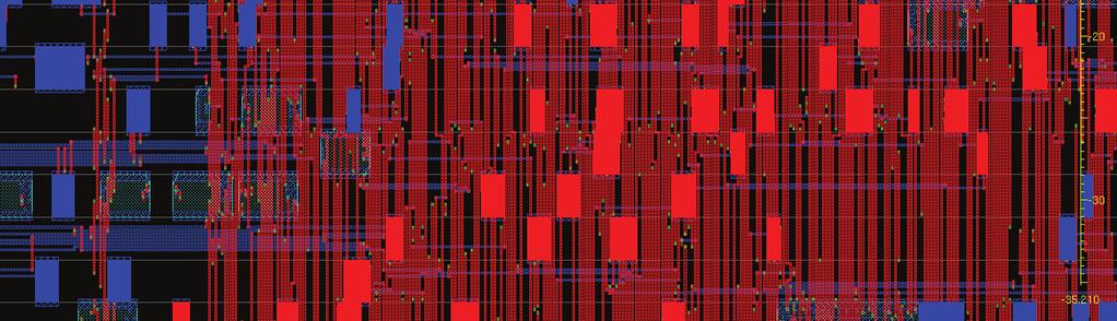
14 Floorplan Size of chip Location of Pins Location of main blocks Power supply: give enough power for each gate Power supply (1.8V) 1.75v 1.7v (need another power) 1.65v current VDD (Metal) Gate 1 Gate 2 Gate 3 Gate 4 VSS Voltage drop equation: V2 = V1 I * R

15 Floorplan of a single processor Inst Mem Data Mem ALU MAC Control Clock InFIFO 0 InFIFO 0
16 Placement & in-placement optimization Placement: place the gates In-placement optimization Why: timing information difference between synthesis and layout (wire delay) How: change gate size, insert buffers Should not change the circuit function!!

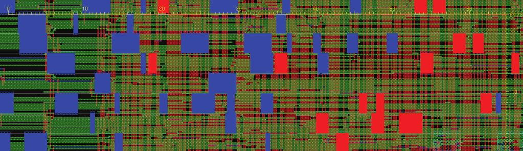
17 Placement of a single processor
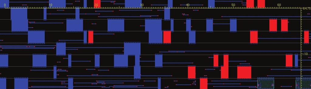
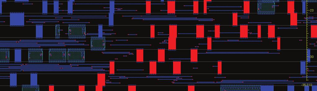
18 Clock tree Main parameters: skew, delay, transition time

19 Clock tree of single processor
20 Routing Connect the gates using wires Two steps Connect the global signals (power) Connect other signals


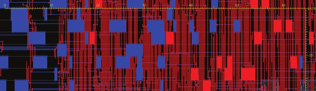
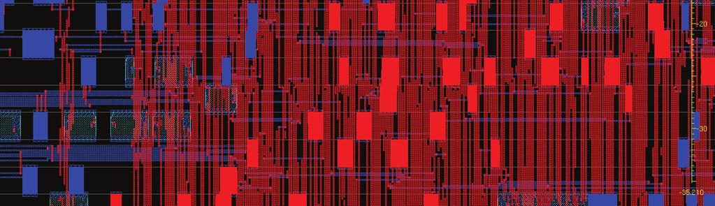
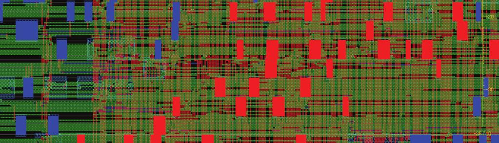
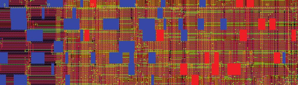
21 Metal Layer Topology Routing

22 Layout of a single processor Area: 0.8mm x 0.8mm Estimated speed: 450 MHz

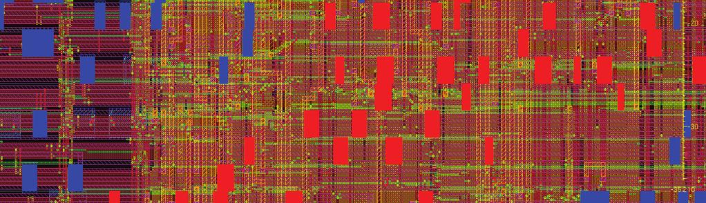
23 Layout of the first generation 6x6 AsAP Area: 30 mm^2 in 180 nm CMOS 36 processors 114 PADs One processor
24 Verification after layout DRC (design rule check) LVS (layout vs. schematic).gds vs. (verilog + spice module) Gate level verilog dynamic simulation Mainly check the function Different with synthesis result
25 Useful tools Dynamic Simulation: Modelsim (Mentor), NC-verilog (Cadence), Active-HDL Synthesis: Design-compiler, design-analyzer (Synopsys) Placement & Routing Encounter & icfb (Cadence) Astro (Synopsys) DRC & LVS Calibre (Mentor) Dracula (Cadence) Static Analysis Primetime (Synsopsys)
An Overview of Standard Cell Based Digital VLSI Design
 An Overview of Standard Cell Based Digital VLSI Design With examples taken from the implementation of the 36-core AsAP1 chip and the 1000-core KiloCore chip Zhiyi Yu, Tinoosh Mohsenin, Aaron Stillmaker,
Implementing Tile-based Chip Multiprocessors with GALS Clocking Styles
 Implementing Tile-based Chip Multiprocessors with GALS Clocking Styles Zhiyi Yu, Bevan Baas VLSI Computation Lab, ECE Department University of California, Davis, USA Outline Introduction Timing issues
Cell-Based IC Physical Design & Verification SOC Encounter. Advisor : 李昆忠 Presenter : 蕭智元
 Cell-Based IC Physical Design & Verification SOC Encounter Advisor : 李昆忠 Presenter : 蕭智元 Reference: SOC Encounter Training Manual, 2007, edited by CIC. Introduction We ll use some EDA tools to transform
ASIC Physical Design Top-Level Chip Layout
 ASIC Physical Design Top-Level Chip Layout References: M. Smith, Application Specific Integrated Circuits, Chap. 16 Cadence Virtuoso User Manual Top-level IC design process Typically done before individual
The Design of the KiloCore Chip
 The Design of the KiloCore Chip Aaron Stillmaker*, Brent Bohnenstiehl, Bevan Baas DAC 2017: Design Challenges of New Processor Architectures University of California, Davis VLSI Computation Laboratory
FABRICATION TECHNOLOGIES
 FABRICATION TECHNOLOGIES DSP Processor Design Approaches Full custom Standard cell** higher performance lower energy (power) lower per-part cost Gate array* FPGA* Programmable DSP Programmable general
The IIT standard cell library Version 2.1
 The IIT standard cell library Version 2.1 Highlights - Support for AMI 0.35um library, including pads - Added Primetime and Pathmill support to IIT ASIC Flow - Support for stacked vias (for Virtuoso and
Lab. Course Goals. Topics. What is VLSI design? What is an integrated circuit? VLSI Design Cycle. VLSI Design Automation
 Course Goals Lab Understand key components in VLSI designs Become familiar with design tools (Cadence) Understand design flows Understand behavioral, structural, and physical specifications Be able to
Logic Synthesis. Logic Synthesis. Gate-Level Optimization. Logic Synthesis Flow. Logic Synthesis. = Translation+ Optimization+ Mapping
 Logic Synthesis Logic Synthesis = Translation+ Optimization+ Mapping Logic Synthesis 2 Gate-Level Optimization Logic Synthesis Flow 3 4 Design Compiler Procedure Logic Synthesis Input/Output 5 6 Design
Synthesizable FPGA Fabrics Targetable by the VTR CAD Tool
 Synthesizable FPGA Fabrics Targetable by the VTR CAD Tool Jin Hee Kim and Jason Anderson FPL 2015 London, UK September 3, 2015 2 Motivation for Synthesizable FPGA Trend towards ASIC design flow Design
Cell-Based Design Flow. TA : 吳廸優
 Cell-Based Design Flow TA : 吳廸優 dywu@viplab.cs.nctu.edu.tw 1 Outline Overview Design Flow Stage 1 RTL Development Synthesis Gate Level Simulation Design Flow Stage 2 Placement and Routing Post Layout Simulation
Silicon Virtual Prototyping: The New Cockpit for Nanometer Chip Design
 Silicon Virtual Prototyping: The New Cockpit for Nanometer Chip Design Wei-Jin Dai, Dennis Huang, Chin-Chih Chang, Michel Courtoy Cadence Design Systems, Inc. Abstract A design methodology for the implementation
DIGITAL SANDBOX WORKSHOP Summer Digital Sandbox Mission
 DIGITAL SANDBOX WORKSHOP Summer 2004 Sandbox CAD Support Digital Sandbox Mission The virtual SoC design support facility provides "industrial strength" hardware, software, EDA tools, workflows, and technical
EECS 627, Lab Assignment 3
 EECS 627, Lab Assignment 3 1 Introduction In this lab assignment, we will use Cadence ICFB and Calibre to become familiar with the process of DRC/LVS checks on a design. So far, we have placed and routed
Laboratory 6. - Using Encounter for Automatic Place and Route. By Mulong Li, 2013
 CME 342 (VLSI Circuit Design) Laboratory 6 - Using Encounter for Automatic Place and Route By Mulong Li, 2013 Reference: Digital VLSI Chip Design with Cadence and Synopsys CAD Tools, Erik Brunvand Background
The Microprocessor as a Microcosm:
 The Microprocessor as a Microcosm: A Hands-On Approach to VLSI Design Education David Harris David_Harris@hmc.edu November 2002 Harvey Mudd College Claremont, CA Outline Introduction Course Organization
EE 330 Laboratory Experiment Number 11
 EE 330 Laboratory Experiment Number 11 Design and Simulation of Digital Circuits using Hardware Description Languages Fall 2017 Contents Purpose:... 3 Background... 3 Part 1: Inverter... 4 1.1 Simulating
ESE 570 Cadence Lab Assignment 2: Introduction to Spectre, Manual Layout Drawing and Post Layout Simulation (PLS)
") ESE 570 Cadence Lab Assignment 2: Introduction to Spectre, Manual Layout Drawing and Post Layout Simulation (PLS) Objective Part A: To become acquainted with Spectre (or HSpice) by simulating an inverter,
ESE 570 Cadence Lab Assignment 2: Introduction to Spectre, Manual Layout Drawing and Post Layout Simulation (PLS) Objective Part A: To become acquainted with Spectre (or HSpice) by simulating an inverter,
UNIVERSITY OF WATERLOO
 UNIVERSITY OF WATERLOO UW ASIC DESIGN TEAM: Cadence Tutorial Description: Part I: Layout & DRC of a CMOS inverter. Part II: Extraction & LVS of a CMOS inverter. Part III: Post-Layout Simulation. The Cadence
Outline. SoC Encounter Flow. Typical Backend Design Flow. Digital IC-Project and Verification. Place and Route. Backend ASIC Design flow
 Outline Digital IC-Project and Verification Deepak Dasalukunte Backend ASIC Design flow General steps Input files Floorplanning Placement Clock-synthesis Routing Typical Backend Design Flow SoC Encounter
Overview of Digital Design Methodologies
 Overview of Digital Design Methodologies ELEC 5402 Pavan Gunupudi Dept. of Electronics, Carleton University January 5, 2012 1 / 13 Introduction 2 / 13 Introduction Driving Areas: Smart phones, mobile devices,
An Asynchronous Array of Simple Processors for DSP Applications
 An Asynchronous Array of Simple Processors for DSP Applications Zhiyi Yu, Michael Meeuwsen, Ryan Apperson, Omar Sattari, Michael Lai, Jeremy Webb, Eric Work, Tinoosh Mohsenin, Mandeep Singh, Bevan Baas
Cadence On-Line Document
 Cadence On-Line Document 1 Purpose: Use Cadence On-Line Document to look up command/syntax in SoC Encounter. 2 Cadence On-Line Document An on-line searching system which can be used to inquire about LEF/DEF
Evolution of CAD Tools & Verilog HDL Definition
 Evolution of CAD Tools & Verilog HDL Definition K.Sivasankaran Assistant Professor (Senior) VLSI Division School of Electronics Engineering VIT University Outline Evolution of CAD Different CAD Tools for
TUTORIAL II ECE 555 / 755 Updated on September 11 th 2006 CADENCE LAYOUT AND PARASITIC EXTRACTION
 TUTORIAL II ECE 555 / 755 Updated on September 11 th 2006 CADENCE LAYOUT AND PARASITIC EXTRACTION After finishing a schematic of your design (Tutorial-I), the next step is creating masks which are for
Synthesis and APR Tools Tutorial
 Synthesis and APR Tools Tutorial (Last updated: Oct. 26, 2008) Introduction This tutorial will get you familiarized with the design flow of synthesizing and place and routing a Verilog module. All the
CPE/EE 427, CPE 527, VLSI Design I: Tutorial #4, Standard cell design flow (from verilog to layout, 8-bit accumulator)
") CPE/EE 427, CPE 527, VLSI Design I: Tutorial #4, Standard cell design flow (from verilog to layout, 8-bit accumulator) Joel Wilder, Aleksandar Milenkovic, ECE Dept., The University of Alabama in Huntsville
CPE/EE 427, CPE 527, VLSI Design I: Tutorial #4, Standard cell design flow (from verilog to layout, 8-bit accumulator) Joel Wilder, Aleksandar Milenkovic, ECE Dept., The University of Alabama in Huntsville
SYNTHESIS FOR ADVANCED NODES
 SYNTHESIS FOR ADVANCED NODES Abhijeet Chakraborty Janet Olson SYNOPSYS, INC ISPD 2012 Synopsys 2012 1 ISPD 2012 Outline Logic Synthesis Evolution Technology and Market Trends The Interconnect Challenge
Brief Introduction of Cell-based Design. Ching-Da Chan CIC/DSD
 Brief Introduction of Cell-based Design Ching-Da Chan CIC/DSD 1 Design Abstraction Levels SYSTEM MODULE + GATE CIRCUIT S n+ G DEVICE n+ D 2 Full Custom V.S Cell based Design Full custom design Better patent
Improved Circuit Reliability/Robustness. Carey Robertson Product Marketing Director Mentor Graphics Corporation
 Improved Circuit Reliability/Robustness Carey Robertson Product Marketing Director Mentor Graphics Corporation Reliability Requirements are Growing in all Market Segments Transportation Mobile / Wireless
23. Digital Baseband Design
 23. Digital Baseband Design Algorithm-to-VLSI Circuit Refinement (Floating Point) Tradeoff (SNR Loss, BER) (Fixed Point) VHDL, Verilog VHDL, Verilog Memory Control For I=0 to I=15 Sum = Sum + array[i]
EE 330 Laboratory Experiment Number 11 Design, Simulation and Layout of Digital Circuits using Hardware Description Languages
 EE 330 Laboratory Experiment Number 11 Design, Simulation and Layout of Digital Circuits using Hardware Description Languages Purpose: The purpose of this experiment is to develop methods for using Hardware
Linking Layout to Logic Synthesis: A Unification-Based Approach
 Linking Layout to Logic Synthesis: A Unification-Based Approach Massoud Pedram Department of EE-Systems University of Southern California Los Angeles, CA February 1998 Outline Introduction Technology and
CMOS VLSI Design Lab 3: Controller Design and Verification
 CMOS VLSI Design Lab 3: Controller Design and Verification The controller for your MIPS processor is responsible for generating the signals to the datapath to fetch and execute each instruction. It lacks
Cell-Based Design Flow. 林丞蔚
 Cell-Based Design Flow 林丞蔚 cultom@viplab.cs.nctu.edu.tw 1 Outline Overview Design Flow 1 RTL Development Synthesis Gate Level Simulation Design Flow 2 Placement and Routing Example Design IC Contest 2006
CMOS VLSI Design Lab 3: Controller Design and Verification
 CMOS VLSI Design Lab 3: Controller Design and Verification The controller for your MIPS processor is responsible for generating the signals to the datapath to fetch and execute each instruction. It lacks
MOSAID Semiconductor
 MOSAID Semiconductor Fabr-IC (A Single-Chip Gigabit Ethernet Switch With Integrated Memory) @Hot Chips Dave Brown Chief Architect July 4, 2001 Fabr-IC Feature summary 2 Gig ports 1 gig port for stacking
ECE 459/559 Secure & Trustworthy Computer Hardware Design
 ECE 459/559 Secure & Trustworthy Computer Hardware Design VLSI Design Basics Garrett S. Rose Spring 2016 Recap Brief overview of VHDL Behavioral VHDL Structural VHDL Simple examples with VHDL Some VHDL
CMOS VLSI Design Lab 3: Controller Design and Verification
 CMOS VLSI Design Lab 3: Controller Design and Verification The controller for your MIPS processor is responsible for generating the signals to the datapath to fetch and execute each instruction. It lacks
Digital IC- Project 1. Place and Route. Oskar Andersson. Oskar Andersson, EIT, LTH, Digital IC project and Verifica=on
 Digital IC- Project 1 Oskar Andersson Outline Backend ASIC Design flow (Physical Design) General steps Input files Floorplanning Placement ClockTree- synthesis Rou=ng Typical Backend Design Flow Synthesis
ProASIC PLUS FPGA Family
 ProASIC PLUS FPGA Family Key Features Reprogrammable /Nonvolatile Flash Technology Low Power Secure Single Chip/Live at Power Up 1M Equivalent System Gates Cost Effective ASIC Alternative ASIC Design Flow
Digital System Design Lecture 2: Design. Amir Masoud Gharehbaghi
 Digital System Design Lecture 2: Design Amir Masoud Gharehbaghi amgh@mehr.sharif.edu Table of Contents Design Methodologies Overview of IC Design Flow Hardware Description Languages Brief History of HDLs
Lecture 11 Logic Synthesis, Part 2
 Lecture 11 Logic Synthesis, Part 2 Xuan Silvia Zhang Washington University in St. Louis http://classes.engineering.wustl.edu/ese461/ Write Synthesizable Code Use meaningful names for signals and variables
EE 330 Laboratory Experiment Number 11 Design and Simulation of Digital Circuits using Hardware Description Languages
 EE 330 Laboratory Experiment Number 11 Design and Simulation of Digital Circuits using Hardware Description Languages Fall 2015 Purpose: The purpose of this experiment is to develop methods for using Hardware
Serial Adapter for I 2 C / APFEL and 8 channel DAC ASIC
 Serial Adapter for I 2 C / APFEL and 8 channel DAC ASIC GSI Helmholtzzentrum für Schwerionenforschung GmbH Experiment Electronics Department December 5, 2016 Outline 1 Motivation 2 3 Motivation Currently
Tutorial for Cadence SOC Encounter Place & Route
 Tutorial for Cadence SOC Encounter Place & Route For Encounter RTL-to-GDSII System 13.15 T. Manikas, Southern Methodist University, 3/9/15 Contents 1 Preliminary Setup... 1 1.1 Helpful Hints... 1 2 Starting
Design Solutions in Foundry Environment. by Michael Rubin Agilent Technologies
 Design Solutions in Foundry Environment by Michael Rubin Agilent Technologies Presenter: Michael Rubin RFIC Engineer, R&D, Agilent Technologies former EDA Engineering Manager Agilent assignee at Chartered
A 167-processor Computational Array for Highly-Efficient DSP and Embedded Application Processing
 A 167-processor Computational Array for Highly-Efficient DSP and Embedded Application Processing Dean Truong, Wayne Cheng, Tinoosh Mohsenin, Zhiyi Yu, Toney Jacobson, Gouri Landge, Michael Meeuwsen, Christine
TSBCD025 High Voltage 0.25 mm BCDMOS
 TSBCD025 High Voltage 0.25 mm BCDMOS TSI Semiconductors' 0.25 mm process is a feature rich platform with best in class CMOS, LDMOS, and BiPolar devices. The BCD technology enables logic, Mixed-Signal,
Processor Architectures At A Glance: M.I.T. Raw vs. UC Davis AsAP
 Processor Architectures At A Glance: M.I.T. Raw vs. UC Davis AsAP Presenter: Course: EEC 289Q: Reconfigurable Computing Course Instructor: Professor Soheil Ghiasi Outline Overview of M.I.T. Raw processor
Hardware and Applications of AsAP: An Asynchronous Array of Simple Processors
 Hardware and Applications of AsAP: An Asynchronous Array of Simple Processors Bevan Baas, Zhiyi Yu, Michael Meeuwsen, Omar Sattari, Ryan Apperson, Eric Work, Jeremy Webb, Michael Lai, Daniel Gurman, Chi
Design of a Low Density Parity Check Iterative Decoder
 1 Design of a Low Density Parity Check Iterative Decoder Jean Nguyen, Computer Engineer, University of Wisconsin Madison Dr. Borivoje Nikolic, Faculty Advisor, Electrical Engineer, University of California,
ANALOG MICROELECTRONICS ( A)
") ANALOG MICROELECTRONICS (304-534A) IBM 130 nm CMOS Technology An Introduction to Cadence Virtuoso Layout Tool and the Analog Simulation Environment Prepared By - Azhar A. Chowdhury Updated by Ming Yang
ANALOG MICROELECTRONICS (304-534A) IBM 130 nm CMOS Technology An Introduction to Cadence Virtuoso Layout Tool and the Analog Simulation Environment Prepared By - Azhar A. Chowdhury Updated by Ming Yang
KiloCore: A 32 nm 1000-Processor Array
 KiloCore: A 32 nm 1000-Processor Array Brent Bohnenstiehl, Aaron Stillmaker, Jon Pimentel, Timothy Andreas, Bin Liu, Anh Tran, Emmanuel Adeagbo, Bevan Baas University of California, Davis VLSI Computation
Part B. Dengxue Yan Washington University in St. Louis
 Tools Tutorials Part B Dengxue Yan Washington University in St. Louis Tools mainly used in this class Synopsys VCS Simulation Synopsys Design Compiler Generate gate-level netlist Cadence Encounter placing
EECE 285 VLSI Design. Cadence Tutorial EECE 285 VLSI. By: Kevin Dick Co-author: Jeff Kauppila Co-author: Dr. Arthur Witulski
 Cadence Tutorial EECE 285 VLSI By: Kevin Dick Co-author: Jeff Kauppila Co-author: Dr. Arthur Witulski 1 Table of Contents Purpose of Cadence 1) The Purpose of Cadence pg. 4 Linux 1) The Purpose of Linux
DESIGN STRATEGIES & TOOLS UTILIZED
 CHAPTER 7 DESIGN STRATEGIES & TOOLS UTILIZED 7-1. Field Programmable Gate Array The internal architecture of an FPGA consist of several uncommitted logic blocks in which the design is to be encoded. The
CMOS Design Lab Manual
 CMOS Design Lab Manual Developed By University Program Team CoreEl Technologies (I) Pvt. Ltd. 1 Objective Objective of this lab is to learn the Mentor Graphics HEP2 tools as well learn the flow of the
Bits and Pieces of CS250 s Toolflow
 Bits and Pieces of CS250 s Toolflow CS250 Tutorial 2 (Version 092509a) September 25, 2009 Yunsup Lee In this tutorial you will learn what each VLSI tools used in class are meant to do, how they flow, file
Graphics: Alexandra Nolte, Gesine Marwedel, Universität Dortmund. RTL Synthesis
 Graphics: Alexandra Nolte, Gesine Marwedel, 2003 Universität Dortmund RTL Synthesis Purpose of HDLs Purpose of Hardware Description Languages: Capture design in Register Transfer Language form i.e. All
AMchip architecture & design
 Sezione di Milano AMchip architecture & design Alberto Stabile - INFN Milano AMchip theoretical principle Associative Memory chip: AMchip Dedicated VLSI device - maximum parallelism Each pattern with private
Hardware Modeling. Hardware Description. ECS Group, TU Wien
 Hardware Modeling Hardware Description ECS Group, TU Wien Content of this course Hardware Specification Functional specification High Level Requirements Detailed Design Description Realisation Hardware
Abstract Editor (Last updated: Oct. 23, 2008)
") Abstract Editor (Last updated: Oct. 23, 2008) Abstract Editor Tutorial This tutorial has been created to discuss all of the steps needed to create an abstract Library Exchange Format (LEF) file for custom
Abstract Editor (Last updated: Oct. 23, 2008) Abstract Editor Tutorial This tutorial has been created to discuss all of the steps needed to create an abstract Library Exchange Format (LEF) file for custom
PG Certificate. VLSI Design & Verification (RTL using Verilog, FPGA Design Flow & Verification) (Live Project)
 (Live Project)") PG Certificate in VLSI Design & Verification (RTL using Verilog, FPGA Design Flow & Verification) (Live Project) Certificates by National Skill Development Corporation (NSDC), Ministry of Skill Development
PG Certificate in VLSI Design & Verification (RTL using Verilog, FPGA Design Flow & Verification) (Live Project) Certificates by National Skill Development Corporation (NSDC), Ministry of Skill Development
Tutorial for Encounter
 Tutorial for Encounter STEP 1: Login to the Linux system on Linuxlab server. Start a terminal (the shell prompt). (If you don t know how to login to Linuxlab server, look at here) Click here to open a
EE 330 Spring Laboratory 2: Basic Boolean Circuits
 EE 330 Spring 2013 Laboratory 2: Basic Boolean Circuits Objective: The objective of this experiment is to investigate methods for evaluating the performance of Boolean circuits. Emphasis will be placed
ECE425: Introduction to VLSI System Design Machine Problem 3 Due: 11:59pm Friday, Dec. 15 th 2017
 ECE425: Introduction to VLSI System Design Machine Problem 3 Due: 11:59pm Friday, Dec. 15 th 2017 In this MP, you will use automated tools to synthesize the controller module from your MP2 project into
101-1 Under-Graduate Project Digital IC Design Flow
 101-1 Under-Graduate Project Digital IC Design Flow Speaker: Ming-Chun Hsiao Adviser: Prof. An-Yeu Wu Date: 2012/9/25 ACCESS IC LAB Outline Introduction to Integrated Circuit IC Design Flow Verilog HDL
Bits and Pieces of CS250 s Toolflow
 Bits and Pieces of CS250 s Toolflow CS250 Tutorial 2 (Version 091210a) September 12, 2010 Yunsup Lee In this tutorial you will learn what each VLSI tools used in class are meant to do, how they flow, file
EE 4755 Digital Design Using Hardware Description Languages
 EE 4755 Digital Design Using Hardware Description Languages Basic Information URL: http://www.ece.lsu.edu/v Offered by: David M. Koppelman, Room 345 ERAD Building 578-5482. koppel@ece.lsu.edu, http://www.ece.lsu.edu/koppel/koppel.html
A Hexagonal Shaped Processor and Interconnect Topology for Tightly-tiled Many-Core Architecture
 A Hexagonal Shaped Processor and Interconnect Topology for Tightly-tiled Many-Core Architecture Zhibin Xiao and Bevan Baas Department of Electrical and Computer Engineering, University of California, Davis
Physical Placement with Cadence SoCEncounter 7.1
 Physical Placement with Cadence SoCEncounter 7.1 Joachim Rodrigues Department of Electrical and Information Technology Lund University Lund, Sweden November 2008 Address for correspondence: Joachim Rodrigues
Physical Synthesis and Electrical Characterization of the IP-Core of an IEEE-754 Compliant Single Precision Floating Point Unit
 Physical Synthesis and Electrical Characterization of the IP-Core of an IEEE-754 Compliant Single Precision Floating Point Unit Alian Engroff, Leonardo Tomazine Neto, Edson Schlosser and Alessandro Girardi
Cadence Tutorial A: Schematic Entry and Functional Simulation Created for the MSU VLSI program by Andrew Mason and the AMSaC lab group.
 Cadence Tutorial A: Schematic Entry and Functional Simulation Created for the MSU VLSI program by Andrew Mason and the AMSaC lab group. Revision Notes: Aug. 2003 update and edit A. Mason add intro/revision/contents
Introduction to laboratory exercises in Digital IC Design.
 Introduction to laboratory exercises in Digital IC Design. A digital ASIC typically consists of four parts: Controller, datapath, memory, and I/O. The digital ASIC below, which is an FFT/IFFT co-processor,
Spiral 2-8. Cell Layout
 2-8.1 Spiral 2-8 Cell Layout 2-8.2 Learning Outcomes I understand how a digital circuit is composed of layers of materials forming transistors and wires I understand how each layer is expressed as geometric
Design and Analysis of Ultra Low Power Processors Using Sub/Near-Threshold 3D Stacked ICs
 Design and Analysis of Ultra Low Power Processors Using Sub/Near-Threshold 3D Stacked ICs Sandeep Kumar Samal, Yarui Peng, Yang Zhang, and Sung Kyu Lim School of ECE, Georgia Institute of Technology, Atlanta,
Circuit Design and Simulation with VHDL 2nd edition Volnei A. Pedroni MIT Press, 2010 Book web:
 Circuit Design and Simulation with VHDL 2nd edition Volnei A. Pedroni MIT Press, 2010 Book web: www.vhdl.us Appendix C Xilinx ISE Tutorial (ISE 11.1) This tutorial is based on ISE 11.1 WebPack (free at
FPGA Implementation and Validation of the Asynchronous Array of simple Processors
 FPGA Implementation and Validation of the Asynchronous Array of simple Processors Jeremy W. Webb VLSI Computation Laboratory Department of ECE University of California, Davis One Shields Avenue Davis,
VLSI Design Automation
 VLSI Design Automation IC Products Processors CPU, DSP, Controllers Memory chips RAM, ROM, EEPROM Analog Mobile communication, audio/video processing Programmable PLA, FPGA Embedded systems Used in cars,
DIGITAL DESIGN TECHNOLOGY & TECHNIQUES
 DIGITAL DESIGN TECHNOLOGY & TECHNIQUES CAD for ASIC Design 1 INTEGRATED CIRCUITS (IC) An integrated circuit (IC) consists complex electronic circuitries and their interconnections. William Shockley et
A 167-processor 65 nm Computational Platform with Per-Processor Dynamic Supply Voltage and Dynamic Clock Frequency Scaling
 A 167-processor 65 nm Computational Platform with Per-Processor Dynamic Supply Voltage and Dynamic Clock Frequency Scaling Dean Truong, Wayne Cheng, Tinoosh Mohsenin, Zhiyi Yu, Toney Jacobson, Gouri Landge,
 DEPT OF ECE EC6612 -VLSI DESIGN LABORATORY MANUAL (REGULATION-2013) LAB MANUAL DEPARTMENT OF ECE NAME: REGISTER NUMBER: YEAR/SEM.: ACADEMIC YEAR: 2015-2016 DEPT OF ECE EC6612 -VLSI DESIGN LABORATORY MANUAL
RISECREEK: From RISC-V Spec to 22FFL Silicon
 RISECREEK: From RISC-V Spec to 22FFL Silicon Vinod Ganesan, Gopinathan Muthuswamy Group CSE Dept RISE Lab IIT Madras Amudhan, Bharath, Alagu - HCL Tech Konala Varma, Ang Boon Chong, Harish Villuri - Intel
Introduction to CMOS VLSI Design (E158) Project 2 Spring 2008
 Project 2 Spring 2008") Harris Introduction to CMOS VLSI Design (E158) Project 2 Spring 2008 The E158 class will all collaborate to build a 6502 microprocessor optimized for minimum power at 1 MHz operation. The processor will
Harris Introduction to CMOS VLSI Design (E158) Project 2 Spring 2008 The E158 class will all collaborate to build a 6502 microprocessor optimized for minimum power at 1 MHz operation. The processor will
TABLE OF CONTENTS 1.0 PURPOSE INTRODUCTION ESD CHECKS THROUGHOUT IC DESIGN FLOW... 2
 TABLE OF CONTENTS 1.0 PURPOSE... 1 2.0 INTRODUCTION... 1 3.0 ESD CHECKS THROUGHOUT IC DESIGN FLOW... 2 3.1 PRODUCT DEFINITION PHASE... 3 3.2 CHIP ARCHITECTURE PHASE... 4 3.3 MODULE AND FULL IC DESIGN PHASE...
A Non-Volatile Microcontroller with Integrated Floating-Gate Transistors
 A Non-Volatile Microcontroller with Integrated Floating-Gate Transistors Wing-kei Yu, Shantanu Rajwade, Sung-En Wang, Bob Lian, G. Edward Suh, Edwin Kan Cornell University 2 of 32 Self-Powered Devices
Floorplan and Power/Ground Network Co-Synthesis for Fast Design Convergence
 Floorplan and Power/Ground Network Co-Synthesis for Fast Design Convergence Chen-Wei Liu 12 and Yao-Wen Chang 2 1 Synopsys Taiwan Limited 2 Department of Electrical Engineering National Taiwan University,
310/ ICTP-INFN Advanced Tranining Course on FPGA and VHDL for Hardware Simulation and Synthesis 27 November - 22 December 2006
 310/1780-18 ICTP-INFN Advanced Tranining Course on FPGA and VHDL for Hardware Simulation and Synthesis 27 November - 22 December 2006 Design Methodology Tools Jorgen CHRISTIANSEN PH-ED CERN CH-1221 Geneva
VLSI Design Automation
 VLSI Design Automation IC Products Processors CPU, DSP, Controllers Memory chips RAM, ROM, EEPROM Analog Mobile communication, audio/video processing Programmable PLA, FPGA Embedded systems Used in cars,
RTL Coding General Concepts
 RTL Coding General Concepts Typical Digital System 2 Components of a Digital System Printed circuit board (PCB) Embedded d software microprocessor microcontroller digital signal processor (DSP) ASIC Programmable
Synopsys Design Platform
 Synopsys Design Platform Silicon Proven for FDSOI Swami Venkat, Senior Director, Marketing, Design Group September 26, 2017 2017 Synopsys, Inc. 1 Synopsys: Silicon to Software Software Application security
Batch Processing: The Complete Synthesize, Place, and Route Flow
 Batch Processing: The Complete Synthesize, Place, and Route Flow Daniel Liu, John Lee, Puneet Gupta University of California, Los Angeles, NanoCAD Lab {daniel,lee,puneet}@ee.ucla.edu Abstract Design automation
CMOS VLSI Design. Final Project
 Harris CMOS VLSI Design Final Project 1. Overview The final project is a chance for you to apply your new skills in VLSI design to a moderate sized problem of your choosing as part of a two-person team.
An Interconnect-Centric Design Flow for Nanometer Technologies
 An Interconnect-Centric Design Flow for Nanometer Technologies Jason Cong UCLA Computer Science Department Email: cong@cs.ucla.edu Tel: 310-206-2775 URL: http://cadlab.cs.ucla.edu/~cong Exponential Device
CMOS VLSI Design Lab 2: Datapath Design and Verification
 CMOS VLSI Design Lab 2: Datapath Design and Verification In this lab, you will begin designing an 8-bit MIPS processor. You will first review and simulate a Verilog model of the overall processor. You
VLSI Design Automation. Calcolatori Elettronici Ing. Informatica
 VLSI Design Automation 1 Outline Technology trends VLSI Design flow (an overview) 2 IC Products Processors CPU, DSP, Controllers Memory chips RAM, ROM, EEPROM Analog Mobile communication, audio/video processing
Overview. Design flow. Principles of logic synthesis. Logic Synthesis with the common tools. Conclusions
 Logic Synthesis Overview Design flow Principles of logic synthesis Logic Synthesis with the common tools Conclusions 2 System Design Flow Electronic System Level (ESL) flow System C TLM, Verification,
A Design Tradeoff Study with Monolithic 3D Integration
 A Design Tradeoff Study with Monolithic 3D Integration Chang Liu and Sung Kyu Lim Georgia Institute of Techonology Atlanta, Georgia, 3332 Phone: (44) 894-315, Fax: (44) 385-1746 Abstract This paper studies
Interconnect Delay Aware RTL Verilog Bus Architecture Generation for an SoC
 Interconnect Delay Aware RTL Verilog Bus Architecture Generation for an SoC Kyeong Ryu, Alexandru Talpasanu, Vincent Mooney and Jeffrey Davis School of Electrical and Computer Engineering Georgia Institute