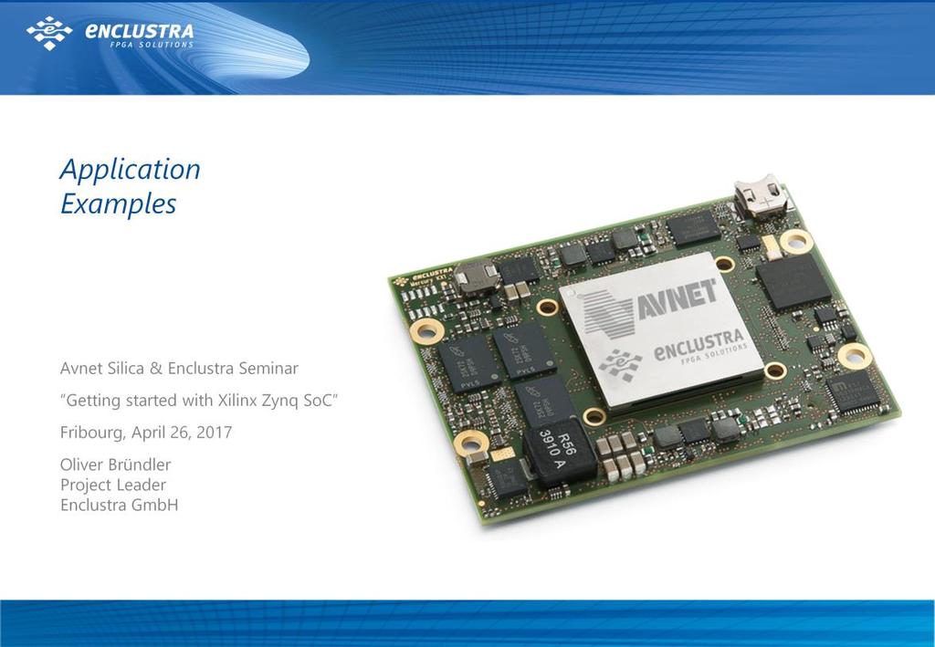
Application Examples Avnet Silica & Enclustra Seminar Getting started with Xilinx Zynq SoC Fribourg, April 26, 2017
|
|
|
- Junior Johns
- 6 years ago
- Views:
Transcription
1 1
2 2

3 3 Introduction The next few slides give a brief overview of what will be discussed in this presentation and they contain some general points that apply to both examples covered. The presentation does not only highlight the implementation of the projects discussed but it points out as well what know-how is required to successfully realize an offloading engine using FPGA fabric within an SoC.

4 4 Projects Discussed Two very different projects are discussed in this presentation. The first project is a statistical image processing engine whose only purpose is to accelerate an algorithm already implemented in software. Since the customer is doing statistical image processing regularly, the engine has to be designed in a reusable way. The algorithms to speed up were known when the project started, so the operations to implement were specified exactly and Enclustra was only responsible for converting the operations into a form that can be implemented in SoC fabric easily (fixed-point-quantization, approximations, etc.). The second project is a Bluetooth transceiver. It allows receiving and transmitting packets. All link-layer operations (data encoding, header generation, etc.) and physical-layer operations (modulation, demodulation, filtering, etc.) are executed within the offloading engine. The algorithms were developed by Enclustra since the customer has a lot of knowledge in protocol handling but less knowledge in digital signal processing. Because the requirements are very project specific, the transceiver is not optimized for reusage. There is one point both example projects have in common: They are both fixed-point math intensive.
 is prone to misunderstandings.")
5 5 Enclustra Fixed-Point Math Development Flow To understand the examples discussed in this presentation, a basic knowledge about the development flow used for both projects is required. Therefore this flow is described briefly. Almost every engineer made the experience that written language (or even worse: spoken language) is prone to misunderstandings. Moreover language does not enforce the specification of all corner cases, which leads to unclear requirements. Nevertheless, written language is used for most specifications. This introduces significant risk for both sides, the customer (delay) and Enclustra as service company (rework effort). In some cases, customers are already aware of these problems and provide a MATLAB, Simulink or C implementation of the algorithm to be implemented in an FPGA or SoC. Even though this solves the problem of misunderstandings regarding the specification, the algorithms provided are often using double precision floating point numbers which are not implementable efficiently in FPGA fabric. As a result the algorithm must be changed to work with fixed-point operations and other implementation-optimized concepts such as taylor approximations for functions. This conversion leads to slight changes in the behavior and therefore again to the risk that the algorithm does not perform as expected and rework is required. To reduce the risk described above, Enclustra always implements a fixed-point model of the algorithm in such a way that it can be implemented bit-true in the FPGA fabric. The customer can then analyze the performance of the algorithm and identify changes required to meet all requirements before the implementation is started. After approval by the customer, the bittrue model of the algorithm is used as specification for the implementation. This approach significantly reduces risk for both sides and improves work efficiency since a 100% clear an implementable specification in a programming language (usually MATLAB) exists when the implementation of the offloading engine is started.

6 6 bit-true Co-Simulations The central point of the development flow described on the last slide is to ensure that the FPGA fabric implementation is bit-true to the MATLAB model approved by the customer. Since this is crucial to all algorithm related projects Enclustra works on, some libraries were developed to increase the efficiency in doing so. One library contains bit-true implementation of common functions for MATLAB, VHDL and C. It includes basic operations such as addition or multiplication as well as more complex building blocks such as taylor approximations or CORDIC. If this library is used for all operations in the MATLAB model of the algorithm, it is implicitly bit-true implementable in VHDL. The second important library contains functions to read and write files containing stimuli and responses from MATLAB and VHDL. This library is used to communicate between the MATLAB part and the VHDL part of a co-simulation. Co-simulations are implemented for each VHDL entity and always consist of a MATLAB and a VHDL part. The MATLAB part of the co-simulation generates stimuli and feeds them into the bit-true model of the entity under test. Stimuli as well as response of the model are written to files using the library described above. The VHDL simulation reads the stimuli from this file, applies them to the VHDL implementation of the entity under test and automatically checks if the response matches the expectation. If the responses do not exactly (bit by bit) match, errors are written into a report file. Additionally the actual response of the VHDL implementation is written into a file. This file can be read from MATLAB and analyzed, which is very helpful for finding the root-cause of any mismatches.
7 7 Statistical Image Processing Engine The next few slides describe the implementation of a statistical image processing acceleration engine. The goal is not to exactly describe the engine discussed but to pick out some interesting points.

8 8 Target Algorithm Even though the image processing engine discussed was implemented in a reusable way, one target algorithm and therefore an exact set of operations was already known when the project started. Only a few of the operations are straight forward implementable in FPGA fabric: Addition Subtraction Multiplication Per image operations The other operations made high demands on design to achieve an efficient implementation in FPGA fabric: Division and Squareroot are implemented using taylor approximations and shift operations Complex operations are implemented using CORDIC Multi image operations require reading and buffering up to 32 images in parallel even though all other operations require only 2 input images The region of interest (ROI) for the images to be processed must be configurable at runtime.

9 9 Goals and Achievements The algorithm to be accelerated was already implemented on the Cortex-A9 processor available in Zynq SoCs running at 600 MHz. The main goal of the customer was to reduce the execution time for the algorithm from around 60 seconds to around 5-10 seconds. This corresponds to a 6-12x speedup. CPU load should be reduced to allow other tasks such as communication running smoothly in the background. Thanks to offloading of all actual operations on images, the CPU load dropped dramatically. The image processing engine runs at 100 MHz and can process one pixel every clock cycle. This results in a full image operation execution time of around 1 ms and reduces the complete algorithm execution time to around 3 sec (including multi-image operations, control overhead and more complex operations still implemented in software), which corresponds to a speedup of 20x and therefore already exceeds the initial goals of the customer. Because of the nature of the target application, faster execution is beneficial even beyond the initial goals. Therefore the customer decided to use four accelerators in parallel (one for each of four parallel image streams) to further increase the speedup. This results in a breathtaking speedup of 80x compared to the existing implementation in software. As nice side effect, the power consumption of the system dropped. However, power consumption was not a main concern in this project.

10 10 General Architecture The image processing engine discussed consists of five main parts: Control logic Contains a register bank containing all settings (e.g. selection of operation, addresses of input and output images) Regularly issues read and write operations to make sure no overflows respectively underruns occur in the input/output buffers Notifies the CPU via IRQ when the operation is completed AXI4-master interface Reads input data and write output data directly from/to DDR memory Input buffer This is basically a multi-channel FIFO which buffers the input images Required because of the bursting nature of DDR memory accesses Output buffer The output image also needs to be buffered Required because of the bursting nature of DDR memory accesses Processing unit Executes the operation selected
 and because other components such as the CPU and other processing units are accessing the same DDR memory in parallel.")
11 11 Multi Channel Input Buffer The requirement for the input buffer is to contain enough data to keep the processing unit active while a DDR memory read access is issued but not yet completed. Unfortunately the response time of the DDR memory is strongly affected by jitter because of the nature of DDR memories in general (e.g. refresh cycles) and because other components such as the CPU and other processing units are accessing the same DDR memory in parallel. It was found that the buffer is required to contain enough data to keep the processing unit running for about 40 µs which corresponds to 4096 pixels (8 kb) per input for operations with one or two images. This results in a total of 8 BlockRAMs (2 kb each) required for the input buffer. This sounds reasonable at the first glance but there are these multi-image operations with up to 32 input images. If a 4096 pixel buffer was implemented for all 32 input images, a total of 256 kb buffer space would be required, which translates into 128 BlockRAMs. This is not reasonable to implement since the device targeted only contains 240 BlockRAMs and more than one engine needs to be implemented. Fortunately all up to 32 images are processed time interleaved (one pixel of every image one after the other, then the next pixel, etc.). As a result, the processing engine can be kept active for 40 µs not with 4096 pixels per image but with 4096 pixels in total. This results in the initially estimated 8 BlockRAMs being sufficient but now every image just gets less buffer space (128 pixels for 32 images, 256 pixels for 16 images, etc.).
 multiplication. This problem was solved by using a taylor approximation of the 1/x function together with a multiplication instead of implementing a binary divider.")
12 12 Division Implementation The first problem with divisions is that they cannot be implemented resource efficient in FPGA fabric in contrast to addition and subtraction as well as (thanks to embedded multipliers) multiplication. This problem was solved by using a taylor approximation of the 1/x function together with a multiplication instead of implementing a binary divider. The second problem is that the 1/x function doubles the number of bits required to represent the whole result range in appropriate precision. In our case this would lead to a taylor approximation with 32-bit output which is not reasonably implementable. To solve this problem, the operation was mathematically transformed into a form which only requires the taylor approximation to be valid in the range between 0.5 and 1. This comes at the cost of two shift operators which are easily implementable in FPGA fabric. In other words: Non technology friendly operations (division, full-range 1/x) were replaced by more technology friendly operations (multiplication, taylor approximation, shifts). This clearly shows that the efficient implementation of algorithms in FPGA fabric requires a lot of know-how about technology friendly implementation approaches, which will never be replaceable by tools. The implementation of the division also shows why the verification of a bit-true model of each operation by the customer is required: Even though the division of two 16-bit numbers with 32-bit result is mathematically 100% defined, the results of the implementation chosen may differ by a few LSBs. It is up to the customer to decide if this performance is sufficient or if a more precise implementation is required at the cost of more resources.
13 13 Bluetooth Transceiver Engine The next few slides describe the implementation of a Bluetooth transceiver engine. Again the goal is not to explain each and every detail but to select some interesting points and discuss them.

14 14 Requirements Let s first answer the most obvious question: Why is anybody using SoC technology for doing Bluetooth even though very cheap Bluetooth chips are available off-theshelf? The answer is that the target application is a Bluetooth qualification setup. This means that not only communication via Bluetooth is required but also very controlled signal generation including exact frequency offsets and other TX (transmit) defects. On the RX (receive) side some additional measurements are required too. Software defined radio (SDR) allows controlling all parameters of the signal processing exactly and changing them easily on the fly. SDR systems are not affected by temperature effects and aging since the signal processing is defined by algorithms and digitally stored parameters. As a result SDR is the ideal technology to fulfill the high requirements of this project and SoCs are the ideal platform to implement SDR thanks to the power of parallel processing. In parallel to the transceiver engine discussed, the qualification process involves RF measurements. This is another reason why using a standard Bluetooth chip is not an option. Note that the RF measurements are not included in the Bluetooth transceiver engine. The received signal is recorded in parallel to the transceiver engine responsible for communicating using the Bluetooth protocol.
 packet. It is modulated using GFSK, which is a type for frequency modulation. One bit is transferred with every symbol and the symbol rate is 1 MSPS.")
15 15 Bluetooth Protocol Basics To understand the following slides, it is important to know the basics of the Bluetooth low-level protocol. Therefore the protocol is presented in a simplified form. The most basic packet type is a basic rate (BR) packet. It is modulated using GFSK, which is a type for frequency modulation. One bit is transferred with every symbol and the symbol rate is 1 MSPS. To improve the data rate, enhanced data rate (EDR) packets come into play. The meta information is encoded equally to the BR packets but the data is encoded using DPSK, which is a type of phase modulation. Two (EDR2, 4-DPSK) or three (EDR3, 8- DPSK) bits are transferred with every symbol but the symbol rate is unchanged at 1 MSPS. To reduce power consumption, an additional packet type is defined: The low energy (BLE) packet. It uses the same modulation type as the BR packet but has a different packet structure and slightly different modulation parameters. For improved data rate at low power consumption, the BLE 2 Mbps packet type is used. It is equal to the BLE1 packet but the symbol rate is doubled to 2 MSPS. The packet types mentioned lead to the requirement for implementing three different modulation/demodulation schemes and two different symbol rates for GFSK. This is important to understand the general structure of the engine.

16 16 General Architecture To transmit a packet, the information about the packet including the payload data is writen into the packet generator via the AXI4-slave interface of the offloading engine. The packet generator then assembles the packet according to the protocol, calculates CRC checksums, does forward error coding, etc. The binary data is then modulated using the appropriate modulation scheme. A controlled symbol rate error can be introduced within the modulator, which requires a high precision resampling. For EDR packets, the first part of the packet is GFSK modulated while the payload is DPSK modulated. The fader is responsible for softly switching between the modulation schemes to avoid transmitting wideband noise du to hard transitions. The signal conditioning unit is used to add a well defined frequency offset and set a signal gain. The resampling and filtering unit changes the sampling rate from the internally used 8/16 MHz (16 MHz for BLE 2 Mbps, 8 MHz for all ohter packet types) to 2 MHz used by the RF frontend. If a packet is received, the operations are inverted. First the signal is converted to the internally used sample rate of 8/16 MHz. The demodulators then extract the binary data and the packet receiver detects packets and decodes them. The CPU is notified whenever a packet is received and can read the packet data via the AXI4-slave interface.
.")
17 17 Loopback Testing in Simulations and on Hardware To achieve a good test coverage and find all issues before delivering the offloading engine, a thorough testing concept was implemented additionally to the normal regression testing concept in use at Enclustra (self-checking regression tests). In simulations the whole processing chain was simulated in a loopback configuration (blue) for only a hand full of packets due to long simulation runtimes. Additionally several loopback paths are implemented and can be activated on hardware. This allows testing many thousands of packets within a short time. Thanks to multiple loopback paths (red), any problems can be roughly located very quickly which saves a lot of debugging time. Before delivering the Bluetooth transceiver engine to the cusomer, loopback tests for over a million packets were run including the RF frontend and the antenna. Thanks to the consideration of loopback tests early in the concept phase, care was taken to design the system symmetrically (e.g. same sample rates and number formats on RX and TX side) to ease the implementation of loopback tests. This greatly reduced the testing effort.

18 18 Efficient FIR Filter Implementation using FPGA Fabric FIR filters are one of the most cited examples for the parallel processing power of SoCs and FPGAs. They fit the strengths of FPGA fabric very well because of its multiply-accumulate power provided by DSP-slices. For one given filter within the receive path of the Bluetooth transceiver engine, a 64- tap FIR filter with a sample rate of 16 MSPS is required. In this case a fully parallel implementation of the FIR filter is not efficient, since it would require much resources (64 DSP slices) but run at a clock speed way below what FPGA fabric is capable of (16 MHz). A fully serial implementation using only one DSP slice is not possible either since this would require a clock speed of over 1 GHz which is far beyond the possibilities of FPGA fabric. The implementation chosen contains 8 DSP slices doing multiply accumulate operations. It therefore requires 8 clock cycles to execute all 64 multiplications. An additional DSP slice is used to sum up the results of all 8 clock cycles. This partially parallel architecture allows using a small number of DSP slices (8 pieces) at a reasonable clock speed (128 MHz) to achieve the performance required. Considering that even the smallest Xilinx SoC device contains 80 DSP slices, this example shows that with 10% of the DSP resources of the smallest SoC device, a filter performance of over 1 GMAC/s is easily achievable and that this is not just a theoretical number but proven in a real-world project.

19 19 Modeling Signal Processing Paths The tv-concept In the project discussed, Enclustra created bit-true models of all signal processing components and the customer could verify the performance of the algorithm developed before implementation started. Unfortunately many signal processing elements such as filters introduce delay and/or change the sample rate. It is therefore difficult to track a given signal accross the whole processing chain and compare the same parts of the signal (in terms of «the signal related to the same symbols») at various stages of the processing. To improve this situation, the tv-concept was used. This means a signal always consists of a value vector (v) and a time vector (t). The time vector is changed along with the processing. A processing delay leads to a shift on the time axis, a up- or down-sampling leads to a interpolation or decimation of the time vector. Using this concept, data can always be ploted related to the time vector and is aligned correctly for analysis. The tv-concept may seem like a purely MATLAB specific issue but it is important in general for the development of signal processing offloading engines since it makes models created by the «offloading engine designer» easily understandable to the «application engineer» approving them. The communication between these two parties is crucial for efficiency and success, exactly as communication is in gerneral for engineering projects multiple parties work on.

20 20 Example for tv-concept Benefits: Constellation Plots Thanks to the tv-concept, the state of the output signal for every sampling instance of a symbol can easily be displayed even if the signal contains symbol rate errors or other deffects required by the project discussed. This is a good example for the benefits of the tv-concept since the customer can easily check if the results are within the specification based on these plots. More easy means less error prone. At this point we again see that good and communication friendly design practices can significantly reduce risk.

21 21 Project Achievements Thanks to the design methodology used and a thorough testing concept, there was no need to touch the algorithm after the implementation. There were also no significant bugs recovered after delivery. As a result of these points, the project was delivered on schedule and without any additional effort required. The computing power of the offloading engine is quite high with 4.5 GMAC/sec and the CPU is available to 100% for the protocol handling and qualification flow control.
22 22

23 23 SoC Benefits The two examples discussed illustrate the power of SoCs. Propperly designed offloading engines can boost the system performance and at the same time reduce the CPU load. In the statistical image processing example this led to significantly reduced runtimes. The realization of the Bluetooht transceiver example would not even have been possible with a CPU approach since performance requirements could not be fullfilled. The statistical image processing engine is a very good example for a reusable offloading engine. The customer paid for development once but can benefit from the results in multiple product generations. In the case of the Bluetooth transceiver, the abstraction level of the software written by the customer could be raised significantly. The customer does neither need to take care of the signal processing nor of the low-level protocol encoding and decoding. All these things are fully implemented by Enclustra in the offloading engine. One common point of both projects discussed is that they show that successful outsourcing of the offloading engine development is possible.

24 24 No Gain wihtout Brain An FPGA is not a CPU and it is not programmable the same way as a CPU. Programming an FPGA means designing a chip and requires a significantly different skillset and experience. A good example for this is the fact that algorithms often need to be converted into a form that is efficiently implementable in FPGA fabric. To do so, deep techology specific know-how is required. As a result the decision to either strongly invest in building up this know-how or to outsource it must be taken. Anything between these two ways likely results in suboptimal results. There are many EDA tools such as SDx from Xilinx, which help speeding up the implementation process and significantly increase productivity. Important to understand is the point, that these tools really only help with the implementation and do not replace the technology specific know-how required to find an efficient way to implement a given task in FPGA fabric. High-level design entry tools for FPGA fabric are comparable to compilers in the software world. They certainly can help you raising the abstraction level and getting forward faster but most of the performance and memory footprint of any application are given by architectural decisions. No compiler or programming language will ever choose a good software architecture. It just implements the architecture chosen by the engineer in an efficient way.
 and experience from earlier projects.")
25 25 Communication Matters During the development of the offloading engines discussed in this presentation, no significant communication problems occured. This did not just happen but required a lot of attention and the availability of the tools required (e.g. bit-true libraries) and experience from earlier projects. The problem of communication between different engieering disciplines is often underestimated. Efficient communication requires each engineer to have a basic knoweldge in the area the others are working in. With SoCs, the requirement for communication has significantly increased since tasks can be moved from fabric to the CPU and vice versa virtually seamlessly. To benefit from this, each side needs to be able to estimate the feasibilty of solving a problem in the other part of the SoC. As a result of this, the ideal SoC engineer should have experience in software and FPGA development. SoCs also increase the requirement for thorough testing. Even though each engineering discipline (software, FPGA) is good at debugging the things it created, much time is lost if the part created by the other discipline does not work. The only way to avoid delays caused by this problem is to implement thorough testing concepts on both sides before integrating the whole system. The importance of communication is not affected by the general project setup. It applies if software and offloading engine are developed by different companies (as in the examples) as well as if they are developed by different teams of the same company or even by different engineers in one team.
26 26
27 27
CPU offloading using SoC fabric Avnet Silica & Enclustra Seminar Getting started with Xilinx Zynq SoC Fribourg, April 26, 2017
 1 2 3 Introduction The next few slides give a short introduction of what CPU offloading is and how it can help improving system performance. 4 What is Offloading? Offloading means taking load from one
SoC Basics Avnet Silica & Enclustra Seminar Getting started with Xilinx Zynq SoC Fribourg, April 26, 2017
 1 2 3 4 Introduction - Cool new Stuff Everybody knows, that new technologies are usually driven by application requirements. A nice example for this is, that we developed portable super-computers with
FPGA Technology and Industry Experience
 FPGA Technology and Industry Experience Guest Lecture at HSLU, Horw (Lucerne) May 24 2012 Oliver Brndler, FPGA Design Center, Enclustra GmbH Silvio Ziegler, FPGA Design Center, Enclustra GmbH Content Enclustra
Simplifying FPGA Design for SDR with a Network on Chip Architecture
 Simplifying FPGA Design for SDR with a Network on Chip Architecture Matt Ettus Ettus Research GRCon13 Outline 1 Introduction 2 RF NoC 3 Status and Conclusions USRP FPGA Capability Gen
Parallel FIR Filters. Chapter 5
 Chapter 5 Parallel FIR Filters This chapter describes the implementation of high-performance, parallel, full-precision FIR filters using the DSP48 slice in a Virtex-4 device. ecause the Virtex-4 architecture
Designing and Prototyping Digital Systems on SoC FPGA The MathWorks, Inc. 1
 Designing and Prototyping Digital Systems on SoC FPGA Hitu Sharma Application Engineer Vinod Thomas Sr. Training Engineer 2015 The MathWorks, Inc. 1 What is an SoC FPGA? A typical SoC consists of- A microcontroller,
Design and Verification of FPGA Applications
 Design and Verification of FPGA Applications Giuseppe Ridinò Paola Vallauri MathWorks giuseppe.ridino@mathworks.it paola.vallauri@mathworks.it Torino, 19 Maggio 2016, INAF 2016 The MathWorks, Inc. 1 Agenda
Hardware Implementation and Verification by Model-Based Design Workflow - Communication Models to FPGA-based Radio
 Hardware Implementation and Verification by -Based Design Workflow - Communication s to FPGA-based Radio Katsuhisa Shibata Industry Marketing MathWorks Japan 2015 The MathWorks, Inc. 1 Agenda Challenges
Design and Verification of FPGA and ASIC Applications Graham Reith MathWorks
 Design and Verification of FPGA and ASIC Applications Graham Reith MathWorks 2014 The MathWorks, Inc. 1 Agenda -Based Design for FPGA and ASIC Generating HDL Code from MATLAB and Simulink For prototyping
RFNoC : RF Network on Chip Martin Braun, Jonathon Pendlum GNU Radio Conference 2015
 RFNoC : RF Network on Chip Martin Braun, Jonathon Pendlum GNU Radio Conference 2015 Outline Motivation Current situation Goal RFNoC Basic concepts Architecture overview Summary No Demo! See our booth,
Agenda. Introduction FPGA DSP platforms Design challenges New programming models for FPGAs
 New Directions in Programming FPGAs for DSP Dr. Jim Hwang Xilinx, Inc. Agenda Introduction FPGA DSP platforms Design challenges New programming models for FPGAs System Generator Getting your math into
Basic Xilinx Design Capture. Objectives. After completing this module, you will be able to:
 Basic Xilinx Design Capture This material exempt per Department of Commerce license exception TSU Objectives After completing this module, you will be able to: List various blocksets available in System
Resource Efficiency of Scalable Processor Architectures for SDR-based Applications
 Resource Efficiency of Scalable Processor Architectures for SDR-based Applications Thorsten Jungeblut 1, Johannes Ax 2, Gregor Sievers 2, Boris Hübener 2, Mario Porrmann 2, Ulrich Rückert 1 1 Cognitive
Table 1: Example Implementation Statistics for Xilinx FPGAs
 logijpge Motion JPEG Encoder January 10 th, 2018 Data Sheet Version: v1.0 Xylon d.o.o. Fallerovo setaliste 22 10000 Zagreb, Croatia Phone: +385 1 368 00 26 Fax: +385 1 365 51 67 E-mail: support@logicbricks.com
Method We follow- How to Get Entry Pass in SEMICODUCTOR Industries for 3rd year engineering. Winter/Summer Training
 Method We follow- How to Get Entry Pass in SEMICODUCTOR Industries for 3rd year engineering Winter/Summer Training Level 2 continues. 3 rd Year 4 th Year FIG-3 Level 1 (Basic & Mandatory) & Level 1.1 and
Guide to Wireless Communications, 3 rd Edition. Objectives
 Guide to Wireless Communications, 3 rd Edition Chapter 5 Wireless Personal Area Networks Objectives Describe a wireless personal area network (WPAN) List the different WPAN standards and their applications
Ten Reasons to Optimize a Processor
 By Neil Robinson SoC designs today require application-specific logic that meets exacting design requirements, yet is flexible enough to adjust to evolving industry standards. Optimizing your processor
Reducing the cost of FPGA/ASIC Verification with MATLAB and Simulink
 Reducing the cost of FPGA/ASIC Verification with MATLAB and Simulink Graham Reith Industry Manager Communications, Electronics and Semiconductors MathWorks Graham.Reith@mathworks.co.uk 2015 The MathWorks,
Five Ways to Build Flexibility into Industrial Applications with FPGAs
 GM/M/A\ANNETTE\2015\06\wp-01154- flexible-industrial.docx Five Ways to Build Flexibility into Industrial Applications with FPGAs by Jason Chiang and Stefano Zammattio, Altera Corporation WP-01154-2.0 White
Accelerating FPGA/ASIC Design and Verification
 Accelerating FPGA/ASIC Design and Verification Tabrez Khan Senior Application Engineer Vidya Viswanathan Application Engineer 2015 The MathWorks, Inc. 1 Agenda Challeges with Traditional Implementation
Intelop. *As new IP blocks become available, please contact the factory for the latest updated info.
 A FPGA based development platform as part of an EDK is available to target intelop provided IPs or other standard IPs. The platform with Virtex-4 FX12 Evaluation Kit provides a complete hardware environment
Addressing Verification Bottlenecks of Fully Synthesized Processor Cores using Equivalence Checkers
 Addressing Verification Bottlenecks of Fully Synthesized Processor Cores using Equivalence Checkers Subash Chandar G (g-chandar1@ti.com), Vaideeswaran S (vaidee@ti.com) DSP Design, Texas Instruments India
FIRMWARE DOWNLOAD AND ON-BOARD FLASH PROM PROGRAMMING
 FIRMWARE DOWNLOAD AND ON-BOARD FLASH PROM PROGRAMMING Overview: The proposed system is to make possible, the reprogramming of the configuration PROM on the FEA On-board, so that it is not required to manually
MODELING LANGUAGE FOR SOFTWARE DEFINED RADIO APPLICATIONS
 ODELING LANGUAGE FOR SOFTWARE DEFINED RADIO APPLICATIONS atthias Weßeling (BenQ obile, CT PIC NGT, 46395 Bocholt, Germany, matthias.wesseling@siemens.com) 1. ABSTRACT The mobile communication market is
Simulation, prototyping and verification of standards-based wireless communications
 Simulation, prototyping and verification of standards-based wireless communications Colin McGuire, Neil MacEwen 2015 The MathWorks, Inc. 1 Real Time LTE Cell Scanner with MATLAB and Simulink 2 Real time
Qsys and IP Core Integration
 Qsys and IP Core Integration Stephen A. Edwards (after David Lariviere) Columbia University Spring 2016 IP Cores Altera s IP Core Integration Tools Connecting IP Cores IP Cores Cyclone V SoC: A Mix of
An open hardware VJ platform
 Technical aspects June 2009 What we are speaking about Open Hardware, for real What we are speaking about A device for video performance artists (VJs)... inspired by the popular MilkDrop program for PCs
A SIMULINK-TO-FPGA MULTI-RATE HIERARCHICAL FIR FILTER DESIGN
 A SIMULINK-TO-FPGA MULTI-RATE HIERARCHICAL FIR FILTER DESIGN Xiaoying Li 1 Fuming Sun 2 Enhua Wu 1, 3 1 University of Macau, Macao, China 2 University of Science and Technology Beijing, Beijing, China
1-D Time-Domain Convolution. for (i=0; i < outputsize; i++) { y[i] = 0; for (j=0; j < kernelsize; j++) { y[i] += x[i - j] * h[j]; } }
![1-D Time-Domain Convolution. for (i=0; i < outputsize; i++) { y[i] = 0; for (j=0; j < kernelsize; j++) { y[i] += x[i - j] * h[j]; } }](/thumbs/81/82997720.jpg "1-D Time-Domain Convolution. for (i=0; i < outputsize; i++) { y[i] = 0; for (j=0; j < kernelsize; j++) { y[i] += x[i - j] * h[j]; } }") Introduction: Convolution is a common operation in digital signal processing. In this project, you will be creating a custom circuit implemented on the Nallatech board that exploits a significant amount
Introduction: Convolution is a common operation in digital signal processing. In this project, you will be creating a custom circuit implemented on the Nallatech board that exploits a significant amount
Memory Supplement for Section 3.6 of the textbook
 The most basic -bit memory is the SR-latch with consists of two cross-coupled NOR gates. R Recall the NOR gate truth table: A S B (A + B) The S stands for Set to remember, and the R for Reset to remember.
Early Design Review of Boundary Scan in Enhancing Testability and Optimization of Test Strategy
 Early Design Review of Boundary Scan in Enhancing Testability and Optimization of Test Strategy Sivakumar Vijayakumar Keysight Technologies Singapore Abstract With complexities of PCB design scaling and
Hardware and Software Co-Design for Motor Control Applications
 Hardware and Software Co-Design for Motor Control Applications Jonas Rutström Application Engineering 2015 The MathWorks, Inc. 1 Masterclass vs. Presentation? 2 What s a SoC? 3 What s a SoC? When we refer
Optimize DSP Designs and Code using Fixed-Point Designer
 Optimize DSP Designs and Code using Fixed-Point Designer MathWorks Korea 이웅재부장 Senior Application Engineer 2013 The MathWorks, Inc. 1 Agenda Fixed-point concepts Introducing Fixed-Point Designer Overview
Model-Based Design for effective HW/SW Co-Design Alexander Schreiber Senior Application Engineer MathWorks, Germany
 Model-Based Design for effective HW/SW Co-Design Alexander Schreiber Senior Application Engineer MathWorks, Germany 2013 The MathWorks, Inc. 1 Agenda Model-Based Design of embedded Systems Software Implementation
Multi-protocol controller for Industry 4.0
 Multi-protocol controller for Industry 4.0 Andreas Schwope, Renesas Electronics Europe With the R-IN Engine architecture described in this article, a device can process both network communications and
High Level Abstractions for Implementation of Software Radios
 High Level Abstractions for Implementation of Software Radios J. B. Evans, Ed Komp, S. G. Mathen, and G. Minden Information and Telecommunication Technology Center University of Kansas, Lawrence, KS 66044-7541
Choosing an Intellectual Property Core
 Choosing an Intellectual Property Core MIPS Technologies, Inc. June 2002 One of the most important product development decisions facing SOC designers today is choosing an intellectual property (IP) core.
Correct Bluetooth EDR FEC Performance with SEC-DAEC Decoding
 Correct Bluetooth EDR FEC Performance with SEC-DAEC Decoding R. Razavi, M. Fleury and M. Ghanbari By selecting from Bluetooth s Enhanced Data Rate (EDR) packet types according to channel conditions, optimal
Developing a Data Driven System for Computational Neuroscience
 Developing a Data Driven System for Computational Neuroscience Ross Snider and Yongming Zhu Montana State University, Bozeman MT 59717, USA Abstract. A data driven system implies the need to integrate
BlazePPS (Blaze Packet Processing System) CSEE W4840 Project Design
 CSEE W4840 Project Design") BlazePPS (Blaze Packet Processing System) CSEE W4840 Project Design Valeh Valiollahpour Amiri (vv2252) Christopher Campbell (cc3769) Yuanpei Zhang (yz2727) Sheng Qian ( sq2168) March 26, 2015 I) Hardware
BlazePPS (Blaze Packet Processing System) CSEE W4840 Project Design Valeh Valiollahpour Amiri (vv2252) Christopher Campbell (cc3769) Yuanpei Zhang (yz2727) Sheng Qian ( sq2168) March 26, 2015 I) Hardware
Copyright 2016 Xilinx
 Zynq Architecture Zynq Vivado 2015.4 Version This material exempt per Department of Commerce license exception TSU Objectives After completing this module, you will be able to: Identify the basic building
Third Genera+on USRP Devices and the RF Network- On- Chip. Leif Johansson Market Development RF, Comm and SDR
 Third Genera+on USRP Devices and the RF Network- On- Chip Leif Johansson Market Development RF, Comm and SDR About Ettus Research Leader in soeware defined radio and signals intelligence Maker of USRP
Four Best Practices for Prototyping MATLAB and Simulink Algorithms on FPGAs by Stephan van Beek, Sudhir Sharma, and Sudeepa Prakash, MathWorks
 Four Best Practices for Prototyping MATLAB and Simulink Algorithms on FPGAs by Stephan van Beek, Sudhir Sharma, and Sudeepa Prakash, MathWorks Chip design and verification engineers often write as many
DSP Co-Processing in FPGAs: Embedding High-Performance, Low-Cost DSP Functions
 White Paper: Spartan-3 FPGAs WP212 (v1.0) March 18, 2004 DSP Co-Processing in FPGAs: Embedding High-Performance, Low-Cost DSP Functions By: Steve Zack, Signal Processing Engineer Suhel Dhanani, Senior
ECE5775 High-Level Digital Design Automation, Fall 2018 School of Electrical Computer Engineering, Cornell University
 ECE5775 High-Level Digital Design Automation, Fall 2018 School of Electrical Computer Engineering, Cornell University Lab 4: Binarized Convolutional Neural Networks Due Wednesday, October 31, 2018, 11:59pm
LAB 9 The Performance of MIPS
 LAB 9 The Performance of MIPS Goals Learn how the performance of the processor is determined. Improve the processor performance by adding new instructions. To Do Determine the speed of the processor in
S2C K7 Prodigy Logic Module Series
 S2C K7 Prodigy Logic Module Series Low-Cost Fifth Generation Rapid FPGA-based Prototyping Hardware The S2C K7 Prodigy Logic Module is equipped with one Xilinx Kintex-7 XC7K410T or XC7K325T FPGA device
How to achieve low latency audio/video streaming over IP network?
 February 2018 How to achieve low latency audio/video streaming over IP network? Jean-Marie Cloquet, Video Division Director, Silex Inside Gregory Baudet, Marketing Manager, Silex Inside Standard audio
USING THE SYSTEM-C LIBRARY FOR BIT TRUE SIMULATIONS IN MATLAB
 USING THE SYSTEM-C LIBRARY FOR BIT TRUE SIMULATIONS IN MATLAB Jan Schier Institute of Information Theory and Automation Academy of Sciences of the Czech Republic Abstract In the paper, the possibilities
10GBase-R PCS/PMA Controller Core
 10GBase-R PCS/PMA Controller Core Contents 1 10GBASE-R PCS/PMA DATA SHEET 1 1.1 FEATURES.................................................. 1 1.2 APPLICATIONS................................................
Hardware Modeling using Verilog Prof. Indranil Sengupta Department of Computer Science and Engineering Indian Institute of Technology, Kharagpur
 Hardware Modeling using Verilog Prof. Indranil Sengupta Department of Computer Science and Engineering Indian Institute of Technology, Kharagpur Lecture 01 Introduction Welcome to the course on Hardware
Microsemi IP Cores Accelerate the Development Cycle and Lower Development Costs
 Microsemi IP Cores Accelerate the Development Cycle and Lower Development Costs October 2014 Introduction Today s FPGAs and System-on-Chip (SoC) FPGAs offer vast amounts of user configurable resources
Implementing FFT in an FPGA Co-Processor
 Implementing FFT in an FPGA Co-Processor Sheac Yee Lim Altera Corporation 101 Innovation Drive San Jose, CA 95134 (408) 544-7000 sylim@altera.com Andrew Crosland Altera Europe Holmers Farm Way High Wycombe,
Simplify System Complexity
 1 2 Simplify System Complexity With the new high-performance CompactRIO controller Arun Veeramani Senior Program Manager National Instruments NI CompactRIO The Worlds Only Software Designed Controller
SoC Systeme ultra-schnell entwickeln mit Vivado und Visual System Integrator
 SoC Systeme ultra-schnell entwickeln mit Vivado und Visual System Integrator FPGA Kongress München 2017 Martin Heimlicher Enclustra GmbH Agenda 2 What is Visual System Integrator? Introduction Platform
XPU A Programmable FPGA Accelerator for Diverse Workloads
 XPU A Programmable FPGA Accelerator for Diverse Workloads Jian Ouyang, 1 (ouyangjian@baidu.com) Ephrem Wu, 2 Jing Wang, 1 Yupeng Li, 1 Hanlin Xie 1 1 Baidu, Inc. 2 Xilinx Outlines Background - FPGA for
Cover TBD. intel Quartus prime Design software
 Cover TBD intel Quartus prime Design software Fastest Path to Your Design The Intel Quartus Prime software is revolutionary in performance and productivity for FPGA, CPLD, and SoC designs, providing a
Simplify System Complexity
 Simplify System Complexity With the new high-performance CompactRIO controller Fanie Coetzer Field Sales Engineer Northern South Africa 2 3 New control system CompactPCI MMI/Sequencing/Logging FieldPoint
Extending the Power of FPGAs
 Extending the Power of FPGAs The Journey has Begun Salil Raje Xilinx Corporate Vice President Software and IP Products Development Agenda The Evolution of FPGAs and FPGA Programming IP-Centric Design with
White Paper. The advantages of using a combination of DSP s and FPGA s. Version: 1.0. Author: Louis N. Bélanger. Date: May, 2004.
 White Paper The advantages of using a combination of DSP s and FPGA s Version: 1.0 Author: Louis N. Bélanger Date: May, 2004 Lyrtech Inc The advantages of using a combination of DSP s and FPGA s DSP and
Homework 9: Software Design Considerations
 Homework 9: Software Design Considerations Team Code Name: Mind Readers Group No. 2 Team Member Completing This Homework: Richard Schuman E-mail Address of Team Member: _rschuman_ @ purdue.edu Evaluation:
SDACCEL DEVELOPMENT ENVIRONMENT. The Xilinx SDAccel Development Environment. Bringing The Best Performance/Watt to the Data Center
 SDAccel Environment The Xilinx SDAccel Development Environment Bringing The Best Performance/Watt to the Data Center Introduction Data center operators constantly seek more server performance. Currently
Design and Verification of Network Router
 Design and Verification of Network Router 1 G.V.Ravikrishna, 2 M. KiranKumar 1 M.Tech. Scholar, 2 Assistant Professor Department of ECE, ANURAG Group of Institutions, Andhra Pradesh, India 1 gvravikrishna@gmail.com,
High Data Rate Fully Flexible SDR Modem
 High Data Rate Fully Flexible SDR Modem Advanced configurable architecture & development methodology KASPERSKI F., PIERRELEE O., DOTTO F., SARLOTTE M. THALES Communication 160 bd de Valmy, 92704 Colombes,
LAB 9 The Performance of MIPS
 Goals To Do LAB 9 The Performance of MIPS Learn how the performance of the processor is determined. Improve the processor performance by adding new instructions. Determine the speed of the processor in
ARM Processors for Embedded Applications
 ARM Processors for Embedded Applications Roadmap for ARM Processors ARM Architecture Basics ARM Families AMBA Architecture 1 Current ARM Core Families ARM7: Hard cores and Soft cores Cache with MPU or
Design of Bluetooth Baseband Controller Using FPGA
 Journal of the Korean Physical Society, Vol. 42, No. 2, February 2003, pp. 200 205 Design of Bluetooth Baseband Controller Using FPGA Sunhee Kim and Seungjun Lee CAD and VLSI Lab.,Department of Information
PCs Closed! Cell Phones Off! Marketing Assistant Manager - Magic Lin
 Bluetooth solution PCs Closed! Cell Phones Off! Marketing Assistant Manager - Magic Lin 林 lin.magic@tw.anritsu.com 0933-710-634 v.9 群 1 Bluetooth Core System Architecture 2 Bluetooth Core System Architecture_2
Boost FPGA Prototype Productivity by 10x
 Boost FPGA Prototype Productivity by 10x Introduction Modern ASICs have become massively complex due in part to the growing adoption of system on chip (SoC) development methodologies. With this growing
Zynq-7000 All Programmable SoC Product Overview
 Zynq-7000 All Programmable SoC Product Overview The SW, HW and IO Programmable Platform August 2012 Copyright 2012 2009 Xilinx Introducing the Zynq -7000 All Programmable SoC Breakthrough Processing Platform
The Design and Implementation of a Rigorous. A Rigorous High Precision Floating Point Arithmetic. for Taylor Models
 The and of a Rigorous High Precision Floating Point Arithmetic for Taylor Models Department of Physics, Michigan State University East Lansing, MI, 48824 4th International Workshop on Taylor Methods Boca
How to validate your FPGA design using realworld
 How to validate your FPGA design using realworld stimuli Daniel Clapham National Instruments ni.com Agenda Typical FPGA Design NIs approach to FPGA Brief intro into platform based approach RIO architecture
Design AXI Master IP using Vivado HLS tool
 W H I T E P A P E R Venkatesh W VLSI Design Engineer and Srikanth Reddy Sr.VLSI Design Engineer Design AXI Master IP using Vivado HLS tool Abstract Vivado HLS (High-Level Synthesis) tool converts C, C++
Component-Based support for FPGA and DSP
 Component-Based support for FPGA and DSP Mark Hermeling (Zeligsoft, Gatineau, QC, Canada; mark@zeligsoft.com) ABSTRACT Until now, Software Defined Radio (SDR) standards have focused on General Purpose
Integrated Workflow to Implement Embedded Software and FPGA Designs on the Xilinx Zynq Platform Puneet Kumar Senior Team Lead - SPC
 Integrated Workflow to Implement Embedded Software and FPGA Designs on the Xilinx Zynq Platform Puneet Kumar Senior Team Lead - SPC 2012 The MathWorks, Inc. 1 Agenda Integrated Hardware / Software Top
ECE532 Design Project Group Report Disparity Map Generation Using Stereoscopic Camera on the Atlys Board
 ECE532 Design Project Group Report Disparity Map Generation Using Stereoscopic Camera on the Atlys Board Team 3 Alim-Karim Jiwan Muhammad Tariq Yu Ting Chen Table of Contents 1 Project Overview... 4 1.1
9 REASONS WHY THE VIVADO DESIGN SUITE ACCELERATES DESIGN PRODUCTIVITY
 9 REASONS WHY THE VIVADO DESIGN SUITE ACCELERATES DESIGN PRODUCTIVITY Does your development team need to create complex, All Programmable Abstraction and competitive, next-generation systems in a hurry?
Advanced FPGA Design Methodologies with Xilinx Vivado
 Advanced FPGA Design Methodologies with Xilinx Vivado Alexander Jäger Computer Architecture Group Heidelberg University, Germany Abstract With shrinking feature sizes in the ASIC manufacturing technology,
Datasheet DFBM-NQ62X-DT0R. A Bluetooth Low Energy System On Chip Module. Proprietary Information and Specifications are Subject to Change
 1 Datasheet DFBM-NQ62X-DT0R A Bluetooth Low Energy System On Chip Module. Preliminary Data Sheet Sheet 1 of 18 Aug. 16, 2016 Contents 1. Features... 3 1-1. General... 3 1-2. Bluetooth... 3 2. Model No.
FPGA Implementation and Validation of the Asynchronous Array of simple Processors
 FPGA Implementation and Validation of the Asynchronous Array of simple Processors Jeremy W. Webb VLSI Computation Laboratory Department of ECE University of California, Davis One Shields Avenue Davis,
Transmit Smart with Transmit Beamforming
 WHITE PAPER Transmit Smart with Transmit Beamforming Bhama Vemuru Senior Technical Marketing Engineering Marvell November 2011 www.marvell.com Introduction One of the challenges often faced with Wi-Fi
Cover TBD. intel Quartus prime Design software
 Cover TBD intel Quartus prime Design software Fastest Path to Your Design The Intel Quartus Prime software is revolutionary in performance and productivity for FPGA, CPLD, and SoC designs, providing a
Introduction to DSP/FPGA Programming Using MATLAB Simulink
 دوازدهمين سمينار ساليانه دانشكده مهندسي برق فناوری های الکترونيک قدرت اسفند 93 Introduction to DSP/FPGA Programming Using MATLAB Simulink By: Dr. M.R. Zolghadri Dr. M. Shahbazi N. Noroozi 2 Table of main
Employing Multi-FPGA Debug Techniques
 Employing Multi-FPGA Debug Techniques White Paper Traditional FPGA Debugging Methods Debugging in FPGAs has been difficult since day one. Unlike simulation where designers can see any signal at any time,
SoC Systeme ultra-schnell entwickeln mit Vivado und Visual System Integrator
 SoC Systeme ultra-schnell entwickeln mit Vivado und Visual System Integrator Embedded Computing Conference 2017 Matthias Frei zhaw InES Patrick Müller Enclustra GmbH 5 September 2017 Agenda Enclustra introduction
Wireless Sensornetworks Concepts, Protocols and Applications. Chapter 5b. Link Layer Control
 Wireless Sensornetworks Concepts, Protocols and Applications 5b Link Layer Control 1 Goals of this cha Understand the issues involved in turning the radio communication between two neighboring nodes into
FPGAs: FAST TRACK TO DSP
 FPGAs: FAST TRACK TO DSP Revised February 2009 ABSRACT: Given the prevalence of digital signal processing in a variety of industry segments, several implementation solutions are available depending on
A faster way to downscale during JPEG decoding to a fourth
 A faster way to downscale during JPEG decoding to a fourth written by written by Stefan Kuhr 1 Introduction The algorithm that is employed in the JPEGLib for downscaling to a fourth during decoding uses
SigmaRAM Echo Clocks
 SigmaRAM Echo s AN002 Introduction High speed, high throughput cell processing applications require fast access to data. As clock rates increase, the amount of time available to access and register data
440GX Application Note
 Overview of TCP/IP Acceleration Hardware January 22, 2008 Introduction Modern interconnect technology offers Gigabit/second (Gb/s) speed that has shifted the bottleneck in communication from the physical
Component-Based Support for FPGAs and DSPs in Software Defined Radio. Mark Hermeling
 Component-Based Support for FPGAs and DSPs in Software Defined Radio Mark Hermeling Component-Based Support for FPGAs and DSPs in Software Defined Radio Mark Hermeling Until now, Software Defined Radio
USING C-TO-HARDWARE ACCELERATION IN FPGAS FOR WAVEFORM BASEBAND PROCESSING
 USING C-TO-HARDWARE ACCELERATION IN FPGAS FOR WAVEFORM BASEBAND PROCESSING David Lau (Altera Corporation, San Jose, CA, dlau@alteracom) Jarrod Blackburn, (Altera Corporation, San Jose, CA, jblackbu@alteracom)
3D Graphics in Future Mobile Devices. Steve Steele, ARM
 3D Graphics in Future Mobile Devices Steve Steele, ARM Market Trends Mobile Computing Market Growth Volume in millions Mobile Computing Market Trends 1600 Smart Mobile Device Shipments (Smartphones and
HZX N03 Bluetooth 4.0 Low Energy Module Datasheet
 HZX-51822-16N03 Bluetooth 4.0 Low Energy Module Datasheet SHEN ZHEN HUAZHIXIN TECHNOLOGY LTD 2017.7 NAME : Bluetooth 4.0 Low Energy Module MODEL NO. : HZX-51822-16N03 VERSION : V1.0 1.Revision History
HES-7 ASIC Prototyping
 Rev. 1.9 September 14, 2012 Co-authored by: Slawek Grabowski and Zibi Zalewski, Aldec, Inc. Kirk Saban, Xilinx, Inc. Abstract This paper highlights possibilities of ASIC verification using FPGA-based prototyping,
REAL TIME DIGITAL SIGNAL PROCESSING
 REAL TIME DIGITAL SIGNAL PROCESSING UTN - FRBA 2011 www.electron.frba.utn.edu.ar/dplab Introduction Why Digital? A brief comparison with analog. Advantages Flexibility. Easily modifiable and upgradeable.
XPLANATION: FPGA 101. The Basics of. by Adam Taylor Principal Engineer EADS Astrium FPGA Mathematics
 The Basics of by Adam Taylor Principal Engineer EADS Astrium aptaylor@theiet.org FPGA Mathematics 44 Xcell Journal Third Quarter 2012 One of the main advantages of the FPGA is its ability to perform mathematical
Sundance Multiprocessor Technology Limited. Capture Demo For Intech Unit / Module Number: C Hong. EVP6472 Intech Demo. Abstract
 Sundance Multiprocessor Technology Limited EVP6472 Intech Demo Unit / Module Description: Capture Demo For Intech Unit / Module Number: EVP6472-SMT911 Document Issue Number 1.1 Issue Data: 6th October
Simulink Design Environment
 EE219A Spring 2008 Special Topics in Circuits and Signal Processing Lecture 4 Simulink Design Environment Dejan Markovic dejan@ee.ucla.edu Announcements Class wiki Material being constantly updated Please
Jason Manley. Internal presentation: Operation overview and drill-down October 2007
 Jason Manley Internal presentation: Operation overview and drill-down October 2007 System overview Achievements to date ibob F Engine in detail BEE2 X Engine in detail Backend System in detail Future developments