CARDINAL COMPONENTS, INC.
|
|
|
- Prosper Summers
- 5 years ago
- Views:
Transcription

1 SERIES CJAL CJAE The Cardinal Cappuccino Crystal Oscillator LVDS/ LVPECL Features 2.5V or 3.3V supply voltageconfigurable 10MHz to 250MHz LVDS and LVPECL outputs- configurable Better than 2Hz tuning resolution Low power, typically 23mA LVDS and 54mA LVPECL Temperature range: -40 C to +85 C Stability: ± 25 / ± 50ppm Phase Jitter (12kHz 20MHz).9ps RMS Applications Multimedia Computing Networking, etc. Part Numbering Example: CJA E 7P L Z - A7 BR - XXX.XXX TS CJA E 7P L Z A7 BR XXX.XXX TS SERIES OUTPUT PACKAGE STYLE VOLTAGE ADDED FEATURES OPERATING TEMP. STABILITY FREQUENCY TRI-STATE CJA L = LVDS 5 = 5 X 3.2 Ceramic S = 2.5V Z = Tape and Reel A7 = -40 C to +85 C BR = ± 25ppm TS = Tri-State E = LVPECL 7 = 5 X 7 Ceramic L = 3.3V BP= ± 50ppm 5P = 5 X 3.2 Plastic 7P = 5 X 7 Plastic Specification Waveform LVDS/ LVPECL Frequency 10MHz to 250MHz Operating Temperature Range -40 C to +85 C Storage Temperature Range -55 C to +125 C Supply Voltage 2.5V, 3.3V Frequency Stability vs. Temp. Range ±25ppm/ ±50ppm Input Current 23/54mA Phase Jitter.9ps Typical Start-Up Time 10ms Max Enable/ Disable Input Voltage VIH 0.7VDD or No Connection, VIL 0.3VDD or Ground Aging/ Year ±3ppm Max Wayne, NJ of 15
2 Description The Cardinal Cappuccino crystal oscillator is based on a high performance integrated circuit designed for use in Cardinal s continued expanding leadership products in the programmable frequency control industry. Cardinal s new Cappuccino design is today state of the art in oscillators. The Cappuccino line product features 10MHz to 1.5GHz with CJAL/ CJAE ranging 10MHz to 250MHz Output, 2.5V or 3.3V Supply Voltage, LVDS/ LVPECL commercial -20 C to +70ºC and industrial temperature range -40 C to +85ºC. Cardinal s new CJAL/ CJAE series is competitively priced and has the lowest typical power consumption 23/54mA LVDS/ LVPECL (70% less power than the Fox XpressO oscillator), lowest jitter and best phase noise over 10kHz to 20MHz vs. the traditional fixed frequency quartz oscillators and Surface Acoustic Wave oscillators. Cardinal s programming centers utilize modern robotics, for testing, programming and 100% final testing as we do with all our programmable offerings. The Cardinal CJAL/ CJAE series line is offered in both ceramic and low cost plastic industry standard packages. Cardinal s Cappuccino line fits in all applications requiring a reference frequency including Multimedia, Computing, Networking, consumer etc. Absolute Maximum Ratings Item Symbol Condition Unit Input Voltage V I -0.5 to V DD V Output Voltage V O -0.5 to V DD V Positive Supply Voltage V DD 4.2 V Storage Temperature -55 to +125 C Wayne, NJ of 15
3 DC Electric Characteristics (T = 25 C) Unless stated otherwise, the data presented here was taken over the following parameters, V DD = 3.3V ± 10% or 2.5V ± 5%, Ta = -40 C to +85 C (industrial) Power Supply (V DD, GND pins) Item Symbol Min Specification Typ Max Units Power Supply Voltage V DD V V DD V LVDS I DD I DD 23 ma LVPECL I DD I DD 54 ma Current w/output Disabled I OED 16 ma Rise Time T VDD 100 μs AC Characteristics Outputs LVDS (OUT, nout) LVPECL (OUT, nout) OE Turn On Time (<50MHz) OE Turn On Time (>50MHz) OE Turn Off Time Jitter Item Frequency Range F LVDS MHz Stability ppm Operating Temperature C Differential Output Voltage V OD mv V OD Magnitude Change VOD 50 mv Offset Voltage V OS 1.25 V V OS Magnitude V OS 50 mv Duty Cycle DODC LVDS % Rise Time t R ps Fall Time t F ps Frequency Range F LVPECL MHz Stability ppm Operating Temperature C Output High Voltage V OH V DD V DD -.6 V Output Low Voltage V OL V DD V DD V Differential Duty Cycle DODC LVPECL % Rise Time t R ps Fall Time t F ps Phase Jitter (12kHz to 20MHz) Period Jitter Symbol OE LOW/HIGH 200 ns OE LOW/HIGH OE HIGH/LOW Specification Min Typ Max Units tjit ps rms t RMS, DIFF ps t p-p, DIFF ps ns 50 ns Wayne, NJ of 15
4 Performance Characteristic Curves Unless otherwise specified, data is characterized over temperature range -40 C to +85 C and voltage range 2.2V V. I DD vs. V DD 30 LVDS Idd vs Frequency (Typcial and Worst Case) Idd (ma) Condition=max Condition=typical 3.3V Condition=2.5V Frequency (MHz) Figure 1. LVDS I DD vs. Frequency, V DD LVPECL Idd* vs Frequency (Typical and Worst Case) 25 Idd (ma) Frequency (MHz) Condition=max Condition=typical 3.3V Condition=typical 2.5V Figure 2. LVPECL I DD vs. Frequency, V DD, Temp. *Note: LVPECL Idd does not include output load current Add 32 ma to include output load current Wayne, NJ of 15
5 OE Turn-on and Turn-off Times CARDINAL COMPONENTS, INC. Notes: These measurements were all performed with an AC coupled output so that leakage currents do not affect the timing of the measurement. This results in all outputs floating to the midpoint of the signal levels when off. When LVDS is disabled the output goes to the common mode voltage (approximately 1.25V). When LVPECL is disabled the output goes to tri-state level which floats to Vol. Figure V LVDS OE Enabled Time Figure V LVDS OE Disabled Time Figure V LVDS OE Enabled Time Figure V LVDS OE Disabled Time Wayne, NJ of 15
6 Figure V LVPECL OE Enabled Time Figure V LVPECL OE Disabled Time Figure V LVPECL OE Enabled Time Figure V LVPECL OE Disabled Time Wayne, NJ of 15
7 Waveform Measurements The following figures are descriptions for how the waveforms are measured for the datasheet applications. Figure V or 2.5V LVDS waveform measurement test setup Figure V LVPECL waveform measurement test setup Wayne, NJ of 15
8 Application Information CARDINAL COMPONENTS, INC. Termination for 3.3V LVPECL Output The clock layout topology shown below is a typical termination for LVPECL outputs. The two different layouts offered are recommended only as guidelines. OUT and nout are low impedance following outputs that generate LVPECL compatible outputs. Therefore, terminating resistors (DC current path to ground) or current sources must be used for functionality. These outputs are designed to drive 50Ω transmission lines. Matched impedance techniques should be used to maximize operating frequency and minimize signal distortion. Figures 13 and 14 present two different designs. They are recommended only as guidelines. Other suitable clock layouts may exist and it would be recommended that the board designer simulate to guarantee compatibility across all printed circuit and clock component process variations. Figure V LVPECL XO Application Schematic & Power Supply Decoupling Figure 14. Alternante 3.3V LVPECL XO Application Schematic & Power Supply Decoupling Wayne, NJ of 15
9 Termination for 2.5V LVPECL Output Figure shows examples of termination for 2.5V LVPECL drivers. These terminations are equivalent to terminating 50Ω to VCC-2V. For VCC = 2.5V, the VCC-2V is very close to ground level. The 18Ω in Figure 16 can be eliminated and termination is shown in Figure 17. Figure V LVPECL XO Drive Termination Example Figure 16. Alternate 2.5V LVPECL XO Drive Termination Example Figure 17. Alternate 2.5V LVPECL XO Drive Termination Example Wayne, NJ of 15
10 Figure 18. Termination for 3.3V and 2.5V LVDS Output Figure V and 2.5V LVDS XO Application Schematic & Power Supply Decoupling Wayne, NJ of 15


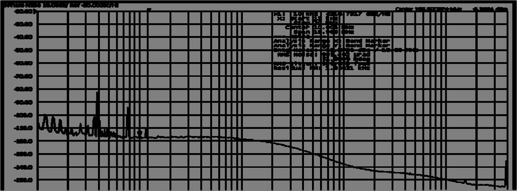

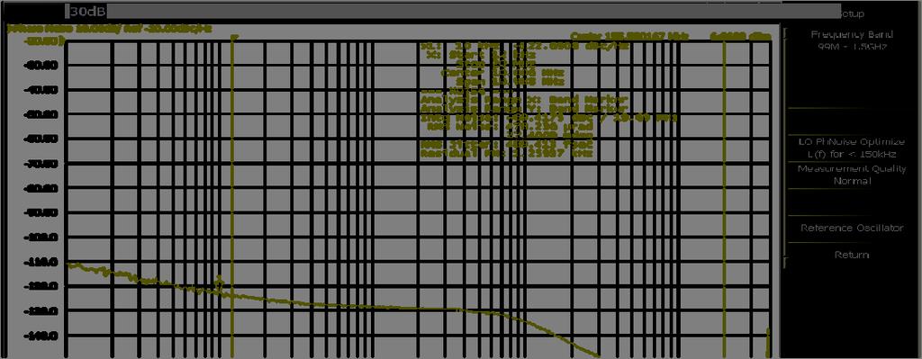

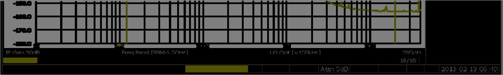

11 Phase Noise & Jitter Plots CARDINAL COMPONENTS, INC. Wayne, NJ of 15
12 Recommended Solder Profile for Cardinal Components, Inc. Package Infared Reflow. Do Not Use Ultrasonic-Wave Soldering or Wave Solder with Package Immersed in Solder Damage to Crystal will result. CARDINAL COMPONENTS, INC. Temperature (deg. ) Reliability Time (sec) Cardinal Components Inc., qualification includes aging at various extreme temperatures, shocks and vibration, temperature cycling, and IR reflow simulation. The Cappuccino family meets the following qualification tests: Environmental Compliance Parameter Conditions Mechanical Shock MIL-STD-883, Method 2002 Mechanical Vibration MIL-STD-883, Method 2007 Solderability MIL-STD-883, Method 2003 Gross and Fine Leak MIL-STD-883, Method 1014 Resistance to Solvents MIL-STD-883, Method 2016 Moisture Sensitivity Level IPC/ JEDEC J-STD-020, MSL1 Handling Precautions Although ESD protection circuitry has been designed into the Cappuccino proper precautions should be taken when handling and mounting. Cardinal employs a human body model (HBM) and a charged-device model (CDM) for ESD susceptibility testing and design protection evaluation. ESD Ratings Model Minimum Conditions Human Body Model 1000V MIL-STD-883, Method 3015 Charged Device Model 900V JEDEC, JESD22-C101 Machine Model 200V JEDEC, JESD22-A115-A Wayne, NJ of 15
13 Style 7: 5x7mm Ceramic Style 5: 5x3.2mm Ceramic 6 Pad LVDS/LVPECL 6 Pad LVDS/LVPECL Pin 1 OE Pin 1 OE Pin 2 Do Not Connect Pin 2 Do Not Connect Pin 3 GND Pin 3 GND Pin 4 Out Pin 4 Out Pin 5 nout Pin 5 nout Pin 6 V DD Pin 6 V DD Wayne, NJ of 15
14 Style 7P: 5x7mm Plastic Style 5P: 5x3.2mm Plastic 6 Pad LVDS/LVPECL Pin 1 OE Pin 2 Do Not Connect Pin 3 GND Pin 4 Out Pin 5 nout Pin 6 V DD Wayne, NJ of 15 6 Pad LVDS/LVPECL Pin 1 OE Pin 2 Do Not Connect Pin 3 GND Pin 4 Out Pin 5 nout Pin 6 V DD
15 Tape and Reel Specifications Model A B C Tape Specifications (mm) D E F STD QTY * CJAL/ CJAE ,000 Reel Specifications (mm) Model G H I J K L M CJAL/ CJAE Wayne, NJ of 15
CARDINAL COMPONENTS, INC.
 SERIES CJTDAE CJTDAL The Cardinal Cappuccino Crystal Oscillator LVDS/ LVPECL TCXO Features 3.3V supply voltage- configurable 10MHz to 250MHz LVDS and LVPECL outputs- configurable Better than 2Hz tuning
VT-820 VT-820. Temperature Compensated Crystal Oscillator Previous Vectron Model VTM3. Description
 VT-820 Temperature Compensated Crystal Oscillator Previous Vectron Model VTM3 VT-820 Description Vectron s VT-820 Temperature Compensated Crystal Oscillator (TCXO) is a quartz stabilized, clipped sine
VDD = V, TA = -40 C to +85 C, outputs terminated with 100 Ohms between Q and /Q.³
 Ultra-Low Jitter 200MHz LVDS XO ClockWorks FUSION General Description The is an ultra-low phase jitter XO with LVDS output optimized for high line rate applications. Features 200MHz LVDS Typical phase
CLEARCLOCK POWER OPTIMIZED 0.12ps 5x7mm XO
 FEATURES APPLICATIONS 0.125ps typ jitter (150fs MAX f > 200MHz, 25 C Highest in-class frequency range from 50 to 2100MHz Excellent spurious suppresion 70mA MAX I DD (LVDS, any V DD Lowest in-class power
Pin Configuration and Selector Guide appear at end of data sheet. Typical Operating Circuits
 Rev 2; 4/08 106.25MHz/212.5MHz/425MHz General Description The DS4106, DS4212, and DS4425 ceramic surfacemount crystal oscillators are part of Maxim s DS4-XO series of crystal oscillators. These devices
ESD Sensitive. Parameters Minimum Typical Maximum Units Notes ppm. Parameters Minimum Typical Maximum Units Notes
 Moisture Sensitivity Level (MSL) 1 FEATURES: LVCMOS, LVDS or LVPECL output option +2.5V or +3.3V operation -40 C to +85 C standard operating temperature range Ultra low RMS Jitter: 0.5ps typical, 1.0ps
User Selectable Up to Two Frequencies LVDS, LVPECL OR CMOS. 6 Pad Standard Package
 MVQI Series 5X7 Ceramic SMD VCXO User Selectable Up to Two Frequencies LVDS, LVPECL OR CMOS 6 Pad Standard Package OneClock Range CMOS Range LVDS & LVPECL Temperature Stability* Operating Temperature Range
PERFORMANCE PLASTIC PACKAGE ULTRA MINIATURE PURE SILICON TM CLOCK OSCILLATOR
 STANDARD SPECIFICATIONS: Moisture Sensitivity Level MSL 1 APPLICATIONS: FEATURES: Ultra Miniature Pure Silicon TM Clock Oscillator High Performance MEMS Technology by Discera Low Power Consumption for
STANDARD SPECIFICATIONS:
 Moisture Sensitivity Level MSL 1 FEATURES: APPLICATIONS: Ultra Miniature Pure SiliconTM Clock Oscillator Storage Area Networks (SATA, SAS, Fiber Channel) High Performance MEMS Technology by Discera Passive
Control Circuitry 2 M1. Micrel Inc Fortune Drive San Jose, CA USA tel +1 (408) fax + 1 (408)
 fax + 1 (408)") Crystal-less Configurable Clock Generator General Description The is a programmable, high performance dual LVDS output oscillator utilizing Micrel's proven silicon MEMS technology to provide excellent
Crystal-less Configurable Clock Generator General Description The is a programmable, high performance dual LVDS output oscillator utilizing Micrel's proven silicon MEMS technology to provide excellent
2:1 MULTIPLEXER CHIP FOR PCI-EXPRESS ICS Description. Features. Block Diagram DATASHEET
 DATASHEET 2:1 MULTIPLEXER CHIP FOR PCI-EXPRESS ICS557-08 Description The ICS557-08 is a 2:1 multiplexer chip that allows the user to select one of the two HCSL (Host Clock Signal Level) or LVDS input pairs
PERFORMANCE PLASTIC PACKAGE ULTRA MINIATURE PURE SILICON TM CLOCK OSCILLATOR ASEMP
 Moisture Sensitivity Level MSL 1 APPLICATIONS: FEATURES: Ultra Miniature Pure Silicon TM Clock Oscillator High Performance MEMS Technology by Discera Low Power Consumption for high speed communication
2:1 MULTIPLEXER CHIP FOR PCI-EXPRESS ICS Features
 DATASHEET 2:1 MULTIPLEXER CHIP FOR PCI-EXPRESS ICS557-08 Description The ICS557-08 is a 2:1 multiplexer chip that allows the user to select one of the two HCSL (Host Clock Signal Level) input pairs and
Ultra-Low Phase Jitter LVDS SMD Clock Oscillator
 Ultra-Low Phase Jitter LDS SMD Clock Oscillator ESD Sensitive Moisture Sensitivity Level MSL 3 FEATURES: 50MHz LDS Typical phase noise: 121fs (Integration range: 1.875MHz-20MHz) ±50ppm total frequency
DSC Q0093. General Description. Features. Applications. Block Diagram. Crystal-less Configurable Clock Generator
 Crystal-less Configurable Clock Generator General Description The is a four output crystal-less clock generator. It utilizes Microchip's proven PureSilicon MEMS technology to provide excellent jitter and
Features. o HCSL, LVPECL, or LVDS o Mixed Outputs: LVPECL/HCSL/LVDS. o Ext. Industrial: -40 to 105 C o o. o 30% lower than competing devices
 DSC55704 Crystalless Three Output PCIe Clock Generator General Description The DSC55704 is a Crystalless, three output PCI express clock generator meeting Gen1, Gen2, and Gen3 specifications. The clock
DSC2033. Low-Jitter Configurable Dual LVDS Oscillator. General Description. Features. Block Diagram. Applications
 General Description The series of high performance dual output LVDS oscillators utilize a proven silicon MEMS technology to provide excellent jitter and stability while incorporating additional device
TF90LVDS047-6CG. Quad LVDS Line Driver with Flow-Through Pinout. Description. Features. Applications. Function Diagram. Ordering Information
 Features Companion driver to Quad Extended Common Mode LVDS Receiver TF0LVDS048 DC to 400 Mbps / 200 MHz low noise, low skew, low power operation t 350 ps (max) channel-to-channel skew t 250 ps (max) pulse
Ultra-Low Phase Jitter LVPECL SMD Clock Oscillator
 Ultra-Low Phase Jitter LPECL SMD Clock Oscillator ESD Sensitive Moisture Sensitivity Level MSL 3 APPLICATIONS: 10/40/400 Gigabit Ethernet Fibre Channel 10G/12G SERDES FEATURES: 156.25MHz LPECL Typical
2 TO 4 DIFFERENTIAL CLOCK MUX ICS Features
 DATASHEET 2 TO 4 DIFFERENTIAL CLOCK MUX ICS557-06 Description The ICS557-06 is a two to four differential clock mux designed for use in PCI-Express applications. The device selects one of the two differential
CARDINAL COMPONENTS. FREQUENCY A MHz. Specifications: Min Typ Max Unit
 Re-Configurable 6 Output PECL TCXO Fixed & Re-Configurable Multi-Frequency Oscillator Intuitive software and I 2 C interface Easily update system Industry-standard packaging saves on board space Mult.
PI6C557-01BQ. PCIe 3.0 Clock Generator with 1 HCSL Outputs. Features. Description. Pin Configuration (16-Pin TQFN) Block Diagram
 Block Diagram") s Features ÎÎPCIe 3.0 compliant à à Phase jitter - 0.45ps RMS (High Freq. Typ.) ÎÎLVDS compatible output ÎÎSupply voltage of 3.3V ±10% ÎÎ25MHz crystal or clock input frequency ÎÎHCSL outputs, 0.8V Current
s Features ÎÎPCIe 3.0 compliant à à Phase jitter - 0.45ps RMS (High Freq. Typ.) ÎÎLVDS compatible output ÎÎSupply voltage of 3.3V ±10% ÎÎ25MHz crystal or clock input frequency ÎÎHCSL outputs, 0.8V Current
CARDINAL COMPONENTS. Specifications: Min Typ Max Unit
 Re-Configurable 6 Output CMOS TCXO Fixed & Re-Configurable Multi-Frequency Oscillator Intuitive software and I 2 C interface Easily update system Software flexible, quick upgrades and changes Industry-standard
Control Circuitry 2 M1. Micrel Inc Fortune Drive San Jose, CA USA tel +1 (408) fax + 1 (408)
 fax + 1 (408)") DSC2044FE1H0002 Crystalless Configurable Clock Generator General Description The DSC2044FE1H0002 is a programmable, high performance dual HCSL output oscillator utilizing Micrel's proven silicon MEMS technology
DSC2044FE1H0002 Crystalless Configurable Clock Generator General Description The DSC2044FE1H0002 is a programmable, high performance dual HCSL output oscillator utilizing Micrel's proven silicon MEMS technology
Features. Applications
 HCSL-Compatible Clock Generator for PCI Express General Description The is the smallest, high performance, lowest power, 2 differential output clock IC available for HCSL timing applications. offers -130dBc
Ultra-Low Phase Jitter LVPECL SMD Clock Oscillator
 Ultra-Low Phase Jitter LPECL SMD Clock Oscillator ASMX-156.250MHz-3BNR ESD Sensitive Moisture Sensitivity Level MSL 3 APPLICATIONS: 10/40/400 Gigabit Ethernet Fibre Channel 10G/12G SERDES FEATURES: 156.25MHz
Micrel Inc Fortune Drive San Jose, CA USA tel +1 (408) fax + 1 (408)
 fax + 1 (408)") DSC2311KL2R008 Crystalless Configurable Clock Generator General Description DSC2311KL2R008 is a crystalless clock generator that is factory configurable to simultaneously output two separate frequencies
DSC2311KL2R008 Crystalless Configurable Clock Generator General Description DSC2311KL2R008 is a crystalless clock generator that is factory configurable to simultaneously output two separate frequencies
TF10CP02 / TF10CP Gbps 2x2 LVDS Crosspoint Switches. Features. Description. Applications. Function Diagram. Ordering Information.
 Features DC to 1.5 Gbps low jitter, low skew, low power operation Pin configurable, fully differential, non-blocking architecture eases system design and PCB layout On-chip 100W input termination minimizes
3.3V CMOS/PECL/LVDS OUTPUT SMD VCXO
 FEATURES: CMOS, PECL or LVDS Output Low Integrated rms jitter (1 max. over 12kHz to 20MHz BW) Low Profile, Seam-Sealed Package (5.08 x 7.0 x1.8mm) Wide Frequency Pull Range (±100 ppm min.) Pb RoHS/RoHS
CARDINAL COMPONENTS. Specifications: Min Typ Max Unit
 Re-Configurable 4 Output CMOS Oscillator Fixed & Re-Configurable Multi-Frequency Oscillator Intuitive software and I 2 C interface Easily update system Software flexible, quick upgrades and changes Industry-standard
3SM201KMF0KB MEMS Microphone
 Product Description The is a monolithic MEMS top performing miniature digital microphone based on CMOS foundry process. By integrating an acoustic transducer and an analog amplifier circuit followed by
PI6LC48L0201A 2-Output LVDS Networking Clock Generator
 Features ÎÎTwo differential LVDS output pairs ÎÎSelectable crystal oscillator interface or LVCMOS/LVTTL single-ended clock input ÎÎSupports the following output frequencies: 62.5MHz, 125MHz, 156.25MHz
FIN1101 LVDS Single Port High Speed Repeater
 FIN1101 LVDS Single Port High Speed Repeater General Description This single port repeater is designed for high speed interconnects utilizing Low Voltage Differential Signaling (LVDS) technology. It accepts
3SM201KMT1KB MEMS Microphone
 MEMS Microphone Product Description The is a monolithic MEMS top performing miniature digital microphone based on CMOS foundry process. By integrating an acoustic transducer and an analog amplifier circuit
FIN1102 LVDS 2 Port High Speed Repeater
 LVDS 2 Port High Speed Repeater General Description This 2 port repeater is designed for high speed interconnects utilizing Low Voltage Differential Signaling (LVDS) technology. The FIN1102 accepts and
T1/E1 CLOCK MULTIPLIER. Features
 DATASHEET ICS548-05 Description The ICS548-05 is a low-cost, low-jitter, high-performace clock synthesizer designed to produce x16 and x24 clocks from T1 and E1 frequencies. Using IDT s patented analog/digital
SM General Description. Features. Block Diagram. ClockWorks TM 125MHz LVDS / 125 MHz HCSL Ultra-Low Jitter Frequency Synthesizer
 ClockWorks TM 125MHz LVDS / 125 MHz HCSL Ultra-Low Jitter Frequency Synthesizer General Description The is a member of the ClockWorks family of devices from Micrel and provides an extremely low-noise timing
SM Features. General Description. Typical Application MHz/312.5MHz and MHz/156.25MHz LVDS Clock Synthesizer.
 156.25MHz/312.5MHz and 78.125MHz/156.25MHz LVDS Clock Synthesizer ClockWorks Flex General Description The is a member of the ClockWorks family of devices from Micrel and provides an extremely low-noise
PI6C Low Power Networking Clock Generator. Description. Features. Block Diagram. 100MHz PCI-Express 0 100MHz PCI-Express 1 100MHz PCI-Express 2
 Features ÎÎ25 MHz crystal or clock input ÎÎThree differential 100 MHz PCI-Express clock outputs push-pull termination ÎÎSpread spectrum capability on all 100 MHz PCI-e clock outputs with -0.5% down spread
PCIe 3.0 Clock Generator with 4 HCSL Outputs. Description OE VDDXD S0 S1 S2 X1 X2 PD OE GNDXD IREF CLK0 CLK0 CLK1 CLK1 CLK2 CLK2 CLK3 CLK3
 PCIe 3.0 Clock Generator with 4 HCSL Outputs Features PCIe 3.0 complaint PCIe 3.0 Phase jitter: 0.48ps RMS (High Freq. Typ.) LVDS compatible outputs Supply voltage of 3.3V ±5% 25MHz crystal or clock input
Features. Applications
 Ultra-Precision 1:8 CML Fanout Buffer with Internal I/O Termination General Description The is a 2.5V/3.3V precision, high-speed, fully differential CML 1:8 fanout buffer. The is optimized to provide eight
VM1000 Low Noise Bottom Port Analog Single-Ended Piezoelectric MEMS Microphone
 GENERAL DESCRIPTION Vesper presents the world s first piezoelectric MEMS microphone. The provides superior performance and quality in all environments. The is a low noise, high dynamic range, single-ended
CKSET V CC _VCO FIL SDO+ MAX3952 SCLKO+ SCLKO- PRBSEN LOCK GND TTL
 19-2405; Rev 0; 4/02 10Gbps 16:1 Serializer General Description The 16:1 serializer is optimized for 10.3Gbps and 9.95Gbps Ethernet applications. A serial clock output is provided for retiming the data
CAP+ CAP. Loop Filter
 STS-12/STS-3 Multirate Clock and Data Recovery Unit FEATURES Performs clock and data recovery for 622.08 Mbps (STS-12/OC-12/STM-4) or 155.52 Mbps (STS-3/OC-3/STM-1) NRZ data 19.44 MHz reference frequency
SGM Channel, 6th-Order Video Filter Driver for SD/HD
 PRODUCT DESCRIPTION The SGM9346 video filter is intended to replace passive LC filters and drivers with an integrated device. Six 6th-order Butterworth filters provide improved image quality compared to
ICS548A-03 LOW SKEW CLOCK INVERTER AND DIVIDER. Description. Features. Block Diagram DATASHEET
 DATASHEET ICS548A-03 Description The ICS548A-03 is a low cost, low skew, high-performance general purpose clock designed to produce a set of one output clock, one inverted output clock, and one clock divided-by-two.
Monolithic Amplifier CMA-252LN+ Ultra Low Noise, High IP to 2.5 GHz. The Big Deal
 Ultra Low, High IP3 Monolithic Amplifier 50Ω The Big Deal 1.5 to 2.5 GHz Ceramic, Hermetically Sealed, Nitrogen filled Low profile case,.045 high Ultra Low High Gain, High IP3 Class 1B HBM ESD (500V) CASE
SM Features. General Description. Applications. Block Diagram
 ClockWorks Fibre Channel (106.25MHz, 212.5MHz) Ultra-Low Jitter, LVDS Frequency Synthesizer General Description The is a member of the ClockWorks family of devices from Micrel and provides an extremely
XRD87L85 Low-Voltage CMOS 8-Bit High-Speed Analog-to-Digital Converter
 Low-Voltage CMOS 8-Bit High-Speed Analog-to-Digital Converter April 2002-1 FEATURES 8-Bit Resolution Up to 10 MHz Sampling Rate Internal S/H Function Single Supply: 3.3V VIN DC Range: 0V to V DD VREF DC
3SM102EZT13C MEMS Microphone
 Product Description The brings excellent performance on the applications of ANC headphone, TWS headset, Beam-forming device and Voice Recognition device by the unique features of tiny package size, flat
VCXO. Contact Sales. North America T: +1 (800) Asia T: All Other Regions T: +1 (508)
 Asia T: All Other Regions T: +1 (508)") Contact Sales North America T: +1 (800) 982-5737 Asia T: +65-6481-1466 All Other Regions T: +1 (508) 435-6831 frequencysales@ctscorp.com www.ctscorp.com 2016.10 - KGC CTS broad portfolio of Voltage Controlled
Contact Sales North America T: +1 (800) 982-5737 Asia T: +65-6481-1466 All Other Regions T: +1 (508) 435-6831 frequencysales@ctscorp.com www.ctscorp.com 2016.10 - KGC CTS broad portfolio of Voltage Controlled
XRD8775 CMOS 8-Bit High Speed Analog-to-Digital Converter
 CMOS 8-Bit High Speed Analog-to-Digital Converter April 2002-4 FEATURES 8-Bit Resolution Up to 20MHz Sampling Rate Internal S/H Function Single Supply: 5V V IN DC Range: 0V to V DD V REF DC Range: 1V to
Wireless Access Point Server/Storage DIFF1 DIFF2
 PCI-EXPRESS GEN 1, GEN 2, AND GEN 3 1:2 FAN-OUT CLOCK BUFFER Features PCI-Express Gen 1, Gen 2, and Gen 3 compliant devices Two low-power PCIe clock outputs Supports Serial-ATA (SATA) at 100 MHz No termination
Low-Noise Bottom Port Piezoelectric MEMS Microphone
 Low-Noise Bottom Port Piezoelectric MEMS Microphone Data Sheet PMM-3738-VM1000-R PUI Audio, featuring Vesper s exclusive technology, presents the world s first and only piezoelectric MEMS microphone. The
SCA620-EF1V1B SINGLE AXIS ACCELEROMETER WITH ANALOG INTERFACE
 Datasheet SCA620-EF1V1B SINGLE AXIS ACCELEROMETER WITH ANALOG INTERFACE The SCA620 accelerometer consists of a silicon bulk micro machined sensing element chip and a signal conditioning ASIC. The chips
LVDS Crystal Oscillator (XO)
") LVDS Crystal Oscillator (XO) Features Low jitter crystal oscillator (XO) Less than 1 ps typical root mean square (RMS) phase jitter Low-voltage differential signaling (LVDS) output Output frequency from
LVDS Crystal Oscillator (XO) Features Low jitter crystal oscillator (XO) Less than 1 ps typical root mean square (RMS) phase jitter Low-voltage differential signaling (LVDS) output Output frequency from
SP1050 Series for Power-over-Ethernet PSE Protection
 SP1050 Series for Power-over-Ethernet PSE Protection RoHS Pb GREEN Description The SP1050-04BTG provides over-voltage protection for Power-over-Ethernet PSE equipment in a space saving SOIC-8 package.
Features. Applications
 6GHz, 1:4 CML Fanout Buffer/Translator with Internal I/O Termination General Description The is a 2.5V/3.3V precision, high-speed, fully differential 1:4 CML fanout buffer. Optimized to provide four identical
3SM122HZB1VA MEMS Microphone
 Product Description The microphones are integrated with specialized pre-amplification ASIC to provide high sensitivity, high SNR output from a capacitive audio sensor. It s packaged for surface mounting
Omnidirectional Microphone with Bottom Port and Analog Output ADMP401
 FEATURES 4.72 mm 3.76 mm 1.0 mm surface-mount package High SNR of 62 dba Sensitivity of 42 dbv Flat frequency response from 100 Hz to 15 khz Low current consumption of
Typical Applications Base Stations C MHz 700 MHz. Reference Frequency. Parameter Min Typ Max Units Condition
 FX-401 Frequency Controlled Crystal Oscillator Features Reflow Process Compatible Surface Mount Package Low Phase Noise Build in PLL-Circuit Typical Applications Base Stations Previous Vectron Model Number
PI6CEQ PCIe Gen2 / Gen3 Buffer. Features. Description. Applications. Block Diagram. Pin Configuration (20-Pin TSSOP & 20-Pin QSOP)
") PCIe Gen2 / Gen3 Buffer Features ÎÎPCIe Gen2/ Gen3* compliant clock buffer/zdb * Gen3 performance only available in Commercial temp ÎÎInternal equalization for better signal integrity ÎÎ2 HCSL outputs
PCIe Gen2 / Gen3 Buffer Features ÎÎPCIe Gen2/ Gen3* compliant clock buffer/zdb * Gen3 performance only available in Commercial temp ÎÎInternal equalization for better signal integrity ÎÎ2 HCSL outputs
PI6C GHz 1:4 LVPECL Fanout Buffer with Internal Termination GND Q0+ Q0- REF_IN+ V TH V REF-AC REF_IN- Q1+ Q1- Q2+ Q2- Q3+ Q3- VDD.
 Features ÎÎInput Clock Frequency up to 6 GHz Typical ÎÎ4 pairs of differential LVPECL outputs ÎÎLow additive jitter, < 0.05ps (max) ÎÎInput CLK accepts: LVPECL, LVDS, CML, SSTL input level ÎÎOutput to
Industry Product Group
 Cosemitech (Shanghai) Co., Ltd. FEATURES and FUNCTIONAL DIAGRAM PACKAGE Enhanced sensitivity: will operate from only 45 Gauss typical, at 25 C allowing the use of smaller, potentially lower-cost magnets
FIN3385 FIN3383 Low Voltage 28-Bit Flat Panel Display Link Serializers
 October 2003 Revised January 2004 FIN3385 FIN3383 Low Voltage 28-Bit Flat Panel Display Link Serializers General Description The FIN3385 and FIN3383 transform 28 bit wide parallel LVTTL (Low Voltage TTL)
SP5001 Series 4 Channel TVS Common Mode Filter
 Low Capacitance ESD Protection - SP51 Series SP51 Series 4 Channel TVS Common Mode Filter RoHS Pb GREEN Description The SP51 Series is a highly integrated Common Mode Filter (CMF providing both ESD protection
ZL40218 Precision 1:8 LVDS Fanout Buffer
 Precision 1:8 LVDS Fanout Buffer Data Sheet Features Inputs/Outputs Accepts differential or single-ended input LVPECL, LVDS, CML, HCSL, LVCMOS Eight precision LVDS outputs Operating frequency up to 750
1000 Base-T, ±15kV ESD Protection LAN Switches
 19-0624; Rev 0; 8/06 1000 Base-T, ±15kV ESD Protection LAN Switches General Description The meet the needs of high-speed differential switching. The devices handle the needs of Gigabit Ethernet (10/100/1000)
HSP051-4N10. 4-line ESD protection for high speed lines. Applications. Description. Features. Benefits. Complies with following standards
 4-line ESD protection for high speed lines Datasheet production data Benefits High ESD protection level High integration Suitable for high density boards Figure 1. Functional schematic (top view) I/O 1
Features. Applications
 3.3V Ultra-Precision 1:4 LVDS Fanout Buffer/Translator with Internal Termination General Description The is a 3.3V, high-speed 2GHz differential low voltage differential swing (LVDS) 1:4 fanout buffer
OBSOLETE PI6C Low Power Networking Clock Generator. Description. Features. Block Diagram
 Features ÎÎ3.3V supply voltage ÎÎ25MHz XTAL or reference clock input ÎÎOutput 4x100MHz HCSL PCIe clock outputs with integrated series termination resistors, spread spectrum capability on all 100MHz PCIe
HSP051-4M10. 4-line ESD protection for high speed lines. Applications. Description. Features. Benefits. Complies with following standards
 4-line ESD protection for high speed lines Datasheet production data Benefits High ESD protection level High integration Suitable for high density boards Figure 1. Functional schematic (top view) I/O 1
ZL40223 Precision 2:8 LVDS Fanout Buffer with Glitchfree Input Reference Switching and On-Chip Input Termination Data Sheet
 Features Inputs/Outputs Accepts two differential or single-ended inputs LVPECL, LVDS, CML, HCSL, LVCMOS Glitch-free switching of references On-chip input termination and biasing for AC coupled inputs Eight
1, 2, 4 and 8-Channel Very Low Capacitance ESD Protectors
 1, 2, 4 and 8-Channel Very Low Capacitance ESD Protectors CM1210 Features 1,2,4 and 8 channels of ESD protection Very low loading capacitance (1.0pF typical) ±6 kv ESD protection per channel (IEC 61000-4-2
MX877RTR. 8-Channel, 60V Driver with Push-Pull Output, 3 Wire Interface INTEGRATED CIRCUITS DIVISION. Features. Description.
 8-Channel, 6V Driver with Push-Pull Output, 3 Wire Interface Features Eight (8) Outputs Rated at 6V, ±8mA Push-Pull Driver Configuration 6V to 6V Driver Supply Range 2.7V to 5.5V Logic Supply Range 3-Wire
Features. Applications
 2.5/3.3V 1-to-1 Differential to LVCMOS/LVTTL Translator Precision Edge General Description Micrel s is a 1-to-1, differential-to-lvcmos / LVTTL translator. The differential input is highly flexible and
Low Skew, 1-to-8, Differential-to-LVDS Clock
 Low Skew, 1-to-8, Differential-to-LVDS Clock 85408 DATA SHEET General Description The 85408 is a low skew, high performance 1-to-8 Differential-to-LVDS Clock Distribution Chip. The 85408 CLK, nclk pair
Digital "Mini" SiSonic TM Microphone Specification - Halogen Free. Knowles Acoustics 1151 Maplewood Drive Itasca, IL 60143
 Digital "Mini" SiSonic TM Microphone Specification - Halogen Free Knowles Acoustics 1151 Maplewood Drive Itasca, IL 60143 Sheet 1 of 11 1. DESCRIPTION AND APPLICATION 1.1 DESCRIPTION Digital "Mini" Surface
Not recommended for new designs
 Eight Output Differential Buffer for PCI-Express Recommended Application: DB800 Intel Yellow Cover part with PCI-Express support. Output Features: 8-0.7V current-mode differential output pairs Supports
1000 Base-T, ±15kV ESD Protection LAN Switch
 19-0841; Rev 0; 6/07 1000 Base-T, ±15kV ESD Protection LAN Switch General Description The meets the needs of high-speed differential switching, including that of Gigabit Ethernet (10/100/1000) Base-T switching
3SM102E4T12A MEMS Microphone
 MEMS Microphone Product Description The is a monolithic MEMS top performing miniature analog microphone based on CMOS foundry process. By integrating an acoustic transducer and an analog amplifier circuit
SY89610L. General Description. Features. Applications MHz to 694MHz Jitter Attenuator and Low Phase Noise Frequency Synthesizer
 77.75MHz to 694MHz Jitter Attenuator and Low Phase Noise Frequency Synthesizer General Description The is a 3.3V, fully differential jitter attenuator and frequency synthesizer that accepts a noise clock
3SM102E4T13B MEMS Microphone
 MEMS Microphone Product Description The is a monolithic MEMS top performing miniature analog microphone based on CMOS foundry process. By integrating an acoustic transducer and an analog amplifier circuit
MLSEP*** Series. Multilayer Polymer ESD Suppressor. Features. Application. Electrical Characteristics
 Features ESD protection for high speed data lines to IEC61000-4-2 ESD contact discharge typical 8KV, max 15KV IEC61000-4-2 ESD air discharge typical 15KV, max 25KV Protect four data lines Flow through
HSP051-4M10. 4-line ESD protection for high speed lines. Datasheet. Features. Applications. Description
 Datasheet 4-line ESD protection for high speed lines Features I/O 1 I/O 2 GND 3 I/O 3 I/O 4 1 2 4 µqfn-10l package Functional schematic (top view) 10 9 8 7 5 6 Internal ly not connected GND Internal ly
HSP061-4M10. 4-line ESD protection for high speed lines. Datasheet. Features. Applications. Description
 Datasheet 4-line ESD protection for high speed lines Features I/O I/O 2 GND 3 I/O 3 I/O 4 2 4 µqfn-0l package Functional schematic (top view) 0 9 8 7 5 6 Product status HSP06-4M0 Internal ly not connected
Monolithic Amplifier CMA-545G1+ Low Noise, High IP to 2.2 GHz. The Big Deal
 Low Noise, High IP3 Monolithic Amplifier 50Ω The Big Deal 0.4 to 2.2 GHz Ceramic, Hermetically Sealed, Nitrogen filled Low profile case,.045 high High Gain, 31.5 db Low Noise Figure, 1.0 db High IP3, 35-37
Knowles Acoustics 1151 Maplewood Drive Itasca, IL 60143
 Zero Height SiSonic Microphone Specification Knowles Acoustics 1151 Maplewood Drive Itasca, IL 60143 1of 10 1. DESCRIPTION AND APPLICATION 1.1 Description Zero Height Surface Mount Silicon Microphone 1.2
PART. *EP = Exposed pad. LVDS IN+ IN- PCB OR TWISTED PAIR. Maxim Integrated Products 1
 19-0849; Rev 1; 12/07 10-Bit LVDS Serializer General Description The serializer transforms 10-bit-wide parallel LVCMOS/LVTTL data into a serial high-speed, low-voltage differential signaling (LVDS) data
Technical Data Sheet Photolink- Fiber Optic Receiver
 Technical Data Sheet Photolink- Fiber Optic Receiver Features 1. High PD sensitivity optimized for red light 2. Data : NRZ signal 3. Low power consumption for extended battery life 4. Built-in threshold
4bit LVDS Driver BU90LV047A. LVDS Interface ICs
 LVDS Interface ICs 4bit LVDS Driver BU90LV047A Description LVDS Interface IC of ROHM "Serializer" "Deserializer" operate from 8MHz to 150MHz wide clock range, and number of bits range is from 35 to 70.
Q-TECH CORPORATION. QT2024L CMOS, LOW CURRENT HIGH-TEMPERATURE REAL TIME CLOCK I 2 C SERIAL BUS INTERFACE 3.3Vdc. Description. Electrical Parameters
 Description The QT2024 is an I 2 C-bus serial interface conforming, highprecision real-time clock (RTC) IC with a built-in 32.768kHz crystal oscillator circuit. In addition to clock and calendar functions,
BLOCK DIAGRAM PIN ASSIGNMENT ICS LOW SKEW, DUAL, 1-TO-5 DIFFERENTIAL- TO-LVDS FANOUT BUFFER PRELIMINARY ICS854210
 LOW SKEW, DUAL, 1-TO-5 DIFFERENTIAL- TO-LVDS FANOUT BUFFER ICS854210 GENERAL DESCRIPTION The ICS854210 is a low skew, high performance ICS dual 1-to-5 Differential-to-LVDS Fanout Buffer HiPerClockS and
SPECIFICATION Of CMOS MEMS Analog Microphone. Model No.: JL-M2417
 SPECIFICATION Of CMOS MEMS Analog Microphone ( RoHS Compliance ) : : ISSUED BY J.C 09-27-2012 CHECKED BY APPROVED BY Version 00 Pages 1 / 11 Revision History Version Description Date Author Approved 00
SP2574NUTG 2.5V 40A Diode Array
 TVS Diode Arrays (SPA Diodes 2.5V 40A Diode Array RoHS Pb GREEN Description The is a low-capacitance, TVS Diode Array designed to provide protection against ESD (electrostatic discharge, CDE (cable discharge
Triangular spread spectrum profile for maximum EMI reduction (Si50122-A2) 2.5 V, 3.3 V Power supply. (2.0 x 2.5 mm) down spread outputs
 2.5 V, 3.3 V Power supply. (2.0 x 2.5 mm) down spread outputs") CRYSTAL-LESS PCI-EXPRESS GEN1 DUAL OUTPUT CLOCK GENERATOR Features Crystal-less clock generator with integrated CMEMS PCI-Express Gen 1 compliant Triangular spread spectrum profile for maximum EMI reduction
CRYSTAL-LESS PCI-EXPRESS GEN1 DUAL OUTPUT CLOCK GENERATOR Features Crystal-less clock generator with integrated CMEMS PCI-Express Gen 1 compliant Triangular spread spectrum profile for maximum EMI reduction
Programmable CMOS LVDS Transmitter/Receiver
 SPECIFICATION 1. FEATURES Technology TSMC 0.13um CMOS 3.3 V analog power supply 1.2 V digital power supply 1.2V CMOS input and output logic signals 8-step (3-bit) adjustable transmitter output current
Accelerate the speed of circuit design...oscillators in seconds, not days!
 Accelerate the speed of circuit design...oscillators in seconds, not days! The MEMSpeed Pro oscillators operate down to 4mA with 1uA standby current! Introducing the MEMSpeed Pro, Low Power Oscillator
PI2PCIE2214. PCI Express 2.0, 1-lane, 4:1 Mux/DeMux Switch. Features. Description. Application. Pin Description. Block Diagram.
 Features 2 Differential Channel, 4:1 Mux/DeMux PCI Express 2.0 performance, 5.0 Gbps Low Bit-to-Bit Skew, 7ps Max. Low Crosstalk: -23dB@3GHz Low Off Isolation: -23dB@3GHz Operating Range: 1.8V ±10% ESD
SP1124T Discrete Unidirectional TVS Diode
 SP1124T Discrete Unidirectional TVS Diode RoHS Pb GREEN Description This TVS diode is fabricated in a proprietary silicon avalanche technology and is used for high level protection of electronic equipment