Couture: Tailoring STT-MRAM for Persistent Main Memory
|
|
|
- Charlene Cole
- 6 years ago
- Views:
Transcription


 has been instrumental in propelling the progress of computer systems, serving as the")


![While prior studies addressed these challenges using techniques such as data partitioning [2] and retentionaware refresh [3], it is](/docs-images/74/70732311/images/1-22.jpg "expected that replacing with a non-volatile memory (NVM) can alleviate the power and reliability issues in the long term [4].")

 is roughly six times larger than a cell ( 6F 2 ), which renders it difficult for STT- MRAM to")
 4KB Page (b) Figure 1: The reduction in cell area by the proposed optimizations in our design (a), and an analysis of")


1 : Tailoring for Persistent Main Memory Abstract Modern computer systems rely extensively on dynamic random-access memory () to bridge the performance gap between on-chip cache and secondary storage. However, continuous process scaling has exposed to high off-state leakage and excessive power consumption from frequent refresh operations. Spintransfer torque magnetoresistive RAM () is a plausible replacement for, given its high endurance and near-zero leakage. However, conventional cannot directly substitute due to its large cell space area and the high latency and energy costs for writes. In this work, we present a main memory design using tailored that can offer a storage density comparable to and high performance with low-power consumption. In addition, we propose an intelligent data scrubbing method (iscrub) to ensure data integrity with minimum overhead. Our evaluation results show that, equipped with the iscrub policy, our proposed can achieve up to 23% performance improvement, while consuming 18% less energy, on average, compared to a contemporary. 1 Introduction Dynamic random-access memory () has been instrumental in propelling the progress of computer systems, serving as the exclusive main memory technology. However, many recent data-intensive applications are demanding terabytes of working memory [1], forcing to scale-down to smaller process technologies that can adversely affect its performance and reliability. Specifically, scaling down cells increases off-state leakage, and reduces data-retention time. This results in frequent refresh operations that burden with extra latency and power overhead. The increased leakage also renders less reliable, as leakage from the off cells into the bitlines can generate errors. While prior studies addressed these challenges using techniques such as data partitioning [2] and retentionaware refresh [3], it is expected that replacing with a non-volatile memory (NVM) can alleviate the power and reliability issues in the long term [4]. Spintransfer torque magnetoresistive random-access memory () has received considerable attention as one such replacement candidate, owing to its excellent scalability, endurance, and near-zero leakage [4]. However, the primary obstruction in replacing with STT- MRAM is their difference in cell area. A typical STT- MRAM cell ( 40F 2 ) is roughly six times larger than a cell ( 6F 2 ), which renders it difficult for STT- MRAM to attain the density required for main mem- Conventional ECC 0.001% (a) 4KB Page (b) Figure 1: The reduction in cell area by the proposed optimizations in our design (a), and an analysis of retention errors in tailored (b). ory. The other critical challenge with is that, its write process involves physically switching the magnetic configuration of the magnetic tunnel junction (MTJ) with a large write current rendering the energy cost unsuitable for write-intensive applications. In this work, we present, a persistent main memory that tailors to offer a comparable storage density, along with low-power operation, and excellent read/write performance. Specifically, we propose to tune the MTJ s thermal stability factor to lower the write current, which allows to use smaller access transistors and significantly reduce its cell area. Figure 1a demonstrates this cell area reduction achieved by our design. By lowering the write current, we also reduce s write energy. Furthermore, we present an optimized DDR3 [5] based dual in-line memory module (DIMM) design for our tailored. Unfortunately, optimizing the thermal stability factor partially truncates the conventional data retention time of the ( 10 years). In addition, at the end of the retention period, the cells experience an increased probability of unintentional switching of the MTJs and can generate errors, which in turn can render difficult to be a reliable persistent working memory. Figure 1b demonstrates that, a small rise in the 1
2 Figure 2: Internal structure of the cell. cell-level switching probability can escalate the error rate in a 4KB memory page, overwhelming the typical singleerror correction and double-error detection (SECDED) ECC [6]. To address this, we propose iscrub, a novel data-scrubbing scheme using reinforcement learning to ensure data persistency with minimum overhead. The main contributions of this work are as follows: Tailored. We tune the MTJ design parameters to render the cell area comparable to that of a modern. Specifically, we adjust the thermal stability factor to lower the critical current for switching the MTJ s orientation, which in turn enables us to reduce s cell area and its write energy. Revamped memory module. We propose a modified DIMM that incorporates unique requirements of STT- MRAM, while maintaining main memory s fundamental organization and DDR interface. Reinforcement learning for intelligent scrubbing. We employ a customized reinforcement learning algorithm to minimize the latency and power overhead caused by scrub operation in tailored without incurring additional retention errors. In this work, we compare our memory and a DDR3 at system-level, and the evaluation results show that our with iscrub can deliver up to a 23% performance gain, while consuming 18% less energy, on average. 2 Preliminary 2.1 Fundamentals Cell structure. Figure 2 shows the cell structure of STT- MRAM, which consists of an access transistor and a magnetic tunnel junction (MTJ). The access transistor is used to activate and control the cell, while MTJ works as the storage element. The MTJ demonstrates two different resistance levels by switching the polarity of its ferromagnetic plates to either parallel or anti-parallel configuration. These two resistance levels are used to represent the stored data bit (0 or 1) [7]. Characteristics of basic operations. The read operation of is fast and power-efficient, because sense amplifier only needs to inject small current to measure the resistance of target cells. However, a large current is required to switch the the target MTJ s free layer orientation during a write operation, which results in high write energy and large cell size. Specifically, to avoid write failures, transistors with a large W/L ratio are used to drive the write current, which in turn increases the cell size [8]. 2.2 Exploring Critical Design Parameters Thermal stability factor ( ). In order to ensure data storage reliability, the MTJ in a cell must maintain the parallel and the anti-parallel configurations in a discrete and stable manner. Thermal stability factor refers to the stability of an MTJ s magnetic orientation, and is modeled as [9]: E b H KM S V 2k B T where E b is energy barrier, T is temperature, H K is anisotropic field, M S is saturation magnetization, k B is Boltzmann constant, and V is MTJ s volume. One can note that, while the other parameters are fixed, we can set the thermal stability factor to fit our optimization goal by modifying the MTJ s volume. Critical current (I C ). Critical current refers to minimum current that switches the polarity of MTJ s free layer [9]. The model for critical current can be expressed as: (1) I C = γ[ + δv T ] (2) where γ and δ are fitting constants that represent the operational environment, V is MTJ s volume, and T is temperature. The analytic model reveals that, critical current (I C ) can be reduced by reducing thermal stability factor ( ). Retention time. Retention time is the expected time before a random bit-flip occurs. It depends on the thermal stability factor, and can be expressed as follows [9]: T Retention = 1 f 0 exp( ) (3) where f 0 is the operating frequency. One can notice that, while a low thermal stability factor reduces the MTJ s critical current requirement, unfortunately, it also shortens the retention time. 3 Persistent Main Memory 3.1 Tailoring Access transistor optimization. A cell is comprised of one access transistor and one MTJ. Since MTJ has comparatively small size, access transistor size becomes the main factor of cell area. As access transistor is used to control current to go through MTJ, the transistor size is mainly decided by the maximum current. Thus, in order to minimize the cell area, the critical current should be reduced. Equations 1 3 indicate the relationship of thermal stability factor and critical current. Derived from Equations 1 3, we evaluate shows the optimized cell areas under the reduced thermal stability factors, and the results are shown in Figure 3a. One can observe from this figure that as the thermal stability factor decreases, the cell area keeps decreasing. However, it also shows that, the lowering of thermal stability factor ( ) also shortens the retention 2
 Write Power (uw) 100 Write Power 90 Write Latency 80 70 60")
 vs. cell area and retention time (a), write current vs. write power and write latency (b), and thermal stability factor ( ) vs.")


 per rank.")


.")

 running at 800 MHz to the internal address (IAB) and data bus (IDB), respectively.")
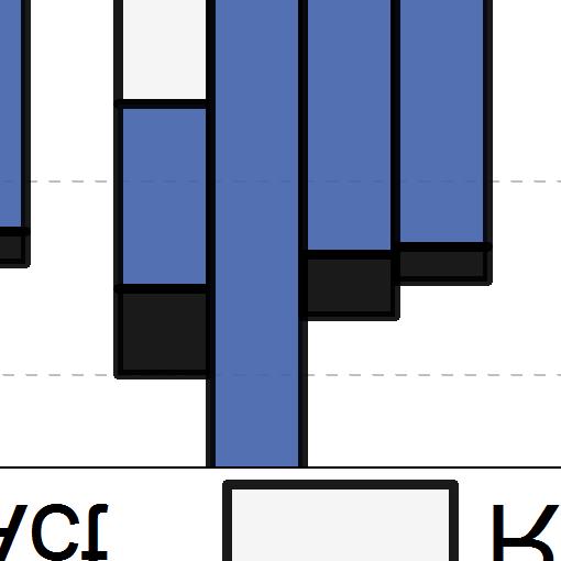
3 Cell Area (F 2 ) 50 Cell Area 40 Retention Thermal Stability Factor Retention (hours) Write Power (uw) 100 Write Power 90 Write Latency Write Current (ua) (a) (b) (c) Figure 3: Cell-level optimization of the : thermal stability factor ( ) vs. cell area and retention time (a), write current vs. write power and write latency (b), and thermal stability factor ( ) vs. write energy (c) Write Latency (ns) Write Energy (pj) Write Energy time of our tailored optimization. By considering the trade-off between the cell size and retention time, we shorten the thermal stability factor from to by reducing MTJ volume and the cell area is reduced from 36 F 2 to 10 F 2. While the cell area of our tailored is not equal to that of, it attains a practically comparable size. Energy and latency optimization. We also derived the relationship of write current and write power as well as write current and write latency, which is shown in Figure 3b. It is crucial to note that lowering the write current in order to reduce the write power only marginally increases the write latency. In fact, reducing the write current can significantly improve the overall write energy. As shown in Figure 3c, when we lower the thermal stability factor from its default value of 40.3 to 28.9, the s write energy actually decreases from 0.66 pj to 0.44 pj. Figure 4: Proposed main memory. 3.2 Memory Module Design Memory module organization. To ensure a smooth transition from, we designed our proposed such that it can fit in existing main memory infrastructure, with only minimal changes to the host system. Therefore, we used a modified DIMM with the DDR3 PC interface to implement our proposed design. Our configuration follows the consumer architecture and has two ranks per module and eight x8 memory chips (+1 ECC chip) per rank. Figure 4 illustrates the organization of our design. Similar to, each rank is logically divided into eight banks, and each bank is further divided into subarrays. Whereas global address decoders and row buffers are assigned to each bank, subarrays are internally accessed using local address decoders and row buffers. Individual memory cells, consisting of an access transistor and an MTJ, are connected via a bitline (BL), a sourceline (SL), and a wordline (WL). Because requires different current paths for writing 0 and 1, our cells are connected to two different writeinput drivers, W0 En and W1 En. On-chip controller and sensing circuit. The on-chip controller for our connects the DDR3 interface s 64-bit external data bus (EDB) running at 1600 MHz and the 16-bit external address bus (EAB) running at 800 MHz to the internal address (IAB) and data bus (IDB), respectively. As shown in Figure 5a, the on-chip controller utilizes a decoder and a multiplexer-demultiplexer pair to manage the data access and transfers to and from the different ranks of the DIMM. (a) Figure 5: The on-chip controller (a), and sensing circuit (b) for memory. Figure 5b shows the sensing circuit used in our to detect the content of a cell. This design utilizes a reference cell with the MTJ resistance level set exactly at the middle of the resistance spectrum (i.e., R H+R L 2 ). memory operations. The memory follows the DDR standard for read/write operation, including decoding the row address to activate target wordline, decoding the column address to activate specific bitline, and leveraging sense amplifier and write driver to read/write data. The only difference in memory is scrub operation. Data scrubbing in is essentially a read followed by a write, and the naive scrub scheduling would be similar to refresh, albeit with a much longer interval (e.g., 64 ms vs. 1 hr). However, we propose iscrub, an intelligent scrub scheduler that can further minimize the scrub frequency, and does not rely on a conservative fixed period. (b) 3
4 (a) Interaction between environment and controlling agent. (b) State-Action-Reward table. Figure 6: iscrub based on reinforcement learning. 3.3 Reliability Management Data retention in depends on the switching of the MTJ s free layer, which is probabilistic in nature. Even with a fixed retention time, some cells can retain data for a longer time, while others can lose it before the set period. Prior work on similar scheduling problems [10] [11] motivated us to consider an reinforcementlearning (RL) based self-optimizing scrub scheduler for, that can exploit such probabilistic behavior and achieve a performance level otherwise unattainable with static scrubbing schemes. As illustrated Figure 6a, in our RL model for the iscrub scheduler, the state functions (S) consist of the current scrub frequency, the time elapsed since the last scrub, and the current bit error rate (BER). The action function (A) includes two options: assign either a scrub or the scheduled I/O command. The immediate reward (R) goal for iscrub is to maintain the BER permitted by the ECC scheme, while the long-term reward is to minimize the scrub frequency and maximize I/O operations. iscrub s scheduling policy. The working principle of our iscrub scheduler is shown in Algorithm 1. The iscrub scheduler operates on a table that records Q-values for all possible state-action pairs. Initially, all table entries are initialized with the highest possible Q-value (line 2). The scheduler then randomly issues either a scrub command or a command from the scheduled I/O operation in the transaction queue (line 3) and calculates the Q P (line 4). At each predefined test cycle, the scheduler issues the command selected during the previous cycle (line 6) and collects the immediate reward (line 7). This command is selected by comparing it with the exploration parameter ε (line 8-11), which ensures that the RL algorithm is periodically and dynamically tuned, and it is assigned a very small value so as to ensure that commands with the highest Q-value are mostly selected. For each candidate command, the scheduler estimates the corresponding Q Sel value from its Q-value table (line 12) and updates it (line 13). Finally, the scheduler sets this value as the Q P for the next cycle. Executing scrub operations. iscrub tracks each page write (and scrub) operation on the memory. Whenever a page is written (or scrubbed), a retention counter is assigned to that page, which counts down with every clock cycle. When the counter hits zero, the memory controller is informed that it is a probable time for scrubbing that page. Using the aforementioned algorithm the controller then decides whether an immediate scrub operation is required in order to maintain re- Algorithm 1: iscrub scheduling algorithm Data: A: Action (i.e., Command), S: State, R: Reward Input: γ: Discount parameter, ε: Exploration parameter 1 Initialization 2 All Q-values 1 1 γ 3 A select randomly: command from transaction queue or, scrub 4 Q P get Q-value for current S and A 5 for Every test signal do 6 Issue A, selected during the previous cycle 7 Collect immediate R for the issued command 8 if rand() < ε then 9 Next A random command (exploration) 10 else 11 Next A command with the highest Q-value (exploitation) 12 Q Sel Q-value for the current S and A 13 U pdate Q SARSA update based on Q P, R, Q Sel 14 Q P Q Sel // Set Q-value for next cycle liable data retention. If a scrub operation is scheduled, then a scrub-required flag is set, and using a bank ID and a scrub-sequence number, the page is appended to the list of pages to be scrubbed in the corresponding bank. The scrub sequence number is assigned based on a FIFO model, where a lower sequence number indicates a higher priority for scrubbing, and is updated every time a page is scrubbed (or written) in the bank. On the other hand, if scrubbing is not required immediately, the counter is then set again but to a smaller value (e.g., in our evaluation, to one-third of the previous value). The decreasing counter value allows the memory controller to check on a page more closely. This process is repeated until the page is overwritten or scrubbed, and then the counter is reset to its original value. 4 System Level Evaluation 4.1 Experimental Setup Simulated configurations. In order to discover the system-level benefits of our scheme, we conducted the evaluation for four memory configurations: DDR3 : This configuration represents conventional memory with periodic refresh operations. : This is a main memory design with STT- MRAM of ten year retention time. : This configuration represents our design without iscrub scheduler. : This is the optimal configuration for our design which utilizes iscrub scheme. Processor L1 Cache L2 Cache Working Memory (Refresh freq.) Row Buffer Strategy Workloads 2.8GHz, OoO execution, SE mode Private 64KB Instruction and 64KB Data Cache Shared 8MB Unified Cache (64 ms), (non-volatile), (1 hour), (varying) FR-FCFS and Open adaptive perl, bzip2, gcc, bwaves, cactus, gobmk, calc, hmmer, lib, and lbm Table 1: Summary of the evaluation setup. Evaluation method. We build our latency model by considering both cell-level and peripheral circuit latency. Specifically, we calibrated CACTI [12] to 4
 IPC.")


![memory simulator, NVSim [13].](/docs-images/74/70732311/images/5-5.jpg "For system-level evaluation, we integrate")
![our latency model in the gem5 simulator [14]](/docs-images/74/70732311/images/5-6.jpg "one of the recognized system simulators.")


5 Refresh Norm. I/O Throughput Normalized IPC (a) IPC. (b) I/O throughput. Figure 7: Performance analysis. get reasonable peripheral latency of main memory. For s subarray access latency, we collect the data by modifying the non-volatile memory simulator, NVSim [13]. For system-level evaluation, we integrate our latency model in the gem5 simulator [14] one of the recognized system simulators. We verify the performance of our with ten workload applications from the SPEC2006 [15] benchmark suite. Table 1 details the simulation parameters used in our evaluation. 4.2 Evaluation Results Performance analysis. Figure 7a shows a performance comparison of the four memory configurations in terms of the instructions per cycle (IPC), normalized to that of the DDR3 baseline. The results show that, although entirely eliminated refreshes, its performance fell below that of DDR3 by 17%, on average. We believe that this is because of the long write latency. Moreover, by lowering the write latency, our improved the average IPC by approximately 8%, compared to DDR3. Finally, with iscrub in place, our improved the average IPC by 16% over DDR3, peaking at almost 23% for bzip2 and hmmer. Figure 7b provides a second performance comparison, in terms of I/O throughput, that is the number of read/write operations served by each memory. Again, the results are normalized to that of DDR3, and the unoptimized fell short of it, by almost 5%, on average. As expected, exceeded DDR3 s performance by 8%, on average. However, performed best, with an average improvement of nearly 13% over the DDR3 baseline. Energy analysis. Figure 8 portrays the energy consumption trend for the four evaluated memory configurations, breaking each of them into five components: standby, activation, read, write, and refresh. All the values are normalized to the DDR3 baseline. Unsurprisingly, DDR3 consumed a significant amount of energy when in standby and refresh, reinforcing the primary Figure 8: Energy analysis with detailed breakdown. concern of this work. Second, although eliminated refreshes and reduced standby energy, the overall energy consumption nevertheless increased by 9.5%, on average, owing to the high write current. Our proposed, improved the average energy consumption over DDR3 by around 14%, as a consequence of its optimized write current. Finally, by employing our iscrub technique, reduced the scrub energy and further reduced the energy consumption. In particular, our reduced the energy consumption by 20% for bzip2, and reduced it by 18%, on average. To summarize, our memory, equipped with our proposed iscrub mechanism, not only can reach a -like density, but also can deliver improved performance and consume significantly less energy. 5 Related Work Adopting. [16], [17], [4], [18] and [19] proposed last-level cache (LLC) designs based on STT- MRAM or combined with SRAM. Though these designs can reduce the write overheads of, they address the challenges of SRAM-based cache not the -based memory. While [20] proposed a STT- MRAM memory with partial-writes and write-bypasses for better performance, unfortunately, it overlooked the cell area drawback of one of the most critical challenges in deploying it as a main memory. Optimizing. [4] relaxed the retention time of their cache for reducing write energy/latency. Whereas, [17] lowered the thermal stability factor for a scalable cache. However, those optimization again targeted fitting the in the cache architecture, and not that of the main memory. 6 Conclusion In this work, we proposed an area and energy optimized designed to address the challenges faced by modern memory. While our modified DIMM design enables a smooth transition from, our iscrub scheme ensures data integrity in the tailored with minimal overhead. Our system-level evaluation demonstrated that our with iscrub can achieve up to 23% performance improvement, while consuming 18% less power, compared to. 5
6 References [1] NERSC, NERSC computational systems, [2] S. Liu, K. Pattabiraman, T. Moscibroda, and B. G. Zorn, Flikker: saving dram refresh-power through critical data partitioning, ACM SIGPLAN Notices, vol. 47, no. 4, [3] J. Liu, B. Jaiyen, R. Veras, and O. Mutlu, Raidr: Retention-aware intelligent dram refresh, in ISCA, [4] C. W. Smullen, V. Mohan, A. Nigam, S. Gurumurthi, and M. R. Stan, Relaxing non-volatility for fast and energy-efficient stt-ram caches, in HPCA, [5] Micron, Micron ddr3 sdram, sdram/mt18ksf51272hz-1g6?pc=e1d8f1a9-3dfc-4bd2-8a1e-c26ed261eb0a. [6] M.-Y. Hsiao, A class of optimal minimum oddweight-column sec-ded codes, IBM Journal of Research and Development, vol. 14, no. 4, [7] H. Li and Y. Chen, Nonvolatile Memory Design: Magnetic, Resistive, and Phase Change. CRC Press, [8] J. Li, P. Ndai, A. Goel, S. Salahuddin, and K. Roy, Design paradigm for robust spin-torque transfer magnetic ram (stt mram) from circuit/architecture perspective, Very Large Scale Integration (VLSI) Systems, IEEE Transactions on, vol. 18, no. 12, [9] A. Khvalkovskiy, D. Apalkov, S. Watts, R. Chepulskii, R. Beach, A. Ong, X. Tang, A. Driskill-Smith, W. Butler, P. Visscher et al., Basic principles of stt-mram cell operation in memory arrays, Journal of Physics D: Applied Physics, vol. 46, no. 7, [10] J. Mukundan and J. F. Martinez, Morse: Multiobjective reconfigurable self-optimizing memory scheduler, in HPCA, [11] E. Ipek, O. Mutlu, J. F. Martínez, and R. Caruana, Self-optimizing memory controllers: A reinforcement learning approach, in ISCA, [12] N. Muralimanohar, R. Balasubramonian, and N. P. Jouppi, Cacti 6.0: A tool to model large caches, HP Laboratories, pp , [13] X. Dong, C. Xu, Y. Xie, and N. P. Jouppi, Nvssim: A circuit-level performance, energy, and area model for emerging nonvolatile memory, Computer-Aided Design of Integrated Circuits and Systems, IEEE Transactions on, vol. 31, no. 7, [14] N. Binkert, B. Beckmann, G. Black, S. K. Reinhardt, A. Saidi, A. Basu, J. Hestness, D. R. Hower, T. Krishna, S. Sardashti et al., The gem5 simulator, ACM SIGARCH Computer Architecture News, vol. 39, no. 2, [15] J. Henning, Standard performance evaluation corporation, [16] Z. Sun, X. Bi, H. H. Li, W.-F. Wong, Z.-L. Ong, X. Zhu, and W. Wu, Multi retention level STT-RAM cache designs with a dynamic refresh scheme, in MICRO, [17] H. Naeimi, C. Augustine, A. Raychowdhury, S.- L. Lu, and J. Tschanz, STTRAM scaling and retention failure, Intel Technology Journal, vol. 17, [18] J. Li, C. J. Xue, and Y. Xu, STT-RAM based energy-efficiency hybrid cache for CMPs, in VLSI- SoC, [19] Y.-T. Chen, J. Cong, H. Huang, B. Liu, C. Liu, M. Potkonjak, and G. Reinman, Dynamically reconfigurable hybrid cache: An energy-efficient last-level cache design, in DATE, [20] E. Kültürsay, M. Kandemir, A. Sivasubramaniam, and O. Mutlu, Evaluating STT-RAM as an energyefficient main memory alternative, in ISPASS,
Couture: Tailoring STT-MRAM for Persistent Main Memory
 : Tailoring for Persistent Main Memory Mustafa M Shihab 1, Jie Zhang 3, Shuwen Gao 2, Joseph Callenes-Sloan 1, and Myoungsoo Jung 3 1 University of Texas at Dallas, 2 Intel Corporation 3 School of Integrated
Couture: Tailoring STT-MRAM for Persistent Main Memory. Mustafa M Shihab Jie Zhang Shuwen Gao Joseph Callenes-Sloan Myoungsoo Jung
 Couture: Tailoring STT-MRAM for Persistent Main Memory Mustafa M Shihab Jie Zhang Shuwen Gao Joseph Callenes-Sloan Myoungsoo Jung Executive Summary Motivation: DRAM plays an instrumental role in modern
Area, Power, and Latency Considerations of STT-MRAM to Substitute for Main Memory
 Area, Power, and Latency Considerations of STT-MRAM to Substitute for Main Memory Youngbin Jin, Mustafa Shihab, and Myoungsoo Jung Computer Architecture and Memory Systems Laboratory Department of Electrical
DESIGNING LARGE HYBRID CACHE FOR FUTURE HPC SYSTEMS
 DESIGNING LARGE HYBRID CACHE FOR FUTURE HPC SYSTEMS Jiacong He Department of Electrical Engineering The University of Texas at Dallas 800 W Campbell Rd, Richardson, TX, USA Email: jiacong.he@utdallas.edu
Emerging NVM Memory Technologies
 Emerging NVM Memory Technologies Yuan Xie Associate Professor The Pennsylvania State University Department of Computer Science & Engineering www.cse.psu.edu/~yuanxie yuanxie@cse.psu.edu Position Statement
Evaluating STT-RAM as an Energy-Efficient Main Memory Alternative
 Evaluating STT-RAM as an Energy-Efficient Main Memory Alternative Emre Kültürsay *, Mahmut Kandemir *, Anand Sivasubramaniam *, and Onur Mutlu * Pennsylvania State University Carnegie Mellon University
OAP: An Obstruction-Aware Cache Management Policy for STT-RAM Last-Level Caches
 OAP: An Obstruction-Aware Cache Management Policy for STT-RAM Last-Level Caches Jue Wang, Xiangyu Dong, Yuan Xie Department of Computer Science and Engineering, Pennsylvania State University Qualcomm Technology,
Reducing DRAM Latency at Low Cost by Exploiting Heterogeneity. Donghyuk Lee Carnegie Mellon University
 Reducing DRAM Latency at Low Cost by Exploiting Heterogeneity Donghyuk Lee Carnegie Mellon University Problem: High DRAM Latency processor stalls: waiting for data main memory high latency Major bottleneck
Improving Energy Efficiency of Write-asymmetric Memories by Log Style Write
 Improving Energy Efficiency of Write-asymmetric Memories by Log Style Write Guangyu Sun 1, Yaojun Zhang 2, Yu Wang 3, Yiran Chen 2 1 Center for Energy-efficient Computing and Applications, Peking University
A Spherical Placement and Migration Scheme for a STT-RAM Based Hybrid Cache in 3D chip Multi-processors
 , July 4-6, 2018, London, U.K. A Spherical Placement and Migration Scheme for a STT-RAM Based Hybrid in 3D chip Multi-processors Lei Wang, Fen Ge, Hao Lu, Ning Wu, Ying Zhang, and Fang Zhou Abstract As
AC-DIMM: Associative Computing with STT-MRAM
 AC-DIMM: Associative Computing with STT-MRAM Qing Guo, Xiaochen Guo, Ravi Patel Engin Ipek, Eby G. Friedman University of Rochester Published In: ISCA-2013 Motivation Prevalent Trends in Modern Computing:
A Low-Power Hybrid Magnetic Cache Architecture Exploiting Narrow-Width Values
 A Low-Power Hybrid Magnetic Cache Architecture Exploiting Narrow-Width Values Mohsen Imani, Abbas Rahimi, Yeseong Kim, Tajana Rosing Computer Science and Engineering, UC San Diego, La Jolla, CA 92093,
Mohsen Imani. University of California San Diego. System Energy Efficiency Lab seelab.ucsd.edu
 Mohsen Imani University of California San Diego Winter 2016 Technology Trend for IoT http://www.flashmemorysummit.com/english/collaterals/proceedi ngs/2014/20140807_304c_hill.pdf 2 Motivation IoT significantly
Energy-Efficient Spin-Transfer Torque RAM Cache Exploiting Additional All-Zero-Data Flags
 Energy-Efficient Spin-Transfer Torque RAM Cache Exploiting Additional All-Zero-Data Flags Jinwook Jung, Yohei Nakata, Masahiko Yoshimoto, and Hiroshi Kawaguchi Graduate School of System Informatics, Kobe
Performance Enhancement Guaranteed Cache Using STT-RAM Technology
 Performance Enhancement Guaranteed Cache Using STT-RAM Technology Ms.P.SINDHU 1, Ms.K.V.ARCHANA 2 Abstract- Spin Transfer Torque RAM (STT-RAM) is a form of computer data storage which allows data items
Architectural Aspects in Design and Analysis of SOTbased
 Architectural Aspects in Design and Analysis of SOTbased Memories Rajendra Bishnoi, Mojtaba Ebrahimi, Fabian Oboril & Mehdi Tahoori INSTITUTE OF COMPUTER ENGINEERING (ITEC) CHAIR FOR DEPENDABLE NANO COMPUTING
Phase Change Memory An Architecture and Systems Perspective
 Phase Change Memory An Architecture and Systems Perspective Benjamin C. Lee Stanford University bcclee@stanford.edu Fall 2010, Assistant Professor @ Duke University Benjamin C. Lee 1 Memory Scaling density,
Speeding Up Crossbar Resistive Memory by Exploiting In-memory Data Patterns
 March 12, 2018 Speeding Up Crossbar Resistive Memory by Exploiting In-memory Data Patterns Wen Wen Lei Zhao, Youtao Zhang, Jun Yang Executive Summary Problems: performance and reliability of write operations
Cache/Memory Optimization. - Krishna Parthaje
 Cache/Memory Optimization - Krishna Parthaje Hybrid Cache Architecture Replacing SRAM Cache with Future Memory Technology Suji Lee, Jongpil Jung, and Chong-Min Kyung Department of Electrical Engineering,KAIST
A Brief Compendium of On Chip Memory Highlighting the Tradeoffs Implementing SRAM,
 A Brief Compendium of On Chip Memory Highlighting the Tradeoffs Implementing, RAM, or edram Justin Bates Department of Electrical and Computer Engineering University of Central Florida Orlando, FL 3816-36
A Coherent Hybrid SRAM and STT-RAM L1 Cache Architecture for Shared Memory Multicores
 A Coherent Hybrid and L1 Cache Architecture for Shared Memory Multicores Jianxing Wang, Yenni Tim Weng-Fai Wong, Zhong-Liang Ong Zhenyu Sun, Hai (Helen) Li School of Computing Swanson School of Engineering
Hybrid Cache Architecture (HCA) with Disparate Memory Technologies
 with Disparate Memory Technologies") Hybrid Cache Architecture (HCA) with Disparate Memory Technologies Xiaoxia Wu, Jian Li, Lixin Zhang, Evan Speight, Ram Rajamony, Yuan Xie Pennsylvania State University IBM Austin Research Laboratory Acknowledgement:
Hybrid Cache Architecture (HCA) with Disparate Memory Technologies Xiaoxia Wu, Jian Li, Lixin Zhang, Evan Speight, Ram Rajamony, Yuan Xie Pennsylvania State University IBM Austin Research Laboratory Acknowledgement:
Analysis of Cache Configurations and Cache Hierarchies Incorporating Various Device Technologies over the Years
 Analysis of Cache Configurations and Cache Hierarchies Incorporating Various Technologies over the Years Sakeenah Khan EEL 30C: Computer Organization Summer Semester Department of Electrical and Computer
Computer Architecture: Main Memory (Part II) Prof. Onur Mutlu Carnegie Mellon University
 Prof. Onur Mutlu Carnegie Mellon University") Computer Architecture: Main Memory (Part II) Prof. Onur Mutlu Carnegie Mellon University Main Memory Lectures These slides are from the Scalable Memory Systems course taught at ACACES 2013 (July 15-19,
Computer Architecture: Main Memory (Part II) Prof. Onur Mutlu Carnegie Mellon University Main Memory Lectures These slides are from the Scalable Memory Systems course taught at ACACES 2013 (July 15-19,
A novel SRAM -STT-MRAM hybrid cache implementation improving cache performance
 A novel SRAM -STT-MRAM hybrid cache implementation improving cache performance Odilia Coi, Guillaume Patrigeon, Sophiane Senni, Lionel Torres, Pascal Benoit To cite this version: Odilia Coi, Guillaume
Novel Nonvolatile Memory Hierarchies to Realize "Normally-Off Mobile Processors" ASP-DAC 2014
 Novel Nonvolatile Memory Hierarchies to Realize "Normally-Off Mobile Processors" ASP-DAC 2014 Shinobu Fujita, Kumiko Nomura, Hiroki Noguchi, Susumu Takeda, Keiko Abe Toshiba Corporation, R&D Center Advanced
Revolutionizing Technological Devices such as STT- RAM and their Multiple Implementation in the Cache Level Hierarchy
 Revolutionizing Technological s such as and their Multiple Implementation in the Cache Level Hierarchy Michael Mosquera Department of Electrical and Computer Engineering University of Central Florida Orlando,
CS311 Lecture 21: SRAM/DRAM/FLASH
 S 14 L21-1 2014 CS311 Lecture 21: SRAM/DRAM/FLASH DARM part based on ISCA 2002 tutorial DRAM: Architectures, Interfaces, and Systems by Bruce Jacob and David Wang Jangwoo Kim (POSTECH) Thomas Wenisch (University
SOLVING THE DRAM SCALING CHALLENGE: RETHINKING THE INTERFACE BETWEEN CIRCUITS, ARCHITECTURE, AND SYSTEMS
 SOLVING THE DRAM SCALING CHALLENGE: RETHINKING THE INTERFACE BETWEEN CIRCUITS, ARCHITECTURE, AND SYSTEMS Samira Khan MEMORY IN TODAY S SYSTEM Processor DRAM Memory Storage DRAM is critical for performance
International Journal of Information Research and Review Vol. 05, Issue, 02, pp , February, 2018
 International Journal of Information Research and Review, February, 2018 International Journal of Information Research and Review Vol. 05, Issue, 02, pp.5221-5225, February, 2018 RESEARCH ARTICLE A GREEN
DFPC: A Dynamic Frequent Pattern Compression Scheme in NVM-based Main Memory
 DFPC: A Dynamic Frequent Pattern Compression Scheme in NVM-based Main Memory Yuncheng Guo, Yu Hua, Pengfei Zuo Wuhan National Laboratory for Optoelectronics, School of Computer Science and Technology Huazhong
Tiered-Latency DRAM: A Low Latency and A Low Cost DRAM Architecture
 Tiered-Latency DRAM: A Low Latency and A Low Cost DRAM Architecture Donghyuk Lee, Yoongu Kim, Vivek Seshadri, Jamie Liu, Lavanya Subramanian, Onur Mutlu Carnegie Mellon University HPCA - 2013 Executive
COMPUTER ARCHITECTURES
 COMPUTER ARCHITECTURES Random Access Memory Technologies Gábor Horváth BUTE Department of Networked Systems and Services ghorvath@hit.bme.hu Budapest, 2019. 02. 24. Department of Networked Systems and
Understanding Reduced-Voltage Operation in Modern DRAM Devices
 Understanding Reduced-Voltage Operation in Modern DRAM Devices Experimental Characterization, Analysis, and Mechanisms Kevin Chang A. Giray Yaglikci, Saugata Ghose,Aditya Agrawal *, Niladrish Chatterjee
EE414 Embedded Systems Ch 5. Memory Part 2/2
 EE414 Embedded Systems Ch 5. Memory Part 2/2 Byung Kook Kim School of Electrical Engineering Korea Advanced Institute of Science and Technology Overview 6.1 introduction 6.2 Memory Write Ability and Storage
Unleashing the Power of Embedded DRAM
 Copyright 2005 Design And Reuse S.A. All rights reserved. Unleashing the Power of Embedded DRAM by Peter Gillingham, MOSAID Technologies Incorporated Ottawa, Canada Abstract Embedded DRAM technology offers
Multilevel Memories. Joel Emer Computer Science and Artificial Intelligence Laboratory Massachusetts Institute of Technology
 1 Multilevel Memories Computer Science and Artificial Intelligence Laboratory Massachusetts Institute of Technology Based on the material prepared by Krste Asanovic and Arvind CPU-Memory Bottleneck 6.823
15-740/ Computer Architecture Lecture 20: Main Memory II. Prof. Onur Mutlu Carnegie Mellon University
 15-740/18-740 Computer Architecture Lecture 20: Main Memory II Prof. Onur Mutlu Carnegie Mellon University Today SRAM vs. DRAM Interleaving/Banking DRAM Microarchitecture Memory controller Memory buses
Evalua&ng STT- RAM as an Energy- Efficient Main Memory Alterna&ve
 Evalua&ng STT- RAM as an Energy- Efficient Main Memory Alterna&ve Emre Kültürsay *, Mahmut Kandemir *, Anand Sivasubramaniam *, and Onur Mutlu * Pennsylvania State University Carnegie Mellon University
An Approach for Adaptive DRAM Temperature and Power Management
 IEEE TRANSACTIONS ON VERY LARGE SCALE INTEGRATION (VLSI) SYSTEMS 1 An Approach for Adaptive DRAM Temperature and Power Management Song Liu, Yu Zhang, Seda Ogrenci Memik, and Gokhan Memik Abstract High-performance
Phase Change Memory An Architecture and Systems Perspective
 Phase Change Memory An Architecture and Systems Perspective Benjamin Lee Electrical Engineering Stanford University Stanford EE382 2 December 2009 Benjamin Lee 1 :: PCM :: 2 Dec 09 Memory Scaling density,
Computer Architecture
 Computer Architecture Lecture 1: Introduction and Basics Dr. Ahmed Sallam Suez Canal University Spring 2016 Based on original slides by Prof. Onur Mutlu I Hope You Are Here for This Programming How does
Loadsa 1 : A Yield-Driven Top-Down Design Method for STT-RAM Array
 Loadsa 1 : A Yield-Driven Top-Down Design Method for STT-RAM Array Wujie Wen, Yaojun Zhang, Lu Zhang and Yiran Chen University of Pittsburgh Loadsa: a slang language means lots of Outline Introduction
Cache Memory Configurations and Their Respective Energy Consumption
 Cache Memory Configurations and Their Respective Energy Consumption Dylan Petrae Department of Electrical and Computer Engineering University of Central Florida Orlando, FL 32816-2362 Abstract When it
CSE502: Computer Architecture CSE 502: Computer Architecture
 CSE 502: Computer Architecture Memory / DRAM SRAM = Static RAM SRAM vs. DRAM As long as power is present, data is retained DRAM = Dynamic RAM If you don t do anything, you lose the data SRAM: 6T per bit
CSE502: Computer Architecture CSE 502: Computer Architecture
 CSE 502: Computer Architecture Memory / DRAM SRAM = Static RAM SRAM vs. DRAM As long as power is present, data is retained DRAM = Dynamic RAM If you don t do anything, you lose the data SRAM: 6T per bit
An Architecture-level Cache Simulation Framework Supporting Advanced PMA STT-MRAM
 An Architecture-level Cache Simulation Framework Supporting Advanced PMA STT-MRAM Bi Wu, Yuanqing Cheng,YingWang, Aida Todri-Sanial, Guangyu Sun, Lionel Torres and Weisheng Zhao School of Software Engineering
Don t Forget the Memory: Automatic Block RAM Modelling, Optimization, and Architecture Exploration
 Don t Forget the : Automatic Block RAM Modelling, Optimization, and Architecture Exploration S. Yazdanshenas, K. Tatsumura *, and V. Betz University of Toronto, Canada * Toshiba Corporation, Japan : An
Exploring Configurable Non-Volatile Memory-based Caches for Energy-Efficient Embedded Systems
 Exploring Configurable Non-Volatile Memory-based Caches for Energy-Efficient Embedded Systems Tosiron Adegbija Department of Electrical and Computer Engineering University of Arizona Tucson, Arizona tosiron@email.arizona.edu
Row Buffer Locality Aware Caching Policies for Hybrid Memories. HanBin Yoon Justin Meza Rachata Ausavarungnirun Rachael Harding Onur Mutlu
 Row Buffer Locality Aware Caching Policies for Hybrid Memories HanBin Yoon Justin Meza Rachata Ausavarungnirun Rachael Harding Onur Mutlu Executive Summary Different memory technologies have different
A Row Buffer Locality-Aware Caching Policy for Hybrid Memories. HanBin Yoon Justin Meza Rachata Ausavarungnirun Rachael Harding Onur Mutlu
 A Row Buffer Locality-Aware Caching Policy for Hybrid Memories HanBin Yoon Justin Meza Rachata Ausavarungnirun Rachael Harding Onur Mutlu Overview Emerging memories such as PCM offer higher density than
Lecture: Memory, Multiprocessors. Topics: wrap-up of memory systems, intro to multiprocessors and multi-threaded programming models
 Lecture: Memory, Multiprocessors Topics: wrap-up of memory systems, intro to multiprocessors and multi-threaded programming models 1 Refresh Every DRAM cell must be refreshed within a 64 ms window A row
Spring 2018 :: CSE 502. Main Memory & DRAM. Nima Honarmand
 Main Memory & DRAM Nima Honarmand Main Memory Big Picture 1) Last-level cache sends its memory requests to a Memory Controller Over a system bus of other types of interconnect 2) Memory controller translates
Spin-Hall Effect MRAM Based Cache Memory: A Feasibility Study
 Spin-Hall Effect MRAM Based Cache Memory: A Feasibility Study Jongyeon Kim, Bill Tuohy, Cong Ma, Won Ho Choi, Ibrahim Ahmed, David Lilja, and Chris H. Kim University of Minnesota Dept. of ECE 1 Overview
SPINTRONIC MEMORY ARCHITECTURE
 SPINTRONIC MEMORY ARCHITECTURE Anand Raghunathan Integrated Systems Laboratory School of ECE, Purdue University Rangharajan Venkatesan Shankar Ganesh Ramasubramanian, Ashish Ranjan Kaushik Roy 7 th NCN-NEEDS
Memory technology and optimizations ( 2.3) Main Memory
 Main Memory") Memory technology and optimizations ( 2.3) 47 Main Memory Performance of Main Memory: Latency: affects Cache Miss Penalty» Access Time: time between request and word arrival» Cycle Time: minimum time between
Memory technology and optimizations ( 2.3) 47 Main Memory Performance of Main Memory: Latency: affects Cache Miss Penalty» Access Time: time between request and word arrival» Cycle Time: minimum time between
Magnetoresistive RAM (MRAM) Jacob Lauzon, Ryan McLaughlin
 Jacob Lauzon, Ryan McLaughlin") Magnetoresistive RAM (MRAM) Jacob Lauzon, Ryan McLaughlin Agenda Current solutions Why MRAM? What is MRAM? History How it works Comparisons Outlook Current Memory Types Memory Market primarily consists
Magnetoresistive RAM (MRAM) Jacob Lauzon, Ryan McLaughlin Agenda Current solutions Why MRAM? What is MRAM? History How it works Comparisons Outlook Current Memory Types Memory Market primarily consists
Efficient STT-RAM Last-Level-Cache Architecture to replace DRAM Cache
 Efficient STT-RAM Last-Level-Cache Architecture to replace DRAM Cache Fazal Hameed fazal.hameed@tu-dresden.de Technische Universität Dresden Center for Advancing Electronics Dresden Germany Christian Menard
Summer 2003 Lecture 18 07/09/03
 Summer 2003 Lecture 18 07/09/03 NEW HOMEWORK Instruction Execution Times: The 8088 CPU is a synchronous machine that operates at a particular clock frequency. In the case of the original IBM PC, that clock
CS 320 February 2, 2018 Ch 5 Memory
 CS 320 February 2, 2018 Ch 5 Memory Main memory often referred to as core by the older generation because core memory was a mainstay of computers until the advent of cheap semi-conductor memory in the
Cascaded Channel Model, Analysis, and Hybrid Decoding for Spin-Torque Transfer Magnetic Random Access Memory (STT-MRAM)
") 1/16 Cascaded Channel Model, Analysis, and Hybrid Decoding for Spin-Torque Transfer Magnetic Random Access Memory (STT-MRAM) Kui Cai 1, K.A.S Immink 2, and Zhen Mei 1 Advanced Coding and Signal Processing
1/16 Cascaded Channel Model, Analysis, and Hybrid Decoding for Spin-Torque Transfer Magnetic Random Access Memory (STT-MRAM) Kui Cai 1, K.A.S Immink 2, and Zhen Mei 1 Advanced Coding and Signal Processing
Staged Memory Scheduling
 Staged Memory Scheduling Rachata Ausavarungnirun, Kevin Chang, Lavanya Subramanian, Gabriel H. Loh*, Onur Mutlu Carnegie Mellon University, *AMD Research June 12 th 2012 Executive Summary Observation:
This material is based upon work supported in part by Intel Corporation /DATE13/ c 2013 EDAA
 DWM-TAPESTRI - An Energy Efficient All-Spin Cache using Domain wall Shift based Writes Rangharajan Venkatesan, Mrigank Sharad, Kaushik Roy, and Anand Raghunathan School of Electrical and Computer Engineering,
Fine-Granularity Tile-Level Parallelism in Non-volatile Memory Architecture with Two-Dimensional Bank Subdivision
 Fine-Granularity Tile-Level Parallelism in Non-volatile Memory Architecture with Two-Dimensional Bank Subdivision Matthew Poremba Pennsylvania State University, AMD Research matthew.poremba@amd.com Tao
A Power and Temperature Aware DRAM Architecture
 A Power and Temperature Aware DRAM Architecture Song Liu, Seda Ogrenci Memik, Yu Zhang, and Gokhan Memik Department of Electrical Engineering and Computer Science Northwestern University, Evanston, IL
WALL: A Writeback-Aware LLC Management for PCM-based Main Memory Systems
 : A Writeback-Aware LLC Management for PCM-based Main Memory Systems Bahareh Pourshirazi *, Majed Valad Beigi, Zhichun Zhu *, and Gokhan Memik * University of Illinois at Chicago Northwestern University
Architecting HBM as a High Bandwidth, High Capacity, Self-Managed Last-Level Cache
 Architecting HBM as a High Bandwidth, High Capacity, Self-Managed Last-Level Cache Tyler Stocksdale Advisor: Frank Mueller Mentor: Mu-Tien Chang Manager: Hongzhong Zheng 11/13/2017 Background Commodity
Voltage Droop Analysis and Mitigation in STTRAM-based Last Level Cache
 University of South Florida Scholar Commons Graduate Theses and Dissertations Graduate School 10-28-2016 Voltage Droop Analysis and Mitigation in STTRAM-based Last Level Cache Radha Krishna Aluru University
Cache Revive: Architecting Volatile STT-RAM Caches for Enhanced Performance in CMPs
 Cache Revive: Architecting Volatile STT-RAM Caches for Enhanced Performance in CMPs Adwait Jog Asit K. Mishra Cong Xu Yuan Xie Vijaykrishnan Narayanan Ravishankar Iyer Chita R. Das The Pennsylvania State
DRAM Main Memory. Dual Inline Memory Module (DIMM)
") DRAM Main Memory Dual Inline Memory Module (DIMM) Memory Technology Main memory serves as input and output to I/O interfaces and the processor. DRAMs for main memory, SRAM for caches Metrics: Latency,
DRAM Main Memory Dual Inline Memory Module (DIMM) Memory Technology Main memory serves as input and output to I/O interfaces and the processor. DRAMs for main memory, SRAM for caches Metrics: Latency,
Unleashing MRAM as Persistent Memory
 Unleashing MRAM as Persistent Memory Andrew J. Walker PhD Spin Transfer Technologies Contents The Creaking Pyramid Challenges with the Memory Hierarchy What and Where is MRAM? State of the Art pmtj Unleashing
Cache Revive: Architecting Volatile STT-RAM Caches for Enhanced Performance in CMPs
 Cache Revive: Architecting Volatile STT-RAM Caches for Enhanced Performance in CMPs Technical Report CSE--00 Monday, June 20, 20 Adwait Jog Asit K. Mishra Cong Xu Yuan Xie adwait@cse.psu.edu amishra@cse.psu.edu
Lecture 15: DRAM Main Memory Systems. Today: DRAM basics and innovations (Section 2.3)
") Lecture 15: DRAM Main Memory Systems Today: DRAM basics and innovations (Section 2.3) 1 Memory Architecture Processor Memory Controller Address/Cmd Bank Row Buffer DIMM Data DIMM: a PCB with DRAM chips
Lecture 15: DRAM Main Memory Systems Today: DRAM basics and innovations (Section 2.3) 1 Memory Architecture Processor Memory Controller Address/Cmd Bank Row Buffer DIMM Data DIMM: a PCB with DRAM chips
An Approach for Adaptive DRAM Temperature and Power Management
 An Approach for Adaptive DRAM Temperature and Power Management Song Liu, Seda Ogrenci Memik, Yu Zhang, and Gokhan Memik Department of Electrical Engineering and Computer Science Northwestern University,
STT-RAM has recently attracted much attention, and it is
 2346 IEEE TRANSACTIONS ON MAGNETICS, VOL. 48, NO. 8, AUGUST 2012 Architectural Exploration to Enable Sufficient MTJ Device Write Margin for STT-RAM Based Cache Hongbin Sun, Chuanyin Liu,TaiMin, Nanning
Adaptive Cache Partitioning on a Composite Core
 Adaptive Cache Partitioning on a Composite Core Jiecao Yu, Andrew Lukefahr, Shruti Padmanabha, Reetuparna Das, Scott Mahlke Computer Engineering Lab University of Michigan, Ann Arbor, MI {jiecaoyu, lukefahr,
Emerging NVM Enabled Storage Architecture:
 Emerging NVM Enabled Storage Architecture: From Evolution to Revolution. Yiran Chen Electrical and Computer Engineering University of Pittsburgh Sponsors: NSF, DARPA, AFRL, and HP Labs 1 Outline Introduction
Design-Induced Latency Variation in Modern DRAM Chips:
 Design-Induced Latency Variation in Modern DRAM Chips: Characterization, Analysis, and Latency Reduction Mechanisms Donghyuk Lee 1,2 Samira Khan 3 Lavanya Subramanian 2 Saugata Ghose 2 Rachata Ausavarungnirun
Internal Memory. Computer Architecture. Outline. Memory Hierarchy. Semiconductor Memory Types. Copyright 2000 N. AYDIN. All rights reserved.
 Computer Architecture Prof. Dr. Nizamettin AYDIN naydin@yildiz.edu.tr nizamettinaydin@gmail.com Internal Memory http://www.yildiz.edu.tr/~naydin 1 2 Outline Semiconductor main memory Random Access Memory
CAUSE: Critical Application Usage-Aware Memory System using Non-volatile Memory for Mobile Devices
 CAUSE: Critical Application Usage-Aware Memory System using Non-volatile Memory for Mobile Devices Yeseong Kim, Mohsen Imani, Shruti Patil and Tajana S. Rosing Computer Science and Engineering University
Timing Window Wiper : A New Scheme for Reducing Refresh Power of DRAM
 Timing Window Wiper : A New Scheme for Reducing Refresh Power of DRAM Ho Hyun Shin, Hyeokjun Seo, Byunghoon Lee, Jeongbin Kim and Eui-Young Chung School of Electrical and Electronic Engineering, Yonsei
Area-Efficient Error Protection for Caches
 Area-Efficient Error Protection for Caches Soontae Kim Department of Computer Science and Engineering University of South Florida, FL 33620 sookim@cse.usf.edu Abstract Due to increasing concern about various
ROSS: A Design of Read-Oriented STT-MRAM Storage for Energy-Efficient Non-Uniform Cache Architecture
 ROSS: A Design of Read-Oriented STT-MRAM Storage for Energy-Efficient Non-Uniform Cache Architecture Jie Zhang, Miryeong Kwon, Changyoung Park, Myoungsoo Jung, Songkuk Kim Computer Architecture and Memory
Mainstream Computer System Components
 Mainstream Computer System Components Double Date Rate (DDR) SDRAM One channel = 8 bytes = 64 bits wide Current DDR3 SDRAM Example: PC3-12800 (DDR3-1600) 200 MHz (internal base chip clock) 8-way interleaved
6T- SRAM for Low Power Consumption. Professor, Dept. of ExTC, PRMIT &R, Badnera, Amravati, Maharashtra, India 1
 6T- SRAM for Low Power Consumption Mrs. J.N.Ingole 1, Ms.P.A.Mirge 2 Professor, Dept. of ExTC, PRMIT &R, Badnera, Amravati, Maharashtra, India 1 PG Student [Digital Electronics], Dept. of ExTC, PRMIT&R,
BIBIM: A Prototype Multi-Partition Aware Heterogeneous New Memory
 HotStorage 18 BIBIM: A Prototype Multi-Partition Aware Heterogeneous New Memory Gyuyoung Park 1, Miryeong Kwon 1, Pratyush Mahapatra 2, Michael Swift 2, and Myoungsoo Jung 1 Yonsei University Computer
15-740/ Computer Architecture Lecture 19: Main Memory. Prof. Onur Mutlu Carnegie Mellon University
 15-740/18-740 Computer Architecture Lecture 19: Main Memory Prof. Onur Mutlu Carnegie Mellon University Last Time Multi-core issues in caching OS-based cache partitioning (using page coloring) Handling
Evaluation of Hybrid Memory Technologies using SOT-MRAM for On-Chip Cache Hierarchy
 1 Evaluation of Hybrid Memory Technologies using SOT-MRAM for On-Chip Cache Hierarchy Fabian Oboril, Rajendra Bishnoi, Mojtaba Ebrahimi and Mehdi B. Tahoori Abstract Magnetic Random Access Memory (MRAM)
PRIME: A Novel Processing-in-memory Architecture for Neural Network Computation in ReRAM-based Main Memory
 Scalable and Energy-Efficient Architecture Lab (SEAL) PRIME: A Novel Processing-in-memory Architecture for Neural Network Computation in -based Main Memory Ping Chi *, Shuangchen Li *, Tao Zhang, Cong
Lecture 8: Virtual Memory. Today: DRAM innovations, virtual memory (Sections )
") Lecture 8: Virtual Memory Today: DRAM innovations, virtual memory (Sections 5.3-5.4) 1 DRAM Technology Trends Improvements in technology (smaller devices) DRAM capacities double every two years, but latency
Lecture 8: Virtual Memory Today: DRAM innovations, virtual memory (Sections 5.3-5.4) 1 DRAM Technology Trends Improvements in technology (smaller devices) DRAM capacities double every two years, but latency
Nonblocking Memory Refresh. Kate Nguyen, Kehan Lyu, Xianze Meng, Vilas Sridharan, Xun Jian
 Nonblocking Memory Refresh Kate Nguyen, Kehan Lyu, Xianze Meng, Vilas Sridharan, Xun Jian Latency (ns) History of DRAM 2 Refresh Latency Bus Cycle Time Min. Read Latency 512 550 16 13.5 0.5 0.75 1968 DRAM
M2 Outline. Memory Hierarchy Cache Blocking Cache Aware Programming SRAM, DRAM Virtual Memory Virtual Machines Non-volatile Memory, Persistent NVM
 M2 Memory Systems M2 Outline Memory Hierarchy Cache Blocking Cache Aware Programming SRAM, DRAM Virtual Memory Virtual Machines Non-volatile Memory, Persistent NVM Memory Technology Memory MemoryArrays
Adaptive Placement and Migration Policy for an STT-RAM-Based Hybrid Cache
 Adaptive Placement and Migration Policy for an STT-RAM-Based Hybrid Cache Zhe Wang Daniel A. Jiménez Cong Xu Guangyu Sun Yuan Xie Texas A&M University Pennsylvania State University Peking University AMD
Advanced 1 Transistor DRAM Cells
 Trench DRAM Cell Bitline Wordline n+ - Si SiO 2 Polysilicon p-si Depletion Zone Inversion at SiO 2 /Si Interface [IC1] Address Transistor Memory Capacitor SoC - Memory - 18 Advanced 1 Transistor DRAM Cells
Test and Reliability of Emerging Non-Volatile Memories
 Test and Reliability of Emerging Non-Volatile Memories Elena Ioana Vătăjelu, Lorena Anghel TIMA Laboratory, Grenoble, France Outline Emerging Non-Volatile Memories Defects and Fault Models Test Algorithms
Chapter 5B. Large and Fast: Exploiting Memory Hierarchy
 Chapter 5B Large and Fast: Exploiting Memory Hierarchy One Transistor Dynamic RAM 1-T DRAM Cell word access transistor V REF TiN top electrode (V REF ) Ta 2 O 5 dielectric bit Storage capacitor (FET gate,
The Engine. SRAM & DRAM Endurance and Speed with STT MRAM. Les Crudele / Andrew J. Walker PhD. Santa Clara, CA August
 The Engine & DRAM Endurance and Speed with STT MRAM Les Crudele / Andrew J. Walker PhD August 2018 1 Contents The Leaking Creaking Pyramid STT-MRAM: A Compelling Replacement STT-MRAM: A Unique Endurance
Improving DRAM Performance by Parallelizing Refreshes with Accesses
 Improving DRAM Performance by Parallelizing Refreshes with Accesses Kevin Chang Donghyuk Lee, Zeshan Chishti, Alaa Alameldeen, Chris Wilkerson, Yoongu Kim, Onur Mutlu Executive Summary DRAM refresh interferes
RAIDR: Retention-Aware Intelligent DRAM Refresh
 Carnegie Mellon University Research Showcase @ CMU Department of Electrical and Computer Engineering Carnegie Institute of Technology 6-212 : Retention-Aware Intelligent DRAM Refresh Jamie Liu Carnegie
DASCA: Dead Write Prediction Assisted STT-RAM Cache Architecture
 DASCA: Dead Write Prediction Assisted STT-RAM Cache Architecture Junwhan Ahn *, Sungjoo Yoo, and Kiyoung Choi * junwhan@snu.ac.kr, sungjoo.yoo@postech.ac.kr, kchoi@snu.ac.kr * Department of Electrical