EE 330 Laboratory Experiment Number 11
|
|
|
- Reynold Owen
- 5 years ago
- Views:
Transcription
1 EE 330 Laboratory Experiment Number 11 Design and Simulation of Digital Circuits using Hardware Description Languages Fall 2017
2 Contents Purpose:... 3 Background... 3 Part 1: Inverter Simulating Behavioral Code Accessing Simulation Results Simulation of a Boolean System... 5 Part 2: Verilog Synthesis with RTL Compiler... 6 Introduction... 6 RTL Compiler... 6 Setup Standard Cell Library... 7 Standard cell files for RTL Compiler and Encounter... 7 Import Schematic to Cadence Virtuoso after Synthesis Part 3: Layout of Digital Circuits with Encounter Introduction SoC Encounter Running SoC Encounter Floorplanning Power Planning Placement Routing Filler Cells Verification Part 4 Import the layout into Cadence Red Cells with no Layers DRC and LVS error corrections References... 26
3 Purpose: The purpose of this experiment is to develop methods for using Hardware Description Languages for the design of digital circuits. Background Hardware Description Languages (HDL) are widely used for representing digital systems at both the Behavioral and Structural levels. Full functionality of a digital system can ideally be captured in a HDL and the design of digital circuits is often accomplished within the confines of an HDL framework. At the appropriate level in the HDL, CAD tools can take a design down to the mask level for fabrication in silicon with minimal engineering intervention at the Physical Level in the design process. A system appropriately represented in a HDL can be simulated to predict not only the functionality of sequential and combinational logic circuits, but also timing information about how those circuits are predicted to perform when instantiated in silicon. The two most widely used HDLs today are Verilog and VHDL. There is considerable similarity between these two languagees and engineers are expected to be proficient in both. In this laboratory experiment we will limit our discussion to Verilog which has become more popular in US industry today. Specifically we will focus on how a HDL can be used for design and simulation of digital integrated circuits. Appendix A of the Weste and Harris text has a brief discussion of Verilog and students should become familiar with the material in this appendix. There are also numerous books and WEB sites devoted to a discussion of Verilog. Beyond the basic introduction to Verilog discussed in this laboratory experiment, students will be expected to take the initiative to develop their own HDL skills to the level needed to support the digital design component of this course.
4 Part 1: Inverter 1.1 Simulating Behavioral Code Before simulating, a test bench for the design under test needs to be written. The test bench is needed to specify the time and value properties of inputs. For given inputs, certain outputs are expected which can be plotted during simulation and compared to expected results. Example Verilog code: inverter module inverter (vout, vdd, vss, vin); output vout; input vin; assign vout = ~vin; endmodule Example test bench for inverter module inverter_tb(vin, vout); input vout; output vin; reg vin; inverter name(.vin(vin),.vout(vout)); initial begin vin = 1 b0; end always #20 vin = ~ vin; endmodule; This TB will initially set vin at a (1 bit) value of 0, and after every 20 time units, will invert it. Now we are ready to simulate. In ModelSim, create a new project using the menus and locate the new project in the simulation directory. Add files to the project as was done in Lab 2, including the Verilog files for the DUT and the TB. Now, compile the files using Compile -> Compile All. Once all errors are fixed and compilation completes successfully, run simulation by clicking Simulate -> Start Simulation. In the window that appears, uncheck the Optimize Design box and select the TB file as the simulation file under the work dropdown. Click OK to start simulation.
5 1.2 Accessing Simulation Results Now we are ready to view the results. We want to view the waveform of the results to confirm the DUT is operating as expected. To do this, make sure simulation is completed without errors. Select View -> Wave. A waveform viewer will open. Click and drag signals from the object pane to the waveform viewer. Once all desired signals are selected, run simulation by changing simulation time and hitting the Run button next to the time field. Right-click on the waveform and select Zoom Full to view the waveform. Compare again what you expect for the output versus the inputs. 1.3 Simulation of a Boolean System We will next simulate the full Boolean Function created in lab 4. Create a Verilog behavioral file for the function you created in Lab 4 and a corresponding test bench to test its functionality. Simulate and compare results with those found in Lab 4. They should agree, but one obviously took less time to create and simulate. Name this verilog file boolean_function.v Test your verilog code in ModelSim to verify that it compiles and runs correctly. NOTE: To create the behavioral design for the Boolean function should require only one line of code after creating the inputs, outputs, wires, etc.
6 Part 2: Verilog Synthesis with RTL Compiler Introduction The purpose of this section is to develop investigate the concept of synthesis of digital systems from a hardware language description of the system. This is the intermediate step in a threestep design process which starts with the development of a HDL description, followed by synthesis into a set of standard cells. The third step is placing and routing the cells to create a layout of the circuit which can then be fabricated. The generalized digital circuit design flow, with the topics discussed in this tutorial highlighted, can be found below: 1. Design in HDL ( Verilog file ) 2. RTL Compiler ( Verilog file --> Synthesized Verilog file ) 3. Encounter ( Synthesized Verilog file --> Layout ) 4. Cadence 1. Layout Import ( Encounter --> CIW Import Stream) 2. Netlist Import ( Synthesized Verilog file --> Verilog Import ) 5. LVS Verification RTL Compiler RTL Compiler is a tool that synthesizes and then optimizes behavioral circuit elements. Logic synthesis translates textual circuit descriptions like Verilog or VHDL into gatelevel representations. Optimization minimizes the area of the synthesized design and improves the design s performance. The HDL description can be synthesized into a gatelevel net-list composed of instances of standard cells. Once the gate-level net-list is finished, it can be imported into Encounter and used to create a layout. Consistency between the layout and schematic can then be verified with an LVS within Cadence. NOTE: if there are problems with the later steps check the ~/.software file for the line EDI
7 Setup Standard Cell Library First, the standard cells in the new OA version of Cadence are needed. These can be downloaded from the course website. Download and extract the OSU standard cells in ee330 folder for use. Now change the cds.lib file in your ee330 directory by adding the following line. DEFINE OSU_stdcells_ami05 ~/ee330/osu_stdcells_ami05 By opening up Virtuoso, the OSU05 standard cells should now appear (you may need to restart Cadence if it was open). Click around to the different cells to make sure the layout and schematic views can be viewed. The standard cell library should now be available to use. Standard cell files for RTL Compiler and Encounter Now, the necessary files for use in RC and Encounter must be obtained to run the digital design flow. We will be using the OSU05 files in this lab. This cell library uses the same AMI05 process that we should be familiar with from the earlier labs. Download the rtl.rar file which contains the LIB, LEF, and Verilog files for the OSU standard cells. Put the downloaded files in the folder where RC will be run. For example, you can put it in your ee330 folder. Now the files are downloaded and extracted, which can be confirmed by looking for the lab12_ee330 folder in the location used above. Throughout this lab, carefully watch for path names and make sure they are pointing to the correct directories and files. Now, copy over the Verilog file created (and tested) in Part 4. cp ~/<project_dir>/boolean_function.v ~/<project_dir>/lab12_ee330/rtl You should now have a folder named lab12_ee330 that contains folders and files needed for the rest of the tutorial. Connect to the linux-4 remote server, source the rc program, then change directories to lab12_ee330 and type the following to begin RTL Compiler: source /etc/software/rc cd lab12_ee330/syn rc gui

8 A GUI will show as well as a command line window. In the command window that has a rc:/> prompt, type the following to load the correct standard cell libraries and run the synthesis script: set OUTPUT_DIR./run_dir set_attribute lib_search_path../libdir set_attribute library {osu05_stdcells.lib} Once the library is set, you need to load and elaborate your Verilog file. In this case, it was placed in the rtl folder and can be processed with the following commands: load -v2001../rtl/boolean_function.v set DESIGN boolean_function elaborate $DESIGN.

9 When Verilog is elaborated, each line is evaluated and replaced with a combination of logic gates. The blank GUI screen should be replaced with circuit blocks that represent the input Verilog, which was the following for our boolean function: At this point, RTL Compiler has generated an unoptimized version of the Verilog you provided. The final step is synthesizing the elaborated design, which optimizes the schematic already created and integrates your design with the TSMC standard cell library. While there are many optimization options available to you, we will skip them for this tutorial. The design can be synthesized with the following command: synthesize -to_mapped -eff high -no_incr The GUI window should be updated. Exporting the synthesized Verilog file is done with these two commands: write -mapped > ${DESIGN}_synth.v write_sdc > ${DESIGN}.sdc
10 Import Schematic to Cadence Virtuoso after Synthesis After synthesis, we want to import the gate-level netlist created in RTL Compiler into Cadence Virtuoso. Open Virtuoso and in the library manager create a new library with the name boolean_function (or whatever name you want to use for the library for this lab). When the technology file options pop up select use existing technology library and then select NCSU_ami06. Once the library is created change to the CIW (where the errors and other messages appear) select File->Import -> Verilog. The following screen will appear. Fill it in as is shown in the screen shot except replace the Verilog file with your synthesized Verilog file created by RC and your own library name. This file will end with _synth.v if following the above steps. (*Make sure to use the OSU library name that you defined above in the Reference Library field for example OSU_stdcells_ami05 ) Note: An image of what to put in is on the next page

11 Make sure you filled everything right The import process should complete and may have a few errors or warnings. Ignore for now. Go to the schematic cell view created by the import process and open in Virtuoso. The synthesized design should appear with the lowest level of hierarchy being the standard digital blocks made of transistors in the AMI06 process. If not something is wrong. Retry the import process or possibly synthesis before asking for help from the TAs.
12 Part 3: Layout of Digital Circuits with Encounter Introduction In a typical digital design flow, a hardware description language is used to model a design and verify the desired behavior. Once the desired functionality is verified, the HDL description is then taken to a synthesis tool such as RTL compiler. The output of RTL compiler is a gatelevel description of the desired circuit. The next step is to take this gate-level description to a place-and-route tool that can convert it to a layout level representation. In this tutorial, you will be introduced to a place-and-route tool called SoC Encounter. For the purposes of this tutorial, it will be assumed that you have a synthesized Verilog file ready to be placed and routed. The generalized digital circuit design flow, with the topics discussed in this tutorial highlighted, can be found below: 1. Design in HDL ( Verilog file ) 2. RTL Compiler ( Verilog file --> Synthesized Verilog file ) 3. Encounter ( Synthesized Verilog file --> Layout ) 4. Cadence 1. Layout Import ( Encounter --> CIW Import Stream ) 2. Netlist Import ( Synthesized Verilog file --> Verilog Import ) 5. LVS Verification SoC Encounter SoC Encounter, in its simplest form, allows a user to create a layout from a synthesized HDL file. Once the synthesized file is imported, Encounter provides a variety of tools to create a floorplan for your design, place standard cells, and automatically connect power rails and local routing. While this tutorial provides a brief overview of Encounter, there are many other optimization and layout options available. Running SoC Encounter In the lab12_ee330 folder, create a folder named encounter and then enter the encounter folder. Encounter can be started from here with the following command: encounter The command prompt will change to encounter> and you will be presented with a GUI, which has been shown below.
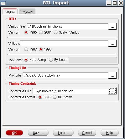
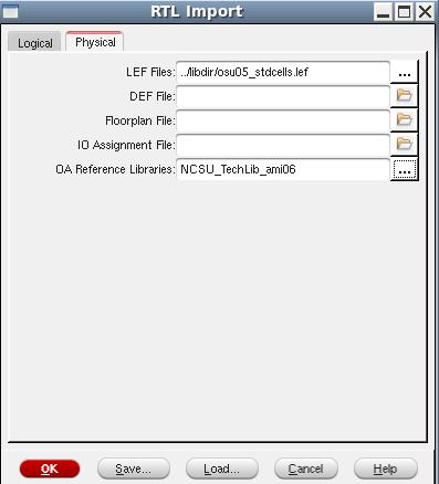
13 Importing Synthesized Verilog Once Encounter is initialized, you need to import your synthesized HDL description file. But first, set the power nets for a later step by typing the following commands in the encounter terminal. set rda_input(ui_pwrnet) {VDD} set rda_input(ui_gndnet) {GND} With that complete, go to File -> Import RTL. Fill in the Verilog Files field with the Verilog files used in the design. Then give a top level name to the design. Under the max timing library field, load the osu05_stdcells.lib. Next, under Timing Constraints, load the SDC file created by RTL Compiler. Move to the Physical tab and load the LEF file for the OSU standard cells called osu05_stdcells.lef which was included in the libdir directory. Finally, in the OA Reference Libraries, add the NCSU_TechLib_ami06 tech library. This will allow the tool to reference the ami06 library for layer information. Click OK and make sure the RTL is successfully imported by looking at the terminal for errors.
14

15 If no errors occur go to File-> Import Design and under Files select../syn/boolean_function_synth.v Do not import the OA under Technology/Physical Libraries, instead clock the LEF Files button and choose../libdir/osu05_stdcells.lef Under Power Nets put VDD and for Ground Nets put GND

16 Floorplanning The Encounter GUI should now display an empty die and the information box in the bottom-right corner should read Design is: In Memory. The next step is to specify a floorplan for your layout. Floorplanning is done to specify the dimensions of your layout and spacing between the core (or area where the standard cells are placed) and power/signal routing. Open up the floorplanning options by clicking on the Floorplan menu and selecting Specify Floorplan. Options that you will need to pay attention to are: Aspect ratio height/width ratio of the core. Suggested: 1.0 (this will change to the closest workable number) Core Utilization the amount of core area used for placing standard cells. A larger value means that your design will be fairly compact but routing may be difficult, if not impossible. Smaller values will drastically increase the design area. Suggested: 0.5 (this will change to the closest workable number) Core Margins by specifies the distance between the core and edge of the die. The margin area needed is proportional to the number of input/output (I/O) pins. Suggested: 10 for core to left, right, top, and bottom Once these values are entered, the layout die/core spacing and aspect ratio should be updated.

17 Power Planning In order to connect your supply voltages to the standard cells, power and ground need to be available on all sides of the die. This is done by adding power rings and specifying global net connections. Select the Power menu and click on Power Planning > Add Rings. A dialog box will pop up and allow you to specify the ring type and configuration. You can plan power in various modes to facilitate various design styles. Since it is preferable to have the routing done inside the power rings, it is a better idea to have them around the I/O boundary so choose this option. If it is not already entered, add GND VDD (without quotes) to the Net(s) field. In the Ring Configuration section, verify that the width and spacing comply with the process design rules and are a multiple of lambda. Once finished, you should see two rings that run inside the I/O boundary. It should look like the following:

18 Connection to the global nets is done automatically if the nets are given the same names as was done in the setting of the power nets above. If all was done correctly, power planning should be finished. Placement Now we are ready to perform the placement. At the end the cells used in the design will be placed so that they don t overlap and there is enough space for routing in between them. Select the Place menu and then Standard Cells. In the dialog box that appears, leave the default settings and hit OK. In the main GUI window, you can verify that the standard cells were placed by selecting the Physical View Icon in the upper-right: You should see the cells placed in the middle of the core. The IO pins have shifted position accordingly as well. If placement fails, it is most likely because Encounter cannot place the cells in the given area without causing gate overlaps. To solve this problem, you must start over by reinitializing the floorplan with relaxed constraints. The best constraint to change is the row utilization factor. By lowering this factor, you can increase the likelihood of placement without overlaps.

19 The final placement should look similar to the following: Routing The built-in routing options within Encounter can now be used to connect the supply nets and create interconnects between the standard cells. Power and ground routing is performed with the Special Route tool. This can be found by selecting the Route menu and then Special Route. In the dialog box that appears, unselect Block pins, Pad pins, and Pad rings. After clicking OK, you should see horizontal and/or vertical metal power routing added to your design. Once power routing is complete, the remaining connections between standard cells and the die I/O can be routed using the NanoRoute tool. Select Route and then NanoRoute and finally Route to enter the dialog box. You do not have to make any changes and can click OK. Your design should now resemble the following:
20 Filler Cells If you import the complete layout from Encounter into Cadence at this point, you may have DRC errors due to nwell layers not being spaced far enough. You can fix these errors by hand in Cadence or you can add pre-designed filler cells with Encounter. These cells provide continuity for nwell layers and power rails between placed cells. Filler cells are placed by selecting the Place menu and then Physcial Cell -> Add Filler. In the dialog box that appears, click Select in the Cell Name(s) field and select the appropriate fill layers. FILLER CELLS IN THE OSU05 LIBRARY ARE JUST CALLED FILL AND THERE IS ONLY ONE OF THEM. You can now click OK to fill in the blank regions in the core of your layout.

21 Verification Before exporting your layout, you need to verify that there are not any geometric errors that occurred during placement or connectivity errors from routing. This can be done by selecting Verify Geometry and Verify Connectivity in the Verify menu. Reports will be generated and placed in the directory that you started Encounter from. You can also look at the terminal used to start Encounter and see the results of the verification. If no errors exist in either geometry or connectivity, the layout is good to fabricate. Save the design by selecting File -> Save Design. This may open to save in OA format, change to encounter format, give it a name and save. GDS Export of Layout from Encounter Once the layout is complete in Encounter (post-routing and post-filler cells), then you need to perform an export of the layout. This is done in Encounter by going to File -> Save -> GDS/OASIS In the window that appears, select the GDSII radio button. Then type an output file name in Output File field such as boolean_function.gds. In the map field select the gds2_encounter.map file located in the libdir directory. In the Library Name, type the Library in Cadence you would like to add the design to. I suggest making up a new library so nothing gets overwritten. Leave all other fields as default making sure the units are 1000 are mode is ALL. Click OK. Look at the terminal and make sure Stream out has finished successfully.
22 Part 4 Import the layout into Cadence. 6. Design in HDL ( Verilog file ) 7. RTL Compiler ( Verilog file --> Synthesized Verilog file ) 8. Encounter ( Synthesized Verilog file --> Layout ) 9. Cadence 3. Layout Import ( Encounter --> CIW Import Stream ) 4. Netlist Import ( Synthesized Verilog file --> Verilog Import ) 10. LVS Verification GDS Import of Layout into Virtuoso After creating a layout in Encounter and creating the GDS file, open Virtuoso. Click on the CIW (Virtuoso window where errors and messages appear) and click File -> Import -> Stream. This may produce an error the first time. Try again and it should work and bring up an import window. On the stream in window choose the GDS file created in Encounter as the Stream In file. Under library, type the name of the library you would like to save the module in. Note, this does need to be the same as the name of the library given in the stream out in Encounter. Then give a name to the top level cell once it is imported.

23 Note: The above assumes you are streaming in to a folder that does not have an attached technology file. If one is attached already do not include anything in the Attach Technology File section. (Also, there is more to do on the next page)
![In the Mapping tab check the Replace [] with](/docs-images/84/90594197/images/24-0.jpg "<> box and Use All Libraries as Ref Lib box.")

24 In the Mapping tab check the Replace [] with <> box and Use All Libraries as Ref Lib box. Finally, Select More Options in the bottom right and go to the Geometry tab. Select Snap To Grid.

25 Now we are ready to translate the file and import the design. Click Translate. If a box to save the libraries comes up make sure to save the libraries as something. The process will take a little bit. When complete there should be a log file and a message box that appears. This should have 0 errors and only a few warnings if not 0. Go to the library created in the Library Manager and try to open the layout of the design. The standard cells should appear. Hit Ctrl+F to see the layout view. Red Cells with no Layers If the cells appear but are red and disappear when you press Shift+F then there is a problem with the technology file in the folder. You should try copying the layout into a library with a known good technology file. If that does not work delete the library and attempt to stream it in again. DRC and LVS error corrections At this point, the synthesized schematic and layout from Encounter have been imported into Virtuoso. DRC will not pass due to dubiousdata errors, the Encounter stream is creating metal layer text that should have been text layer. These can be deleted, but before doing so you should add pins. Encounter is adding the name of what the pin should be where the pin should be placed, but does not actually create the pins. We advise creating the pins with the label name then deleting the label. Congrats on completing this tutorial. Please provide a summary of the steps required for synthesizing and performing layout with Cadence RTL Compiler and SoC Encounter. Explain what the main steps do and provide screen shots of major steps as well as the two verification steps at the end.
26 References Verilog HDL Quick Reference Guide:
EE 330 Laboratory Experiment Number 11 Design and Simulation of Digital Circuits using Hardware Description Languages
 EE 330 Laboratory Experiment Number 11 Design and Simulation of Digital Circuits using Hardware Description Languages Fall 2015 Purpose: The purpose of this experiment is to develop methods for using Hardware
EE 330 Laboratory Experiment Number 11 Design, Simulation and Layout of Digital Circuits using Hardware Description Languages
 EE 330 Laboratory Experiment Number 11 Design, Simulation and Layout of Digital Circuits using Hardware Description Languages Purpose: The purpose of this experiment is to develop methods for using Hardware
Tutorial for Cadence SOC Encounter Place & Route
 Tutorial for Cadence SOC Encounter Place & Route For Encounter RTL-to-GDSII System 13.15 T. Manikas, Southern Methodist University, 3/9/15 Contents 1 Preliminary Setup... 1 1.1 Helpful Hints... 1 2 Starting
Laboratory 6. - Using Encounter for Automatic Place and Route. By Mulong Li, 2013
 CME 342 (VLSI Circuit Design) Laboratory 6 - Using Encounter for Automatic Place and Route By Mulong Li, 2013 Reference: Digital VLSI Chip Design with Cadence and Synopsys CAD Tools, Erik Brunvand Background
Place & Route: Using Silicon Ensemble
 Place & Route: Using Silicon Ensemble Introduction In a typical digital design flow, hardware description language is used to model a design and verify desired behavior. Once the desired functionality
Tutorial for Encounter
 Tutorial for Encounter STEP 1: Login to the Linux system on Linuxlab server. Start a terminal (the shell prompt). (If you don t know how to login to Linuxlab server, look at here) Click here to open a
ECE425: Introduction to VLSI System Design Machine Problem 3 Due: 11:59pm Friday, Dec. 15 th 2017
 ECE425: Introduction to VLSI System Design Machine Problem 3 Due: 11:59pm Friday, Dec. 15 th 2017 In this MP, you will use automated tools to synthesize the controller module from your MP2 project into
EE 330 Spring Laboratory 2: Basic Boolean Circuits
 EE 330 Spring 2013 Laboratory 2: Basic Boolean Circuits Objective: The objective of this experiment is to investigate methods for evaluating the performance of Boolean circuits. Emphasis will be placed
Tutorial 2 Automatic Placement & Routing
 Tutorial 2 Automatic Placement & Routing Please follow the instructions found under Setup on the CADTA main page before starting this tutorial. 1.1. Start Encounter Log on to a VLSI server using your EE
CPE/EE 427, CPE 527, VLSI Design I: Tutorial #4, Standard cell design flow (from verilog to layout, 8-bit accumulator)
") CPE/EE 427, CPE 527, VLSI Design I: Tutorial #4, Standard cell design flow (from verilog to layout, 8-bit accumulator) Joel Wilder, Aleksandar Milenkovic, ECE Dept., The University of Alabama in Huntsville
CPE/EE 427, CPE 527, VLSI Design I: Tutorial #4, Standard cell design flow (from verilog to layout, 8-bit accumulator) Joel Wilder, Aleksandar Milenkovic, ECE Dept., The University of Alabama in Huntsville
VLSI Lab Tutorial 3. Virtuoso Layout Editing Introduction
 VLSI Lab Tutorial 3 Virtuoso Layout Editing Introduction 1.0 Introduction The purpose of this lab tutorial is to guide you through the design process in creating a custom IC layout for your CMOS inverter
Design rule illustrations for the AMI C5N process can be found at:
 Cadence Tutorial B: Layout, DRC, Extraction, and LVS Created for the MSU VLSI program by Professor A. Mason and the AMSaC lab group. Revised by C Young & Waqar A Qureshi -FS08 Document Contents Introduction
Synthesis and APR Tools Tutorial
 Synthesis and APR Tools Tutorial (Last updated: Oct. 26, 2008) Introduction This tutorial will get you familiarized with the design flow of synthesizing and place and routing a Verilog module. All the
Virtuoso Layout Editor
 This tutorial will cover the basic steps involved in using the Cadence layout editor called Virtuoso, extracting layout, and running simulation on the layout. The inverter layout is used as an example
EE 330 Laboratory 3 Layout, DRC, and LVS Fall 2015
 EE 330 Laboratory 3 Layout, DRC, and LVS Fall 2015 Contents Objective:... 2 Part 1 Creating a layout... 2 1.1 Run DRC Early and Often... 2 1.2 Create N active and connect the transistors... 3 1.3 Vias...
and 32 bit for 32 bit. If you don t pay attention to this, there will be unexpected behavior in the ISE software and thing may not work properly!
 This tutorial will show you how to: Part I: Set up a new project in ISE 14.7 Part II: Implement a function using Schematics Part III: Simulate the schematic circuit using ISim Part IV: Constraint, Synthesize,
Physical Placement with Cadence SoCEncounter 7.1
 Physical Placement with Cadence SoCEncounter 7.1 Joachim Rodrigues Department of Electrical and Information Technology Lund University Lund, Sweden November 2008 Address for correspondence: Joachim Rodrigues
EE 330 Spring 2018 Laboratory 2: Basic Boolean Circuits
 EE 330 Spring 2018 Laboratory 2: Basic Boolean Circuits Contents Objective:... 2 Part 1: Introduction... 2 Part 2 Simulation of a CMOS Inverter... 3 Part 2.1 Attaching technology information... 3 Part
EE434 ASIC & Digital Systems. From Layout to SPICE Simulation (Virtuoso, Calibre, HSpice) Spring 2017 Dae Hyun Kim
 Spring 2017 Dae Hyun Kim") EE434 ASIC & Digital Systems From Layout to SPICE Simulation (Virtuoso, Calibre, HSpice) Spring 2017 Dae Hyun Kim daehyun@eecs.wsu.edu 1 Preparation for Lab2 Download the following file into your working
EE434 ASIC & Digital Systems From Layout to SPICE Simulation (Virtuoso, Calibre, HSpice) Spring 2017 Dae Hyun Kim daehyun@eecs.wsu.edu 1 Preparation for Lab2 Download the following file into your working
Revision Notes: July2004 Generate tutorial for single transistor analysis. Based on existing schematic entry tutorial developed for ECE410
 Cadence Analog Tutorial 1: Schematic Entry and Transistor Characterization Created for the MSU VLSI program by Professor A. Mason and the AMSaC lab group. Revision Notes: July2004 Generate tutorial for
Actel Libero TM Integrated Design Environment v2.3 Structural Schematic Flow Design Tutorial
 Actel Libero TM Integrated Design Environment v2.3 Structural Schematic Flow Design Tutorial 1 Table of Contents Design Flow in Libero TM IDE v2.3 Step 1 - Design Creation 3 Step 2 - Design Verification
Cell-Based IC Physical Design & Verification SOC Encounter. Advisor : 李昆忠 Presenter : 蕭智元
 Cell-Based IC Physical Design & Verification SOC Encounter Advisor : 李昆忠 Presenter : 蕭智元 Reference: SOC Encounter Training Manual, 2007, edited by CIC. Introduction We ll use some EDA tools to transform
ESE 570 Cadence Lab Assignment 2: Introduction to Spectre, Manual Layout Drawing and Post Layout Simulation (PLS)
") ESE 570 Cadence Lab Assignment 2: Introduction to Spectre, Manual Layout Drawing and Post Layout Simulation (PLS) Objective Part A: To become acquainted with Spectre (or HSpice) by simulating an inverter,
ESE 570 Cadence Lab Assignment 2: Introduction to Spectre, Manual Layout Drawing and Post Layout Simulation (PLS) Objective Part A: To become acquainted with Spectre (or HSpice) by simulating an inverter,
EE 330 Laboratory 3 Layout, DRC, and LVS
 EE 330 Laboratory 3 Layout, DRC, and LVS Spring 2018 Contents Objective:... 2 Part 1 creating a layout... 2 1.1 Run DRC... 2 1.2 Stick Diagram to Physical Layer... 3 1.3 Bulk Connections... 3 1.4 Pins...
Creating LEF File. Abstract Generation: Creating LEF Tutorial File Release Date: 01/13/2004. Export GDS:
 Creating LEF Tutorial 1-1 - Creating LEF File Abstract Generation: Export GDS: Abstract generator comes as a part of the Silicon Ensemble package. As such, it cannot directly read ICFB library databases.
UNIVERSITY OF CALIFORNIA, DAVIS Department of Electrical and Computer Engineering. EEC180A DIGITAL SYSTEMS I Winter 2015
 UNIVERSITY OF CALIFORNIA, DAVIS Department of Electrical and Computer Engineering EEC180A DIGITAL SYSTEMS I Winter 2015 LAB 1: Introduction to Quartus II Schematic Capture and ModelSim Simulation This
CMOS VLSI Design Lab 3: Controller Design and Verification
 CMOS VLSI Design Lab 3: Controller Design and Verification The controller for your MIPS processor is responsible for generating the signals to the datapath to fetch and execute each instruction. It lacks
Cadence IC Design Manual
 Cadence IC Design Manual For EE5518 ZHENG Huan Qun Lin Long Yang Revised on May 2017 Department of Electrical & Computer Engineering National University of Singapore 1 P age Contents 1 INTRODUCTION...
Cadence SOC Encounter Tutorial for a logic block using the University Of Utah Standard cell Libraries In ON Semiconductor 0.
 Cadence SOC Encounter Tutorial for a logic block using the University Of Utah Standard cell Libraries In ON Semiconductor 0.5 µ C5N CMOS 1. Create a folder called encounter inside of your project folder
UNIVERSITY OF WATERLOO
 UNIVERSITY OF WATERLOO UW ASIC DESIGN TEAM: Cadence Tutorial Description: Part I: Layout & DRC of a CMOS inverter. Part II: Extraction & LVS of a CMOS inverter. Part III: Post-Layout Simulation. The Cadence
EECS 627, Lab Assignment 3
 EECS 627, Lab Assignment 3 1 Introduction In this lab assignment, we will use Cadence ICFB and Calibre to become familiar with the process of DRC/LVS checks on a design. So far, we have placed and routed
EECE 285 VLSI Design. Cadence Tutorial EECE 285 VLSI. By: Kevin Dick Co-author: Jeff Kauppila Co-author: Dr. Arthur Witulski
 Cadence Tutorial EECE 285 VLSI By: Kevin Dick Co-author: Jeff Kauppila Co-author: Dr. Arthur Witulski 1 Table of Contents Purpose of Cadence 1) The Purpose of Cadence pg. 4 Linux 1) The Purpose of Linux
TUTORIAL II ECE 555 / 755 Updated on September 11 th 2006 CADENCE LAYOUT AND PARASITIC EXTRACTION
 TUTORIAL II ECE 555 / 755 Updated on September 11 th 2006 CADENCE LAYOUT AND PARASITIC EXTRACTION After finishing a schematic of your design (Tutorial-I), the next step is creating masks which are for
VLSI Lab Tutorial 1. Cadence Virtuoso Schematic Composer Introduction
 VLSI Lab Tutorial 1 Cadence Virtuoso Schematic Composer Introduction 1.0 Introduction The purpose of the first lab tutorial is to help you become familiar with the schematic editor, Virtuoso Schematic
EE115C Digital Electronic Circuits. Tutorial 4: Schematic-driven Layout (Virtuoso XL)
") EE115C Digital Electronic Circuits Tutorial 4: Schematic-driven Layout (Virtuoso XL) This tutorial will demonstrate schematic-driven layout on the example of a 2-input NAND gate. Simple Layout (that won
EE115C Digital Electronic Circuits Tutorial 4: Schematic-driven Layout (Virtuoso XL) This tutorial will demonstrate schematic-driven layout on the example of a 2-input NAND gate. Simple Layout (that won
An Overview of Standard Cell Based Digital VLSI Design
 An Overview of Standard Cell Based Digital VLSI Design With examples taken from the implementation of the 36-core AsAP1 chip and the 1000-core KiloCore chip Zhiyi Yu, Tinoosh Mohsenin, Aaron Stillmaker,
FACULTY OF ENGINEERING MULTIMEDIA UNIVERSITY LAB SHEET DIGITAL INTEGRATED CIRCUIT
 FACULTY OF ENGINEERING MULTIMEDIA UNIVERSITY LAB SHEET DIGITAL INTEGRATED CIRCUIT DIC1: Schematic Design Entry, Simulation & Verification DIC2: Schematic Driven Layout Drawing (SDL) Design Rule Check (DRC)
CPE/EE 427, CPE 527, VLSI Design I: Tutorial #3, Standard cell design flow (from schematic to layout, 8-bit accumulator)
") CPE/EE 427, CPE 527, VLSI Design I: Tutorial #3, Standard cell design flow (from schematic to layout, 8-bit accumulator) Joel Wilder, Aleksandar Milenkovic, ECE Dept., The University of Alabama in Huntsville
CPE/EE 427, CPE 527, VLSI Design I: Tutorial #3, Standard cell design flow (from schematic to layout, 8-bit accumulator) Joel Wilder, Aleksandar Milenkovic, ECE Dept., The University of Alabama in Huntsville
Cadence Tutorial A: Schematic Entry and Functional Simulation Created for the MSU VLSI program by Andrew Mason and the AMSaC lab group.
 Cadence Tutorial A: Schematic Entry and Functional Simulation Created for the MSU VLSI program by Andrew Mason and the AMSaC lab group. Revision Notes: Aug. 2003 update and edit A. Mason add intro/revision/contents
ECE471/571 Energy Efficient VLSI Design Project 2 Cadence Setup and Creation of an Inverter Due Date 11:30 am on Friday, February 2 nd, 2018
 ECE471/571 Energy Efficient VLSI Design Project 2 Cadence Setup and Creation of an Inverter Due Date 11:30 am on Friday, February 2 nd, 2018 Introduction This project will first walk you through the setup
CMOS VLSI Design Lab 3: Controller Design and Verification
 CMOS VLSI Design Lab 3: Controller Design and Verification The controller for your MIPS processor is responsible for generating the signals to the datapath to fetch and execute each instruction. It lacks
The IIT standard cell library Version 2.1
 The IIT standard cell library Version 2.1 Highlights - Support for AMI 0.35um library, including pads - Added Primetime and Pathmill support to IIT ASIC Flow - Support for stacked vias (for Virtuoso and
Cadence Tutorial 2: Layout, DRC/LVS and Circuit Simulation with Extracted Parasitics
 Cadence Tutorial 2: Layout, DRC/LVS and Circuit Simulation with Extracted Parasitics Introduction This tutorial describes how to generate a mask layout in the Cadence Virtuoso Layout Editor. Use of DIVA
ASIC Physical Design Top-Level Chip Layout
 ASIC Physical Design Top-Level Chip Layout References: M. Smith, Application Specific Integrated Circuits, Chap. 16 Cadence Virtuoso User Manual Top-level IC design process Typically done before individual
EE 330 Fall 2017 Lab 1: Cadence Custom IC design tools - Setup, Schematic capture and simulation
 EE 330 Fall 2017 Lab 1: Cadence Custom IC design tools - Setup, Schematic capture and simulation Table of Contents Objective... 2 1. Setup... 2 Set Bash Shell for the account... 2 2. Starting Cadence Custom
EE 330 Spring 2018 Lab 1: Cadence Custom IC design tools Setup, Schematic capture and simulation
 EE 330 Spring 2018 Lab 1: Cadence Custom IC design tools Setup, Schematic capture and simulation Table of Contents Objective... 2 1. Setup... 2 Set Bash Shell for the account... 2 2. Starting Cadence Custom
CPE/EE 427, CPE 527, VLSI Design I: Tutorial #2, Schematic Capture, DC Analysis, Transient Analysis (Inverter, NAND2)
") CPE/EE 427, CPE 527, VLSI Design I: Tutorial #2, Schematic Capture, DC Analysis, Transient Analysis (Inverter, NAND2) Joel Wilder, Aleksandar Milenkovic, ECE Dept., The University of Alabama in Huntsville
CPE/EE 427, CPE 527, VLSI Design I: Tutorial #2, Schematic Capture, DC Analysis, Transient Analysis (Inverter, NAND2) Joel Wilder, Aleksandar Milenkovic, ECE Dept., The University of Alabama in Huntsville
Cadence On-Line Document
 Cadence On-Line Document 1 Purpose: Use Cadence On-Line Document to look up command/syntax in SoC Encounter. 2 Cadence On-Line Document An on-line searching system which can be used to inquire about LEF/DEF
Select the technology library: NCSU_TechLib_ami06, then press OK.
 ECE 126 Inverter Tutorial: Schematic & Symbol Creation Created for GWU by Anis Nurashikin Nordin & Thomas Farmer Tutorial adapted from: http://www.ee.ttu.edu/ee/cadence/commondirectory/final%20tutorials/digitalcircuitsimulationusingvirtuoso.doc
UNIVERSITY OF CALIFORNIA College of Engineering Department of Electrical Engineering and Computer Sciences Lab #2: Layout and Simulation
 UNIVERSITY OF CALIFORNIA College of Engineering Department of Electrical Engineering and Computer Sciences Lab #2: Layout and Simulation NTU IC541CA 1 Assumed Knowledge This lab assumes use of the Electric
Lab 1: Cadence Custom IC design tools- Setup, Schematic capture and simulation
 Lab 1: Cadence Custom IC design tools- Setup, Schematic capture and simulation Brittany Duffy EE 330- Integrated Electronics Lab Section B Professor Randy Geiger 1/24/13 Introduction The main goal of this
CADENCE TUTORIAL. San Diego State University, Department of Electrical and Computer Engineering. Amith Dharwadkar and Ashkan Ashrafi
 CADENCE TUTORIAL San Diego State University, Department of Electrical and Computer Engineering Amith Dharwadkar and Ashkan Ashrafi 1 Contents 1) 2) 3) 4) 5) 6) Introduction 3 Connecting to the Volta server..4
An overview of standard cell based digital VLSI design
 An overview of standard cell based digital VLSI design Implementation of the first generation AsAP processor Zhiyi Yu and Tinoosh Mohsenin VCL Laboratory UC Davis Outline Overview of standard cellbased
CMOS Design Lab Manual
 CMOS Design Lab Manual Developed By University Program Team CoreEl Technologies (I) Pvt. Ltd. 1 Objective Objective of this lab is to learn the Mentor Graphics HEP2 tools as well learn the flow of the
Tutorial I: Cadence Innovus ECE6133: Physical Design Automation of VLSI Systems Georgia Institute of Technology Prof. Sung Kyu Lim
 Tutorial I: Cadence Innovus ECE6133: Physical Design Automation of VLSI Systems Georgia Institute of Technology Prof. Sung Kyu Lim I. Setup for Cadence Innovus 1. Copy the following files into your working
DRC and LVS checks using Cadence Virtuoso Version 3.0
 DRC and LVS checks using Cadence Virtuoso Version 3.0 Start virtuoso l l Open a virtuoso session in the directory which contains the required cds.lib and lib.def files. Command : virtuoso & Open the layout
Abstract Editor (Last updated: Oct. 23, 2008)
") Abstract Editor (Last updated: Oct. 23, 2008) Abstract Editor Tutorial This tutorial has been created to discuss all of the steps needed to create an abstract Library Exchange Format (LEF) file for custom
Abstract Editor (Last updated: Oct. 23, 2008) Abstract Editor Tutorial This tutorial has been created to discuss all of the steps needed to create an abstract Library Exchange Format (LEF) file for custom
CMOS VLSI Design Lab 3: Controller Design and Verification
 CMOS VLSI Design Lab 3: Controller Design and Verification The controller for your MIPS processor is responsible for generating the signals to the datapath to fetch and execute each instruction. It lacks
AMS 0.18 µm PDK Setup and Cadence Tutorial Contributors
 AMS 0.18 µm PDK Setup and Cadence Tutorial Contributors Muhammad Ahmed, Sita Asar, and Ayman Fayed, Power Management Research Lab, https://pmrl.osu.edu, Department of Electrical and Computer Engineering,
Microelectronica. Full-Custom Design with Cadence Tutorial
 Área Científica de Electrónica Microelectronica Full-Custom Design with Cadence Tutorial AustriaMicroSystems C35B3 (HIT-Kit 3.70) Marcelino Santos Table of contends 1. Starting Cadence... 3 Starting Cadence
CPE/EE 427, CPE 527, VLSI Design I: Tutorial #1, Full Custom VLSI (inverter layout)
") CPE/EE 427, CPE 527, VLSI Design I: Tutorial #1, Full Custom VLSI (inverter layout) Joel Wilder, Aleksandar Milenkovic, ECE Dept., The University of Alabama in Huntsville Adapted from Virginia Tech, Dept.
CPE/EE 427, CPE 527, VLSI Design I: Tutorial #1, Full Custom VLSI (inverter layout) Joel Wilder, Aleksandar Milenkovic, ECE Dept., The University of Alabama in Huntsville Adapted from Virginia Tech, Dept.
CS 4120 Hardware Description Languages and Synthesis Homework 6: Introduction to Cadence Silicon Ensemble
 CS 4120 Hardware Description Languages and Synthesis Homework 6: Introduction to Cadence Silicon Ensemble 0. Introduction In this homework, you will be introduced to a Place and Route tool called Silicon
CS755 CAD TOOL TUTORIAL
 CS755 CAD TOOL TUTORIAL CREATING SCHEMATIC IN CADENCE Shi-Ting Zhou shi-ting@cs.wisc.edu After you have figured out what you want to design, and drafted some pictures and diagrams, it s time to input schematics
ANALOG MICROELECTRONICS ( A)
") ANALOG MICROELECTRONICS (304-534A) IBM 130 nm CMOS Technology An Introduction to Cadence Virtuoso Layout Tool and the Analog Simulation Environment Prepared By - Azhar A. Chowdhury Updated by Ming Yang
ANALOG MICROELECTRONICS (304-534A) IBM 130 nm CMOS Technology An Introduction to Cadence Virtuoso Layout Tool and the Analog Simulation Environment Prepared By - Azhar A. Chowdhury Updated by Ming Yang
Lab. Course Goals. Topics. What is VLSI design? What is an integrated circuit? VLSI Design Cycle. VLSI Design Automation
 Course Goals Lab Understand key components in VLSI designs Become familiar with design tools (Cadence) Understand design flows Understand behavioral, structural, and physical specifications Be able to
CPE/EE 427, CPE 527, VLSI Design I: Tutorial #3, Standard cell design flow (from schematic to layout, 8-bit accumulator)
") CPE/EE 427, CPE 527, VLSI Design I: Tutorial #3, Standard cell design flow (from schematic to layout, 8-bit accumulator) Joel Wilder, Aleksandar Milenkovic, ECE Dept., The University of Alabama in Huntsville
CPE/EE 427, CPE 527, VLSI Design I: Tutorial #3, Standard cell design flow (from schematic to layout, 8-bit accumulator) Joel Wilder, Aleksandar Milenkovic, ECE Dept., The University of Alabama in Huntsville
Virtuoso Schematic Composer
 is a schematic design tool from Cadence. In this tutorial you will learn how to put electrical components, make wire connections, insert pins and check for connection error. Start Cadence Custom IC Design
HOMEWORK 9 CMPEN 411 Due: 4/12/ :30pm
 HOMEWORK 9 CMPEN 411 Due: 4/12/2016 11:30pm Learning Objective Complete the full 8 bit RISC microprocessor chip design by placing the processor core design into the 40 pin 'tiny' chip pad frame. Do verify
EEC 116 Fall 2011 Lab #1 Cadence Schematic Capture and Layout Tutorial
 EEC 116 Fall 2011 Lab #1 Cadence Schematic Capture and Layout Tutorial Dept. of Electrical and Computer Engineering University of California, Davis September 26, 2011 Reading: Rabaey Chapters 1, 2, A,
Pipelined MIPS CPU Synthesis and On-Die Representation ECE472 Joseph Crop Stewart Myers
 Pipelined MIPS CPU Synthesis and On-Die Representation ECE472 Joseph Crop Stewart Myers 2008 Table of Contents Introduction... 3 Steps Taken and Simulation... 3 Pitfalls... 8 Simulated Delay... 9 APPENDIX
Tutorial: Working with the Xilinx tools 14.4
 Tutorial: Working with the Xilinx tools 14.4 This tutorial will show you how to: Part I: Set up a new project in ISE Part II: Implement a function using Schematics Part III: Implement a function using
INTRODUCTION TO MENTOR GRAPHICS DESIGN TOOLS
 INTRODUCTION TO MENTOR GRAPHICS DESIGN TOOLS 1. RUNNING MENTOR GRAPHICS Erdem S. Erdogan 09.13.2006 Note: These commands can be run remotely via ssh to one of the DSIL machines. If running remotely, ignore
Cell-Based Design Flow. TA : 吳廸優
 Cell-Based Design Flow TA : 吳廸優 dywu@viplab.cs.nctu.edu.tw 1 Outline Overview Design Flow Stage 1 RTL Development Synthesis Gate Level Simulation Design Flow Stage 2 Placement and Routing Post Layout Simulation
EE183 LAB TUTORIAL. Introduction. Projects. Design Entry
 EE183 LAB TUTORIAL Introduction You will be using several CAD tools to implement your designs in EE183. The purpose of this lab tutorial is to introduce you to the tools that you will be using, Xilinx
Lab 1 Modular Design and Testbench Simulation ENGIN 341 Advanced Digital Design University of Massachusetts Boston
 Lab 1 Modular Design and Testbench Simulation ENGIN 341 Advanced Digital Design University of Massachusetts Boston Introduction This lab introduces the concept of modular design by guiding you through
CMOS VLSI Design Lab 4: Full Chip Assembly
 CMOS VLSI Design Lab 4: Full Chip Assembly In this final lab, you will assemble and simulate your entire MIPS microprocessor! You will build your top level chip cell by connecting the datapath, aludec,
Start Active-HDL. Create a new workspace TUTORIAL #1 CREATING AND SIMULATING SIMPLE SCHEMATICS
 Introduction to Active-HDL TUTORIAL #1 CREATING AND SIMULATING SIMPLE SCHEMATICS This tutorial will introduce the tools and techniques necessary to design a basic schematic. The goal of this tutorial is
Creating Verilog Tutorial Netlist Release Date: 01/13/2005(Version 2)
") Creating Verilog Tutorial 2-1 - Creating a verilog netlist for a schematic: The verilog netlist is necessary for automatic layout (placement and routing) tools. It contains information about the I/O pins
Creating Verilog Tutorial 2-1 - Creating a verilog netlist for a schematic: The verilog netlist is necessary for automatic layout (placement and routing) tools. It contains information about the I/O pins
Cadence Tutorial: Schematic Entry and Circuit Simulation of a CMOS Inverter
 Cadence Tutorial: Schematic Entry and Circuit Simulation of a CMOS Inverter Introduction This tutorial describes the steps involved in the design and simulation of a CMOS inverter using the Cadence Virtuoso
DRC and LVS checks using Cadence Virtuoso Version 2.0
 DRC and LVS checks using Cadence Virtuoso Version 2.0 Start virtuoso l l Open a virtuoso session in the directory which contains the required cds.lib and lib.def files. Command : virtuoso & Open the layout
Cadence Virtuoso Schematic Design and Circuit Simulation Tutorial
 Cadence Virtuoso Schematic Design and Circuit Simulation Tutorial Introduction This tutorial is an introduction to schematic capture and circuit simulation for ENGN1600 using Cadence Virtuoso. These courses
Outline. SoC Encounter Flow. Typical Backend Design Flow. Digital IC-Project and Verification. Place and Route. Backend ASIC Design flow
 Outline Digital IC-Project and Verification Deepak Dasalukunte Backend ASIC Design flow General steps Input files Floorplanning Placement Clock-synthesis Routing Typical Backend Design Flow SoC Encounter
This is a brief tutorial about building a Symbol for a Schematic in Cadence IC design tool environment for hierarchical design of schematics.
 This is a brief tutorial about building a Symbol for a Schematic in Cadence IC design tool environment for hierarchical design of schematics. 1. > cd work035 2. > cadsetup ams035 3. > virtuoso& IMPORTANT:
Hardware Verification Group. Department of Electrical and Computer Engineering, Concordia University, Montreal, Canada. CAD Tool Tutorial.
 Digital Logic Synthesis and Equivalence Checking Tools Hardware Verification Group Department of Electrical and Computer Engineering, Concordia University, Montreal, Canada CAD Tool Tutorial May, 2010
ECE 425: Introduction to VLSI System Design Machine Problem 0 Due: Friday 11:59pm, Sep. 15th, 2017
 ECE 425: Introduction to VLSI System Design Machine Problem 0 Due: Friday 11:59pm, Sep. 15th, 2017 You will spend most of your lab time using the Virtuoso design tools from Cadence Design Systems. Virtuoso
CPEN 230L: Introduction to Digital Logic Laboratory Lab #6: Verilog and ModelSim
 CPEN 230L: Introduction to Digital Logic Laboratory Lab #6: Verilog and ModelSim Purpose Define logic expressions in Verilog using register transfer level (RTL) and structural models. Use Quartus II to
Vivado Design Suite User Guide
 Vivado Design Suite User Guide Design Flows Overview Notice of Disclaimer The information disclosed to you hereunder (the Materials ) is provided solely for the selection and use of Xilinx products. To
Graphics: Alexandra Nolte, Gesine Marwedel, Universität Dortmund. RTL Synthesis
 Graphics: Alexandra Nolte, Gesine Marwedel, 2003 Universität Dortmund RTL Synthesis Purpose of HDLs Purpose of Hardware Description Languages: Capture design in Register Transfer Language form i.e. All
The original document link is
 Tutorial:Analog Artist with HSPICE The original document link is http://www.eda.ncsu.edu/wiki/tutorial:analog_artist_with_hspice This tutorial will introduce you to the Cadence Environment: specifically
Synopsys Custom Designer Tutorial for a chip integra7on using the University of Utah Standard Cell Libraries In ON Semiconductor 0.
 Synopsys Custom Designer Tutorial for a chip integra7on using the University of Utah Standard Cell Libraries In ON Semiconductor 0.5u C5 CMOS Version 6.0 Overview This tutorial will take you through the
CPE/EE 427, CPE 527, VLSI Design I: VHDL design simulation, synthesis, and ASIC flow, Laboratory #8,
 CPE/EE 427, CPE 527, VLSI Design I: VHDL design simulation, synthesis, and ASIC flow, Laboratory #8, Joel Wilder and Aleksandar Milenkovic, ECE Dept., The University of Alabama in Huntsville 1. INTRODUCTION
EECS 627, Lab Assignment 2
 EECS 627, Lab Assignment 2 1 Introduction In this lab assignment, you will extend the process of designing your multiplier chip. You will add two more blocks (a pseudo-random test pattern generator and
More information can be found in the Cadence manuals Virtuoso Layout Editor User Guide and Cadence Hierarchy Editor User Guide.
 Chapter 6 Building with Layout This chapter consists of two parts. The first describes the generation of layout views and the second deals with the various tools used for verifying the layout, both physical
Logic synthesis and Place and Route Tutorial Page 1
 Logic synthesis and Place and Route Tutorial Page 1 Standard Cell ASIC Design flow: A designer uses predesigned logic cells such as AND gate, NOR gate, etc. These gates are called Standard Cells. The advantage
Another view of the standard cells called the abstract view needs to generated
 Abstract Generation Place and route tools do not require the full cell layout Another view of the standard cells called the abstract view needs to generated The abstract view provides information like:
DOWNLOAD PDF CADENCE WAVEFORM CALCULATOR USER GUIDE
 Chapter 1 : CSE / Cadence Tutorial The Cadence Design Communities support Cadence users and technologists interacting to exchange ideas, news, technical information, and best practices to solve problems
Digital IC- Project 1. Place and Route. Oskar Andersson. Oskar Andersson, EIT, LTH, Digital IC project and Verifica=on
 Digital IC- Project 1 Oskar Andersson Outline Backend ASIC Design flow (Physical Design) General steps Input files Floorplanning Placement ClockTree- synthesis Rou=ng Typical Backend Design Flow Synthesis
Verilog Design Entry, Synthesis, and Behavioral Simulation
 ------------------------------------------------------------- PURPOSE - This lab will present a brief overview of a typical design flow and then will start to walk you through some typical tasks and familiarize
PlanAhead Software Tutorial
 PlanAhead Software Tutorial RTL Design and IP Generation The information disclosed to you hereunder (the Information ) is provided AS-IS with no warranty of any kind, express or implied. Xilinx does not
CS/EE 5720/6720 Analog IC Design Tutorial for Schematic Design and Analysis using Spectre
 CS/EE 5720/6720 Analog IC Design Tutorial for Schematic Design and Analysis using Spectre Introduction to Cadence EDA: The Cadence toolset is a complete microchip EDA (Electronic Design Automation) system,