NanoLens AFM and Bruker 3D Microscopes Integrated 1000X Inspection Combines for Maximum Metrology Value
|
|
|
- Frederica Poole
- 6 years ago
- Views:
Transcription

1 NanoLens AFM and Bruker 3D Microscopes Integrated 1000X Inspection Combines for Maximum Metrology Value
2 Outline Introduction/Administrative Overview of Bruker 3D Optical Microscopes Software, Automation Ease of Use Functionality Overview of NanoLens AFM module 1000X Lens Defect Inspection Example Summary/Q&A 2


3 Introduction Bruker Nano Surfaces Division Widest selection of metrology and tribology platforms Only major AFM manufacturer with world-class probes nanofabrication World leader in innovation -- over 180 patents in AFM, stylus and optical metrology Tribology and Mechanical Testing Nano/microscale wear, indentation, frictional analysis of materials Atomic Force Microscopy Nanoscale characterization of compositional and material properties 3D Optical Microscopy Non-contact 3D measurement of surface texture and roughness Stylus Profiling Measure thin film roughness, step heights and stress 3


4 Introduction Bruker Nano Surfaces Division Stylus and Optical Metrology Technology Leadership 60+ Patents 3 R&D 100 Awards 6 Photonics Circle of Excellence Awards Manufacturing Excellence Lean, six sigma-based process >100 systems/quarter capacity Rapid production ramp capability 4
 Industry experience (16+ years) optical engineering, fabrication and metrology Earned Ph.D.")
5 Introduction Speaker Background Matt Novak, Ph.D. Manager, SOM Applications Development Bruker Corporation Nano Surfaces Division Applications at Bruker (2+ years) Industry experience (16+ years) optical engineering, fabrication and metrology Earned Ph.D. working in private sector metrology capital equipment 5


6 Who Will Benefit? Intended Webinar Audience Technicians, engineers, and researchers interested in 3D optical microscopes Those interested in automated inspection capabilities Those interested in highest resolution metrology available for critical failure analysis and quality assurance needs People interested in AFM imaging, automation for ease of use, as well as 3D optical inspection for QA/QC, failure analysis, and process control 6
7 Why 3D Optical Microscopes? Value Delivery for Precision Applications Capital metrology equipment protects investment of Money Time Productivity Bruker 3D Microscopes Deliver Tremendous Value and Savings Across These Elements Equipment Materials Operators Machining Capital Employment Rework Reduction 7


8 Value from Webinar After the Presentation You Will Understand the value of Bruker s 3D microscopes for metrology across a range of applications Automation and ease of use capabilities Understand the value of integrated AFM capability on Bruker s 3D microscope platforms for high resolution metrology applications Survey responses appreciated 8
9 Outline Introduction/Administrative Overview of Bruker 3D Optical Microscopes Advantages in Software, Automation Ease of Use, Functionality Overview of NanoLens AFM module 1000X Lens Defect Inspection Example Summary/Q&A 9


10 Bruker 3D Optical Microscopes Produce 3D Images of Area of Interest Microscopes with special objectives used to provide sample height data Optics scanned vertically so that sample is passed through focus Computer system computes height information from this focus scan data 10


11 Bruker 3D Optical Microscopes Metrology for Broad Applications Excellent vertical resolution combined with high lateral resolution for large area metrology 11


12 Bruker 3D Optical Microscopes Metrology for Broad Applications Metals Life Sciences MEMS (MicroElectroMechanical Systems) Semiconductors Optics Materials 12

13 Advantages of Bruker 3D Microscopes Truly Universal VXI for Ease of Use VXI Universal mode, for any stepped, smooth or rough surface VXI uses complete optical signal for optimum results VXI renders topography by Self-sensing smooth/rough surface Producing highest quality data on smooth surfaces Reducing noise and artifacts on rougher surfaces 15 nm S a Surface 13

14 Advantages of Bruker 3D Microscopes Excellent Repeatability, All Magnifications Bruker 3D microscopes measure at both high magnification and low magnification with Highest Performance in Repeatability 5/8/


15 Advantages of Bruker 3D Microscopes Multi-grid Automation for Ease of Use Multi-grid automation Supports multiple measurements per die or region (trays, etc.) Simple setup, fast! 15

16 Advantages of Bruker 3D Microscopes COGNEX Pattern Alignment Automated alignment with COGNEX Fast! bright field image recipes supported Operator independent Teach patterns inside Vision64 totally integrated solution! Critical for SEMI, automotive, micro machining, MEMS sensors and other apps 16


17 Advantages of Bruker 3D Microscopes Imaging and Metrology Combined! Sharp Images, Fastest Time to Data are Key Advantages 17

18 Advantages of Bruker 3D Microscopes Ease of Display and Output Customization 18

19 Advantages of Bruker 3D Microscopes Fastest Time to Data Bruker 3D Microscopes Deliver Fast Image Acquisition Single Measurement Location Scanner Speed 100+ Auto Scan Return Real-time Auto Intensity Multiple Locations Measurement Scanner Speed Auto Scan Return, Tilt Adjust Real time Auto Intensity Easy XY Automation Stitching Auto Scan Return High Speed Auto Focus SPEED = Image Acquisition + Data Analysis 19

20 Advantages of Bruker 3D Microscopes Automated Tip/Tilt of Optical Head Auto tip/tilt achieves Better repeatability Better reproducibility Fastest time to data on long scans Simple set up! Enables following of surface for shortest possible scans 20


21 Advantages of Bruker 3D Microscopes Automated Tip/Tilt of Optical Head Tip/tilt head enables auto adjust of tilt User sets controls for desired alignment condition System measures and adjusts automatically for tilt Allows sample tracking and shortest scan lengths on large warped/bowed samples 21


22 Advantages of Bruker 3D Microscopes Automatic Region ID and Coordinate Maps Time to Data Advantage: Multiple Region Analysis Multiple Regions, Log Data and COORDINATES Multiple Multiple Regions, Analyze in One Image Acquisition Automatic Region ID, Data and Statistics without operator intervention SPEED = Image Acquisition + Data Analysis 5/8/
23 Outline Introduction/Administrative Overview of Bruker 3D Optical Microscopes Software, Automation Ease of Use Functionality Overview of NanoLens AFM module 1000X Lens Defect Inspection Example Summary/Q&A 23

24 ContourGT and NanoLens AFM Excellent 3D Microscope Metrology and 1000X AFM Lens in Single System 24

25 Bruker s NanoLens AFM Why 1000X? Highest Turret Magnification! Approximate 200x FOV 1000X Image easily achieved by NanoLens AFM! 25 µm 5 µm 25 µm 5 µm 25


26 Bruker ContourGT + NanoLens AFM Value-Added Metrology Solution World s only 3D optical microscopes with integrated AFM module operated from system software AND backed by extensive WW AFM expertise Ideal combination for DEFECT REVIEW applications requiring low magnification ID, high resolution measurement Integrated ON PLATFORM capability saves process, load and unload time maximizes operator productivity 26


27 NanoLens AFM Module Specs General Technical Specs for Module Simple Cantilever Mounting System 27

28 NanoLens AFM Microscope Integration Features and Benefits to Applications Parcentric AFM to 50x FOV within ~ 15 µm Integrated 8X optical objective for observation Identify areas of interest to inspect via optical or AFM On-board AFM enables fastest time to data for FA or QA labs, among other uses Standard sample image at 16X magnification 28
 Defect/Contamination Review NanoLens AFM for highest resolution!")
29 ContourGT + NanoLens AFM Bringing the Power of AFM to Bruker 3D Microscopes Applications include On-board verification of highest resolution measurements Thin film steps Dissimilar materials, smooth surfaces (semi wafer apps, MEMS, lithography, etc.) Defect/Contamination Review NanoLens AFM for highest resolution! 29
30 Outline Introduction/Administrative Overview of Bruker 3D Optical Microscopes Software, Automation Ease of Use Functionality Overview of NanoLens AFM module 1000X Lens Defect Inspection Example Summary/Q&A 30
31 Bruker 3D Microscope + NanoLens AFM Defect/Contamination Review Application 3D microscope measurements indicate areas of interest for higher magnification inspection Result of multiple measurement sites from automation run and saved data coordinates (AUTO Region ID from multiple regions) Stage auto locates measurement locations for highest resolution inspection Parcentric NanoLens AFM images sample areas and provide highest resolution results all ON SAME platform! 31

32 ContourGT + NanoLens AFM Wafer Inspection Application Sample for inspection HB LED wafer in process Wafer inspection - use ContourGT to inspect levels of LED structure and mesa, fingers at low magnification Low magnification ID coordinates stage import for defect review NanoLens AFM can provide additional insight to detailed structures 32


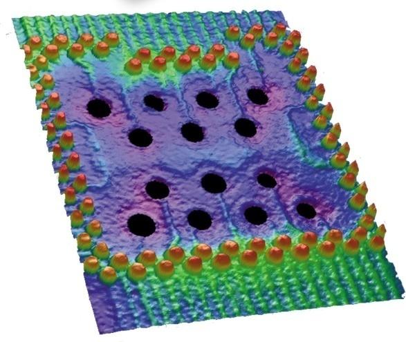
33 ContourGT + NanoLens AFM Defect/Contamination Review Application Low magnification inspection identifies defect - 100X image reveals pitting 33

34 ContourGT + NanoLens AFM Defect/Contamination Review Application Optical inspection shows ~ 1 micron tall, ~ 1 micron wide bump - which is it? Confirm via NanoLens AFM 34

35 ContourGT + NanoLens AFM Defect/Contamination Review Application NanoLens AFM Easily Confirms Nature of Defect 35
36 Outline Introduction/Administrative Overview of Bruker 3D Optical Microscopes Software, Automation Ease of Use Functionality Overview of NanoLens AFM module 1000x Lens Defect Inspection Example Summary/Q&A 36
37 Summary Introduced Bruker BNS, Bruker 3D Optical Microscopes and their advantages for metrology, speed and ease of use Introduced Bruker s NanoLens AFM and covered the combined 3D Optical Microscope value-add for this capability Outlined an application for on-board 1000X imaging for a simple defect review example Questions open any unanswered will be followed up via when yours is linked to your company name 37
38 Summary Presenter Contact: Questions? 38


39 Copyright Bruker Corporation. All rights reserved.
Mobility and Miniaturization 3D WLI Microscopes Address Key Metrology Needs
 Mobility and Miniaturization 3D WLI Microscopes Address Key Metrology Needs Outline Introductions Brief Overview of 3D Microscopes based on WLI General technology description Benefits and general applications
Application Note #554 VXI Universal Surface Measurements for 3D Optical Microscopes
 Surface detail of smooth AMOLED substrate Detail of LED wafer and interactive cursors Application Note #554 VXI Universal Surface Measurements for 3D Optical Microscopes MEMS inertial sensor Bruker has
Discover 3D measurements for flexible electronics: a metrology masterclass
 Discover 3D measurements for flexible electronics: a metrology masterclass Samuel Lesko Bruker Nano Surfaces 21 November 2013 Smithers Pira the worldwide authority on the packaging, paper and print industry
Contour LS-K Optical Surface Profiler
 Contour LS-K Optical Surface Profiler LightSpeed Focus Variation Provides High-Speed Metrology without Compromise Innovation with Integrity Optical & Stylus Metrology Deeper Understanding More Quickly
Sample study by 3D optical profiler Contour Elite K for KTH university.
 Sample study by 3D optical profiler Contour Elite K for KTH university Samuel.lesko@bruker.com Objectives Objectives Main goals for the visit consist of evaluating 3D optical profiler: Confirm capability
ZEISS Smartproof 5 Your Integrated Widefield Confocal Microscope for Surface Analysis in Quality Assurance and Quality Control
 Product Information Version 1.0 ZEISS Smartproof 5 Your Integrated Widefield Confocal Microscope for Surface Analysis in Quality Assurance and Quality Control Dedicated Design. Guided Workflow. Trusted
3D Scratch Tester. 3D Profilometer. Scratch Tester. Fully Automated. Nano, Micro and Macro Range
 3D Scratch Tester Thin Film/ Coating Adhesion, Scratch Resistance, Hardness Wear, Roughness, Film Thickness, Sub-Nanometer Topograph Scratch Tester + 3D Profilometer Fully Automated Nano, Micro and Macro
AUTOFOCUS SENSORS & MICROSCOPY AUTOMATION IR LASER SCANNING CONFOCAL MICROSCOPE IRLC DEEP SEE. Now See Deeper than ever before
 AUTOFOCUS SENSORS & MICROSCOPY AUTOMATION IR LASER SCANNING CONFOCAL MICROSCOPE IRLC DEEP SEE Now See Deeper than ever before Review and inspection of non visible subsurface defects Non visible and subsurface
Advances in Disk Metrology
 Advances in Disk Metrology Robert Kertayasa Zeta Instruments March 2011 www.zeta-inst.com 1909 Concourse Drive San Jose CA 95131 PHONE (408) 577-1888 FAX (408) 577-0588 Agenda Introduction Technology Sample
Advantages of 3D Optical Profiling Over Other Measurement Technologies
 Horizontal milling Ra (6.35 μm, 250 uin.) Vertical milling Ra (1.6 μm, 63 uin.) Flat lapping Ra (0.2 μm, 8 uin.) Application Note #558 Correlating Advanced 3D Optical Profiling Surface Measurements to
DEKTAK XT MECHANICAL PROFILOMETER
 EPFL STI CMi DEKTAK XT MECHANICAL PROFILOMETER The DektakXT stylus surface profiler is an advanced thin and thick film step height measurement tool with the following characteristics: - equipment compatible
SPECTRUM. The world s first fully automated Raman AFM. AFM - confocal Raman - SNOM - TERS AFM KPFM. Raman. AFM-Raman characterization of PS-PVAC
 Raman KPFM AFM AFM-Raman characterization of PS-PVAC polymer blend film SPECTRUM The world s first fully automated Raman AFM AFM - confocal Raman - SNOM - TERS The first fully integrated & automated AFM
Precise flatness measurement
 NEW Simple Roughness and flatness in one measurement Reliable Measurement of step heights High Precision Measurements down to the nanometer range Safe Accuracy in deep layers Efficient Semi-automatic series
Bringing Patterned Media to Production with Value Added Metrology
 Bringing Patterned Media to Production with Value Added Dean Dawson, Andrew S. Lopez Diskcon /IDEMA Conference, Session 6 September 24th, 2009 Overview Introduction AFM Scan Modes New Nanotrench Pattern
Opto-digital microscopy The future of industrial quality control
 Opto-digital microscopy The future of industrial quality control Abstract: Industrial quality assessment tasks Function often relates to form, and this holds particular truth within the world of manufacturing.
ZEISS Launches New High-resolution 3D X-ray Imaging Solutions for Advanced Semiconductor Packaging Failure Analysis
 Press Release ZEISS Launches New High-resolution 3D X-ray Imaging Solutions for Advanced Semiconductor Packaging Failure Analysis New submicron and nanoscale XRM systems and new microct system provide
Phenom TM Pro Suite. The ultimate application software solution. Specification Sheet
 Phenom TM Pro Suite The ultimate application software solution The Phenom TM Pro Suite is developed to enable Phenom users to extract maximum information from images made with the Phenom G2 pro desktop
Jr25 OPTICAL OPTIONS. 20 x 30 x 17 cm
 PROFILOMETERS Nanovea Profilometers are designed with leading edge Chromatic Confocal optical technology (axial chromatism) both ISO and ASTM compliant. The technique measures a physical wavelength directly
PLASTIC FILM TEXTURE MEASUREMENT USING 3D PROFILOMETRY
 PLASTIC FILM TEXTURE MEASUREMENT USING 3D PROFILOMETRY Prepared by Jorge Ramirez 6 Morgan, Ste156, Irvine CA 92618 P: 949.461.9292 F: 949.461.9232 nanovea.com Today's standard for tomorrow's materials.
SUSS MJB4. Manual Aligner For Research, Development and Operator Assisted Production October, 2009
 SUSS MJB4 Manual Aligner For Research, Development and Operator Assisted Production October, 2009 Overview Product Portfolio Aligner MA/BA 8 MA200Compact LithoFab200 MJB4 MA300Plus MA/BA 6 MA150e LithoPack300
3D Surface Analysis Form & Roughness Measurement Automatic Depth Composition Z Depth Measurement
 MICROSCOPE 3D ADD ON FAST PRECISE AFFORDABLE 3D ADD ON FOR MICROSCOPES 3D Surface Analysis Form & Roughness Measurement Automatic Depth Composition Z Depth Measurement Compatible With Compound Microscopes
EMPIR Grant Agreement 14IND07 3D Stack
 EMPIR Grant Agreement 14IND07 3D Stack Good Practice Guide: Recommendations on the strategy for measuring the dimensional properties of TSVs based on Confocal microscopy, IR interferometry and optical
Compact 3D optical surface profiler
 Compact 3D optical surface profiler Compact. Flexible. Powerful. S lynx is a new non-contact 3D surface profiler designed for use in industry and research. It has been designed as a compact and versatile
O-RING SURFACE INSPECTION USING 3D PROFILOMETRY
 O-RING SURFACE INSPECTION USING 3D PROFILOMETRY Prepared by Jorge Ramirez 6 Morgan, Ste156, Irvine CA 92618 P: 949.461.9292 F: 949.461.9232 nanovea.com Today's standard for tomorrow's materials. 2010 NANOVEA
The Dektak XT is a 2D contact profilometer used for step height, pitch and surface roughness
 Dektak XT 2D Profilometer Operation Manual The Dektak XT is a 2D contact profilometer used for step height, pitch and surface roughness measurements. Vision 64 application software controls the system
Fast Z-stacking 3D Microscopy Extended Depth of Field Autofocus Z Depth Measurement 3D Surface Analysis
 MICROSCOPE 3D ADD-ON FAST PRECISE AFFORDABLE 3D ADD-ON FOR MICROSCOPY Fast Z-stacking 3D Microscopy Extended Depth of Field Autofocus Z Depth Measurement 3D Surface Analysis Compatible With Transmitted
Optical Topography Measurement of Patterned Wafers
 Optical Topography Measurement of Patterned Wafers Xavier Colonna de Lega and Peter de Groot Zygo Corporation, Laurel Brook Road, Middlefield CT 6455, USA xcolonna@zygo.com Abstract. We model the measurement
SURFACE FINISH INSPECTION OF WOOD USING 3D PROFILOMETRY
 SURFACE FINISH INSPECTION OF WOOD USING 3D PROFILOMETRY Prepared by Duanjie Li & Craig Leising 6 Morgan, Ste156, Irvine CA 92618 P: 949.461.9292 F: 949.461.9232 nanovea.com Today's standard for tomorrow's
TrueSurface Microscopy. Confocal Microscopy Along with Large Area Optical Profiling.
 TrueSurface Microscopy Confocal Microscopy Along with Large Area Optical Profiling www.witec.de alpha500 with sensor for profilometry Features & Benefits Extension for the WITec alpha500 series that combines
4D IMAGING AT YOUR FINGERTIPS Real-time, Portable, High-Resolution Solutions for your Quality Control Needs
 STDO Dynamic 3D 4D Imaging Microscopy Instrument Systems 4D IMAGING AT YOUR FINGERTIPS Real-time, Portable, High-Resolution Solutions for your Quality Control Needs STDO-HOLO Overview: STDO-HOLO enables
STEEL SURFACE CHARACTERIZATION USING 3D PROFILOMETRY
 STEEL SURFACE CHARACTERIZATION USING 3D PROFILOMETRY Prepared by Andrea Novitsky 6 Morgan, Ste156, Irvine CA 92618 P: 949.461.9292 F: 949.461.9232 nanovea.com Today's standard for tomorrow's materials.
Tribometers. nanovea.com
 Tribometers The Nanovea Tribometer offers precise and repeatable wear and friction testing using rotative and linear modes on a single system. Designed, at the core, with a high quality motor and a 20bit
Linescan System Design for Robust Web Inspection
 Linescan System Design for Robust Web Inspection Vision Systems Design Webinar, December 2011 Engineered Excellence 1 Introduction to PVI Systems Automated Test & Measurement Equipment PC and Real-Time
Compact non-contact 3D surface profiler
 Compact non-contact 3D surface profiler Compact. Flexible. Powerful. S lynx is a new non-contact 3D surface profiler designed for use in industry and research. It has been designed as a compact and versatile
Practical BEAMER Applications for the Heidelberg DWL 66 +
 Practical BEAMER Applications for the Heidelberg DWL 66 + Gerald Lopez, PhD Lithography Manager Penn Engineering School of Engineering Singh Center and for Applied Nanotechnology Science Singh Center for
Non-destructive, High-resolution Fault Imaging for Package Failure Analysis. with 3D X-ray Microscopy. Application Note
 Non-destructive, High-resolution Fault Imaging for Package Failure Analysis with 3D X-ray Microscopy Application Note Non-destructive, High-resolution Fault Imaging for Package Failure Analysis with 3D
Y.Cougar Series Compact and versatile X-ray solutions for 2D and 3D microfocus inspection
 Y.Cougar-En-1 16.07.2009 9:46 Uhr Seite 1 YXLON.Products BookholtXray.com 201-394-2449 Y.Cougar Series Compact and versatile X-ray solutions for 2D and 3D microfocus inspection Continuous miniaturization
Acuity. Acuity Sensors and Scanners. Product Brochure
 Acuity Acuity Sensors and Scanners Product Brochure CCS PRIMA The CCS Prima series of confocal displacement sensors are amongst the most precise measuring instruments in the world. Using a confocal chromatic
Cantilever Based Ultra Fine Pitch Probing
 Cantilever Based Ultra Fine Pitch Probing Christian Leth Petersen Peter Folmer Nielsen Dirch Petersen SouthWest Test Workshop San Diego, June 2004 1 About CAPRES Danish MEMS probe & interfacing venture
3D ATOMIC FORCE MICROSCOPY OF HIGH ASPECT RATIO STRUCTURES. R.W. Herfst
 3D ATOMIC FORCE MICROSCOPY OF HIGH ASPECT RATIO STRUCTURES R.W. Herfst CONTENTS Introduction: why 3D AFM measurements Bottlenecks in AFM based 3D metrology for the semiconductor industry TNO approach to
SURFACE TEXTURE EFFECT ON LUSTER OF ANODIZED ALUMINUM USING 3D PROFILOMETRY
 SURFACE TEXTURE EFFECT ON LUSTER OF ANODIZED ALUMINUM USING 3D PROFILOMETRY Prepared by Duanjie Li, PhD 6 Morgan, Ste156, Irvine CA 92618 P: 949.461.9292 F: 949.461.9232 nanovea.com Today's standard for
ULTRA-THIN DOUBLE LAYER METROLOGY WITH HIGH LATERAL RESOLUTION. Semicon West 2018, Bernd Srocka
 ULTRA-THIN DOUBLE LAYER METROLOGY WITH HIGH LATERAL RESOLUTION Semicon West 2018, Bernd Srocka Mission Unity-SC provides a wide range of Solutions in Metrology& inspection to the Semiconductor Industry,
Multisensor Coordinate Measuring Machines ZEISS O-INSPECT
 Multisensor Coordinate Measuring Machines ZEISS O-INSPECT Having all the necessary options for reliable measurements. ZEISS O-INSPECT // RELIABILITY MADE BY ZEISS 2 The O-INSPECT multisensor measuring
Lecture: P1_Wk3_L5 Contact Mode Scans. Ron Reifenberger Birck Nanotechnology Center Purdue University 2012
 Lecture: Contact Mode Scans Ron Reifenberger Birck Nanotechnology Center Purdue University 2012 1 The Purpose of a Microscope is to Obtain an Image Reflected laser spot Laser Diode Four-Quadrant Photodetector
University of Minnesota Nano Fabrication Center Standard Operating Procedure
 Equipment Name: University of Minnesota Nano Fabrication Center Coral Name: hs-scope Revision Number: 1.5 Model: HS200A Revisionist: M. Fisher Location: Bay 1 Date: 9/12/2013 1 Description The Hyphenated
TELECENTRIC LENSES INNOVATION STARTS HERE... Global Design & Support Rapid Prototyping Volume Manufacturing & Pricing
 Edmund Optics BROCHURE TELECENTRIC LENSES INNOVATION STARTS HERE... Global Design & Support Rapid Prototyping Volume Manufacturing & Pricing Contact us for a Stock or Custom Quote Today! UK: +44 (0) 1904
FUSION- Modular Interchangeable Lens System
 Illuminators Video Tunable FUSION- Modular Interchangeable Lens System High-Magnification Imaging Wafer Processing MEMS Development Non-Contact Metrology Fiber Alignment Analytical Probing Solder Bump
TELECENTRIC LENSES INNOVATION STARTS HERE... Global Design & Support Rapid Prototyping Volume Manufacturing & Pricing
 Edmund Optics BROCHURE TELECENTRIC LENSES INNOVATION STARTS HERE... Global Design & Support Rapid Prototyping Volume Manufacturing & Pricing Contact us for a Stock or Custom Quote Today! USA: +1-856-547-3488
Step Height Comparison by Non Contact Optical Profiler, AFM and Stylus Methods
 AdMet 2012 Paper No. NM 002 Step Height Comparison by Non Contact Optical Profiler, AFM and Stylus Methods Shweta Dua, Rina Sharma, Deepak Sharma and VN Ojha National Physical Laboratory Council of Scientifi
PInano 1x3 XYZ & XY Piezo Stage Systems
 New: Large Aperture for Slides, Petri Dishes, Heaters & Specimen Holders PInano 1x3 XYZ & XY Piezo Stage Systems Low-Profile, Low-Cost, Nanopositioning Systems for Super-Resolution Microscopy PInano series
M-545 Manual XY Microscope Stage For Olympus, Nikon, Leica & Zeiss Microscopes / PI Piezo Stages
 M-545 Manual XY Microscope Stage For Olympus, Nikon, Leica & Zeiss Microscopes / PI Piezo Stages M-545 manual microscopy stages are designed to accommodate the P-545 PInano series of XY / XYZ Piezo stag
Leica DCM 3D. Dual Core 3D Profiler combines Confocal Imaging and Interferometry. Living up to Life
 Leica DCM 3D Dual Core 3D Profiler combines Confocal Imaging and Interferometry Living up to Life Automated Digital 3D Topography Measurement in High Definition In recent years, the competing technologies
3D Surface Metrology on PV Solar Wafers
 3D Surface Metrology on PV Solar Wafers Karl- Heinz Strass cybertechnologies USA 962 Terra Bella Ave San Jose CA 95125 P: 408-689-8144 www.cybertechnologies.com Introduction Solar photovoltaics is the
Visus presents the Microscopes of the future
 Visus presents the Microscopes of the future Digital Microscopy Introduction of affordable digital microscopes are transforming production practices across a host of industry. Microscopes are required
NPFLEX 3D Surface Metrology. Innovation with Integrity. You Make It, We Measure It Nano to Macro Features. Optical & Stylus Microscopy
 NPFLEX 3D Surface Metrology You Make It, We Measure It Nano to Macro Features Innovation with Integrity Optical & Stylus Microscopy Delivering New Perspectives on Precision Manufacturing Bruker s NPFLEX
Optical 3D measurements capture the entire surface with nanometer precision
 Optical 3D measurements capture the entire surface with nanometer precision Traceability of any structure to the gold standard of stylus profilometers as used by Germany s National Metrology Institute
AVT-1000 Advanced Vibrometry Tester. Cutting Edge Optical Surface Analyzer Technology for Nano-defect and Topography Measurements
 AVT-1000 Advanced Vibrometry Tester Cutting Edge Optical Surface Analyzer Technology for Nano-defect and Topography Measurements Using the Best Technology... Why use Advanced Vibrometry? Repeatability:
Certus Standard. NanoScanTechnology. Basic Datasheet. reasoned innovations. Basic Configuration of Scanning Probe Microscope
 NanoScanTechnology reasoned innovations Nano Scan Technology Ltd. Russia, 141700, Dolgoprudny, Zavodskaya St, 7 Phone: +7 (495) 642-40-68 +7 (495) 642-40-67 Skype: NanoScanTech E-mail: info@nanoscantech.ru
3D OPTICAL PROFILER MODEL 7503
 3D Optical Profiler MODEL 7503 Features: 3D OPTICAL PROFILER MODEL 7503 Chroma 7503 is a sub-nano 3D Optical Profiler developed using the technology of white light interference to measure and analyze the
TRIBOMETERS MICRO-MACRO TRIBOLOGY TESTING
 TRIBOMETERS MICRO-MACRO TRIBOLOGY TESTING The Tribometer provides highly accurate and repeatable wear friction testing in rotative and linear modes compliant to ISO and ASTM standards. Designed, at the
Onyx. XwinSys. In-line Non-Destructive Inspection and Metrology for the Semiconductor and Micro-Electronic Industries
 Onyx In-line Non-Destructive Inspection and Metrology for the Semiconductor and Micro-Electronic Industries Hybrid Configuration: X-Ray Analysis Automated 3D Scanning 2D Microscope XwinSys IN-LINE NON-DESTRUCTIVE
Fast and Reliable Inspection of Printed Circuit Boards with Digital Microscopy for Quality Control, Failure Analysis, and Research and Development
 From Eye to Insight MICROELECTRONICS TECHNICAL REPORT PART 2 Fast and Reliable Inspection of Printed Circuit Boards with Digital Microscopy for Quality Control, Failure Analysis, and Research and Development
Standard Operating Procedure of Triboindenter (Hysitron TI 950)
") Standard Operating Procedure of Triboindenter (Hysitron TI 950) I Sample Loading and Preparation DO NOT TOUCH the bottom of transducer and optical microscope. Always place the tall samples on the most
Standard Operating Procedure of Triboindenter (Hysitron TI 950) I Sample Loading and Preparation DO NOT TOUCH the bottom of transducer and optical microscope. Always place the tall samples on the most
Metrology Tools for Flexible Electronics and Display Substrates. Min Yang
 Metrology Tools for Flexible Electronics and Display Substrates Min Yang 1 Acknowledgement The speaker would like to sincerely thank the following collaborators for their contributions: Roger Posusta,
2D MANUAL. is a manual 2D vision system with a massive difference.
 vision systems 2D MANUAL is a manual 2D vision system with a massive difference. VuMaster Due to the newly patented Colourmap scale system, the VuMaster does not have a conventional stage or encoders just
Multisensor Coordinate Measuring Machines ZEISS O-INSPECT
 Multisensor Coordinate Measuring Machines ZEISS O-INSPECT Having all the necessary options for reliable measurements. ZEISS O-INSPECT // RELIABILITY MADE BY ZEISS 2 The O-INSPECT multisensor measuring
Full-HD (1080p) digital microscope. Stunning full-hd 1080p/60fps live video image quality
 digital microscope. Stunning full-hd 1080p/60fps live video image quality") Full-HD (1080p) digital microscope Stunning full-hd 1080p/60fps live video image quality Effortlessly capture full-hd images direct to USB memory stick (without a PC) High quality stand options, built
Full-HD (1080p) digital microscope Stunning full-hd 1080p/60fps live video image quality Effortlessly capture full-hd images direct to USB memory stick (without a PC) High quality stand options, built
SOLAR CELL SURFACE INSPECTION USING 3D PROFILOMETRY
 SOLAR CELL SURFACE INSPECTION USING 3D PROFILOMETRY Prepared by Benjamin Mell 6 Morgan, Ste16, Irvine CA 92618 P: 949.461.9292 F: 949.461.9232 nanovea.com Today's standard for tomorrow's materials. 21
FETURA. Vision Metrology Systems
 FETURA Vision Metrology Systems 1 2 The New Force in Precision Qioptiq (pronounced Key-Optic ) designs and manufactures photonic products and solutions that serve a wide range of markets and applications
Tutorial: set up of measurement recipe with database
 Tutorial: set up of measurement recipe with database This tutorial explains 1. how to create a recipe to perform repeated measurements at a given place on the wafer 2. how to make a data analysis routine
HP-L-8.9 LASER SCANNER
 PRODUCT BROCHURE HP-L-8.9 LASER SCANNER Cost-effective laser scanning for the ROMER Absolute Arm 2 HP-L-8.9 LASER SCANNER HIGHLIGHTS MAKING LASER SCANNING ACCESSIBLE TO ALL The HP-L-8.9 is an affordable
Digital Microscope Inspection Systems
 Vision for industry Digital Microscope Inspection Systems Omni FI 805-001 A 2D Measurement & Annotation Focus Stacking Image Overlay Comparator Lens Distortion Correction Calibration Tracking On Screen
Keysight Technologies Nano Indenter G200
 Keysight Technologies Nano Indenter G200 Precise mechanical testing for micro-to-nano range of loads and displacements. Data Sheet Overview The culmination of decades of research and development, the Keysight
VISION MEASURING SYSTEMS
 VISION MEASURING SYSTEMS Introducing Mitutoyo s full line of Vision Measuring Equipment. VISION MEASURING SYSTEMS Quick Scope Manual Vision Measuring System Manual XYZ measurement. 0.1 µm resolution glass
ACCURACY, SPEED, RELIABILITY. Turnkey Production for: MEMS. Multi-Chip Modules. Semiconductor Packaging. Microwave Modules.
 >> Turnkey Production for: MEMS Multi-Chip Modules Semiconductor Packaging Microwave Modules Flip Chip Photonics Packaging ACCURACY, SPEED, RELIABILITY ULTRA-PRECISION ASSEMBLY WORK CELL Turnkey production
System for assisted inspection of stents
 System for assisted inspection of stents In-line Inspection Process Development QA R&D Optical Stent Inspection Outstanding solution for in-line inspection Be fast, feel safe The Q six has been designed
Complete 3D measurement solution
 Complete 3D measurement solution Complete access The S neox Five Axis 3D optical profiler combines a high-accuracy rotational module with the advanced inspection and analysis capabilities of the S neox
Characterization of MEMS Devices
 MEMS: Characterization Characterization of MEMS Devices Prasanna S. Gandhi Assistant Professor, Department of Mechanical Engineering, Indian Institute of Technology, Bombay, Recap Fabrication of MEMS Conventional
POWDER COATING FINISH MEASUREMENT USING 3D PROFILOMETRY
 POWDER COATING FINISH MEASUREMENT USING 3D PROFILOMETRY Prepared by Craig Leising 6 Morgan, Ste156, Irvine CA 92618 P: 949.461.9292 F: 949.461.9232 nanovea.com Today's standard for tomorrow's materials.
The Importance Of 3D Profilometry & AFM Integration
 The Importance Of 3D Profilometry & AFM Integration Prepared by Craig Leising 6 Morgan, Ste156, Irvine CA 92618 P: 949.461.9292 F: 949.461.9232 nanovea.com Today's standard for tomorrow's materials. 2011
Certus Light. NanoScanTechnology. Basic Datasheet. reasoned innovations. Entry Level Scanning Probe Microscope. Scanning Probe Microscope
 NanoScanTechnology reasoned innovations Nano Scan Technology Ltd. Russia, 141700, Dolgoprudny, Zavodskaya St, 7 Phone: +7 (495) 642-40-68 +7 (495) 642-40-67 Skype: NanoScanTech E-mail: info@nanoscantech.ru
DENTAL WEAR SURFACE USING 3D PROFILOMETRY
 DENTAL WEAR SURFACE USING 3D PROFILOMETRY Prepared by Ali Mansouri 6 Morgan, Ste156, Irvine CA 92618 P: 949.461.9292 F: 949.461.9232 nanovea.com Today's standard for tomorrow's materials. 2016 NANOVEA
In-situ metrology for pad surface monitoring in CMP
 Application note In-situ metrology for pad surface monitoring in CMP The CMP process Chemical Mechanical Planarization (CMP) is one of the most critical processes in the semiconductor, hard disk and LED
SURFACE BOUNDARY MEASUREMENT USING 3D PROFILOMETRY
 SURFACE BOUNDARY MEASUREMENT USING 3D PROFILOMETRY Prepared by Craig Leising 6 Morgan, Ste156, Irvine CA 92618 P: 949.461.9292 F: 949.461.9232 nanovea.com Today's standard for tomorrow's materials. 2013
Leica DCM8. Get the full picture for 3D surface metrology
 Leica DCM8 Get the full picture for 3D surface metrology 2 Get the Full Picture for 3D Surface Metrology Highly accurate surface analysis is essential in industry and research to help ensure optimal performance
Operation Instructions for the KLA Tencor P-6 Surface Profilometer
 Operation Instructions for the KLA Tencor P-6 Surface Profilometer For Training please contact Dave Heemstra dheemstr@nd.edu Description: The P-6 offers complete high resolution 2D analysis of surface
MEMS SENSOR FOR MEMS METROLOGY
 MEMS SENSOR FOR MEMS METROLOGY IAB Presentation Byungki Kim, H Ali Razavi, F. Levent Degertekin, Thomas R. Kurfess 9/24/24 OUTLINE INTRODUCTION Motivation Contact/Noncontact measurement Optical interferometer
Universal tool. Unlimited benefits. Unique. Tribology. Mechanical Tests. 3D Imaging
 Rtec instruments Rtec Universal Tribometer allows to run several standard and non standard wear, friction and mechanical tests on same machine. The modularity allows it to run tests from nano to macro
MultiView 2000 TM. The First Tip and Sample Scanning Probe Microscope. The Next Evolution in SPM. The Next Evolution in SPM
 MultiView 2000 TM The First Tip and Sample Scanning Probe Microscope MultiView 2000 TM Using Two Award Winning Nanonics 3D FlatScan Stages MultiView 2000TM Top-View (Top) and open position (Bottom). The
Micro Cutting Tool Measurement by Focus-Variation
 Micro Cutting Tool Measurement by Focus-Variation Stefan Scherer 1, Reinhard Danzl 2, and Franz Helmli 3 1 CEO Alicona*; e-mail: stefan.scherer@alicona.com 2 Alicona Research*; e-mail: reinhard.danzl@alicona.com
5th Edition. Optem FUSION. Extreme Micro-Imaging Versatility
 5th Edition Optem FUSION Extreme Micro-Imaging Versatility 1 High-Performance... High-Magnification Wafer Processing MEMS Development Non-Contact Metrology Fiber Alignment Analytical Probing Solder Bump
1. Motivation 2. Nanopositioning and Nanomeasuring Machine 3. Multi-Sensor Approach 4. Conclusion and Outlook
 Prospects of multi-sensor technology for large-area applications in micro- and nanometrology 08/21/2011-08/25/2011, National Harbor E. Manske 1, G. Jäger 1, T. Hausotte 2 1 Ilmenau University of Technology,
Mag.x system 125 A new high end modular microscope. Dr. Ralf Großkloß QIOPTIQ
 Mag.x system 125 A new high end modular microscope Dr. Ralf Großkloß QIOPTIQ Mag.x system 125 A new high end modular microscope Dr. Ralf Großkloß QIOPTIQ Resolution Speed Sensitivity Qioptiq 2011 3 Optical
TISSUE SURFACE TOPOGRAPHY USING 3D PRFILOMETRY
 TISSUE SURFACE TOPOGRAPHY USING 3D PRFILOMETRY Prepared by Craig Leising 6 Morgan, Ste156, Irvine CA 92618 P: 949.461.9292 F: 949.461.9232 nanovea.com Today's standard for tomorrow's materials. 2011 NANOVEA
Sample Sizes: up to 1 X1 X 1/4. Scanners: 50 X 50 X 17 microns and 15 X 15 X 7 microns
 R-AFM100 For Nanotechnology Researchers Wanting to do routine scanning of nano-structures Instrument Innovators Using AFM as a platform to create a new instrument Educators Teaching students about AFM
DK-M3-FS and DK-M3-F Focus Module Developer s Kits Tiny, all-in-one smart motion modules for positioning optics in OEM cameras
 DK-M3-FS and DK-M3-F Focus Module Developer s Kits Tiny, all-in-one smart motion modules for positioning optics in OEM cameras Tiny all-in-one solution: no external control board needed Superior image
Galileo Standard Series
 Galileo Standard Series AV200 AV300 AV350 EZ200 EZ300 Galileo AV300 The Galileo AV300 combines high-resolution images with the latest software and a precision mechanical platform to deliver 12" x 6" x
Peak Detector. Minimum Detectable Z Step. Dr. Josep Forest Technical Director. Copyright AQSENSE, S.L.
 Peak Detector Minimum Detectable Z Step Dr. Josep Forest Technical Director Peak Detector Minimum Detectable Defect Table of Contents 1.Introduction...4 2.Layout...4 3.Results...8 4.Conclusions...9 Copyright
Optilia Instruments. Empowering Your Vision!
 Optilia Instruments Empowering Your Vision! Product Review: Optilia BGA Inspection Systems Cutting edge technology in optical inspection of BGA, µbga, CSP and FlipChip soldering! RevB, November-2013 Optical
CLEMEX intelligent microscopy
 CLEMEX intelligent microscopy The real High Definition Solution in micro & macro hardness Get the whole picture. Visualize the entire sample. Position indents precisely. Get accurate results CLEMEX intelligent