Discover 3D measurements for flexible electronics: a metrology masterclass
|
|
|
- Anabel Austin
- 6 years ago
- Views:
Transcription


1 Discover 3D measurements for flexible electronics: a metrology masterclass Samuel Lesko Bruker Nano Surfaces 21 November 2013 Smithers Pira the worldwide authority on the packaging, paper and print industry supply chains

2 Housekeeping Your moderator: Dan Rogers Head of Digital Publishing +Plastic Electronics Proceedings Questions & Answers Technical issues: use chat feature Post event survey

3 Introducing Samuel Lesko Samuel Lesko, Ph.D. European Applications Manager, 13 years experience in Applications at Bruker Earned Ph.D. in Burgundy University (France).

4 Discover 3D measurements for flexible electronics: a metrology masterclass


5 Introductions Bruker Nano Surfaces Division Scanning Probe Microscopy 3D Optical Microscopy Stylus Profilometry Tribology and Mechanical Testing 10/12/2015 5


, a")
6 Introductions Bruker Stylus and Optical Metrology Technology Leadership 60+ Patents 3 R&D 100 Awards 6 Photonics Circle of Excellence Awards Manufacturing Excellence Lean, six sigma-based process >100 systems/quarter capacity Rapid production ramp capability Bruker NSD SOM is part of Bruker Materials (BMAT), a division of Bruker 10/12/2015 6
7 What you will learn today Be aware of 3D microscope techniques for metrology at nm, µm and mm scales How 3D microscopes based on light coherence help flexible electronic and PCB manufacturing Be able to decide with confidence whether this type of 3D microscope is right for your QC/QA needs Know the value delivered for accurate, gage capable imaging metrology by this core technology in flexible electronic and PCB 10/12/2015 7
8 Outline Technology review on 3D optical microscopy Principle of White light interferometry profiler Examples of imaging metrology applications Summary 10/12/2015 8
9 Surface profilometry: technology review V e r t i c a l F e a t u r e S i z e 10 mm 1 µm nm Å AFM Stylus Profiler Optical Profiler Scatterometry Å nanometers microns millimeters L a t e r a l Feature Size CMM/ Surface Contour 9

10 3D optical profiler based on WLI Z stack reconstruction by focal plan confocal interferometry Low coherence of white light discriminates focal plan and recording of Z stack allows 3D reconstruction of surface. 10/12/

11 3D optical profiler based on WLI Always the best vertical resolution Repeatability over 8µm calibration step with 5x and 50x objectives Better than 0.1% Independent from Numerical Aperture of objectives Vertical background noise < 3nm 10/12/


12 3D optical profiler based on WLI Last evolutions This technic has expanded toward: Amazing lateral resolution: up to 150 nm Rough samples: up to 65 slope with 5x objective Smooth steady slopes: 45 capability 200nm grid / abrasive cone with 60 slope / Crystals with 40 slope 10/12/


13 ContourGT and ContourSP Table top to high end automation ContourGT-I Table top automated ContourGT-K manual ContourGT-X Advanced automation with wafer loader capability SP flat panel, large substrate and PCB 10/12/


14 Polymer substrates Roughness & waviness study Mylar Fine features and large waviness affects: Adhesion of deposited film Longevity of deposited film Silicone Requirements: Fast Large field of view Vertical resolution below 1nm October 12, 2015 Slide 14


15 Inkjet Applications Development Inkjet enters new era: Custom OLED display as an OEM inkjet manufacturing RFID sensor growth New processes/ink/nozzles to refine lateral resolution OEMs supplying print devices in this space will need to verify that heads (fixed heads, disposable heads) are accurate and provide best quality volume control for end application 10/12/


16 Volume Characterization on OLED Display Manufacture Application Lateral & vertical resolution ensure proper metrology in tight GR&R requirement 0.25 pl volume dots, measured with world-leading accuracy and repeatability for ink nozzle output control 3 seconds per measurement with automated tilt/focus allows high throughput for quality monitoring over long run 10/12/


17 Brief Processing Overview Solar Large substrate a-si Thin Films Glass or Stainless Transparent Oxide Spray/Sputter/APCVD Automated Continuous Process Laser Scribe Semi-Layer Dep. PECVD/PVD/Evap/Ink Laser Scribe Metalization Screen Print Veeco Instruments Roll to Roll PVD Deposition Applied Materials PECVD Laser Scribe InnoLas Laser Scriber October 12,

18 Solar panel Silver line study Ag paste/trace analysis Accurate, fast 3D surface texture isolation, trace uniformity Volume control October 12,


19 Solar panel Texture analysis across the roll Multiple inspection points enable easy correlation and computation of relative efficiency to master 1 October 12,


20 Various texturing processes Optical 3D microscopy differentiates Acid etch (Ssk) Alkaline etch - Sbi, Sdr, Sdq October 12,


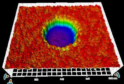
21 Copper Wire Bonding Process Reliability issues Aluminium splash on Cu bonding Splas h Depth Splas h SEM control: time consuming & partial information October 12,


22 Copper Wire Bonding Process Optical profiler Color image overlay over 3D topography Wire Bond Cavity, Depth ~ 1 µm Time to Data < 15s Sample prep = 10 mins October 12,


23 Why section is not enough? Need for 3D characterization 211% fluctuation October 12,


24 Optimisation of analysis Need for advanced functions Raw Data Remove Tilt Mask Non-Relevant Area Final Analysis 10/12/


25 Copper wire bonding Full automatic analysis Bruker Confidential Stylus and Optical Metrology Unit


26 Operator level interface One click analysis 10/12/

27 Printed Circuit Board HDI Development 10/12/


28 PCB key requirement Need longer working distance First, some sample like the IC chip below requires working distance of > 1mm so that while measuring the die at the center, the objective will not crash at the molding compound. Secondly, it is more user friendly, operator will not crash the objective on the sample easily while focusing on the sample. Z > 1 mm 10/12/


29 PCB key requirements Throughput SPEED = Image Acquisition + Data Analysis One Image Acquisition Multiple Analyses Same Speed!!! 10/12/


30 HDI PCB and Substrate Applications Via Recess / Dimple Copper Trace Roughness, depth, width on top & bottom Via Via and pad Alignment 10/12/
31 Conclusion White light interferometry profiler enables Undisturbed measurement over flexible membrane High throughput & accuracy Single characterization tool for all applications In the field of flexible electronic and PCB Contrary to other optical technic, it has intrinsic benefits of constant sub-nm vertical resolution: Safer operation PCB ready measurement 10/12/


32 Questions? Copyright Bruker Corporation. All rights reserved.


33 Thank you for joining us Join the +PE mailing list Find out how to launch your own sponsored webinar Let us know your thoughts:
Mobility and Miniaturization 3D WLI Microscopes Address Key Metrology Needs
 Mobility and Miniaturization 3D WLI Microscopes Address Key Metrology Needs Outline Introductions Brief Overview of 3D Microscopes based on WLI General technology description Benefits and general applications
NanoLens AFM and Bruker 3D Microscopes Integrated 1000X Inspection Combines for Maximum Metrology Value
 NanoLens AFM and Bruker 3D Microscopes Integrated 1000X Inspection Combines for Maximum Metrology Value Outline Introduction/Administrative Overview of Bruker 3D Optical Microscopes Software, Automation
Contour LS-K Optical Surface Profiler
 Contour LS-K Optical Surface Profiler LightSpeed Focus Variation Provides High-Speed Metrology without Compromise Innovation with Integrity Optical & Stylus Metrology Deeper Understanding More Quickly
Sample study by 3D optical profiler Contour Elite K for KTH university.
 Sample study by 3D optical profiler Contour Elite K for KTH university Samuel.lesko@bruker.com Objectives Objectives Main goals for the visit consist of evaluating 3D optical profiler: Confirm capability
Metrology Tools for Flexible Electronics and Display Substrates. Min Yang
 Metrology Tools for Flexible Electronics and Display Substrates Min Yang 1 Acknowledgement The speaker would like to sincerely thank the following collaborators for their contributions: Roger Posusta,
Advances in Disk Metrology
 Advances in Disk Metrology Robert Kertayasa Zeta Instruments March 2011 www.zeta-inst.com 1909 Concourse Drive San Jose CA 95131 PHONE (408) 577-1888 FAX (408) 577-0588 Agenda Introduction Technology Sample
EMPIR Grant Agreement 14IND07 3D Stack
 EMPIR Grant Agreement 14IND07 3D Stack Good Practice Guide: Recommendations on the strategy for measuring the dimensional properties of TSVs based on Confocal microscopy, IR interferometry and optical
3D Scratch Tester. 3D Profilometer. Scratch Tester. Fully Automated. Nano, Micro and Macro Range
 3D Scratch Tester Thin Film/ Coating Adhesion, Scratch Resistance, Hardness Wear, Roughness, Film Thickness, Sub-Nanometer Topograph Scratch Tester + 3D Profilometer Fully Automated Nano, Micro and Macro
Advantages of 3D Optical Profiling Over Other Measurement Technologies
 Horizontal milling Ra (6.35 μm, 250 uin.) Vertical milling Ra (1.6 μm, 63 uin.) Flat lapping Ra (0.2 μm, 8 uin.) Application Note #558 Correlating Advanced 3D Optical Profiling Surface Measurements to
PLASTIC FILM TEXTURE MEASUREMENT USING 3D PROFILOMETRY
 PLASTIC FILM TEXTURE MEASUREMENT USING 3D PROFILOMETRY Prepared by Jorge Ramirez 6 Morgan, Ste156, Irvine CA 92618 P: 949.461.9292 F: 949.461.9232 nanovea.com Today's standard for tomorrow's materials.
SOLAR CELL SURFACE INSPECTION USING 3D PROFILOMETRY
 SOLAR CELL SURFACE INSPECTION USING 3D PROFILOMETRY Prepared by Benjamin Mell 6 Morgan, Ste16, Irvine CA 92618 P: 949.461.9292 F: 949.461.9232 nanovea.com Today's standard for tomorrow's materials. 21
O-RING SURFACE INSPECTION USING 3D PROFILOMETRY
 O-RING SURFACE INSPECTION USING 3D PROFILOMETRY Prepared by Jorge Ramirez 6 Morgan, Ste156, Irvine CA 92618 P: 949.461.9292 F: 949.461.9232 nanovea.com Today's standard for tomorrow's materials. 2010 NANOVEA
Optical Topography Measurement of Patterned Wafers
 Optical Topography Measurement of Patterned Wafers Xavier Colonna de Lega and Peter de Groot Zygo Corporation, Laurel Brook Road, Middlefield CT 6455, USA xcolonna@zygo.com Abstract. We model the measurement
MICROSPHERE DIMENSIONS USING 3D PROFILOMETRY
 MICROSPHERE DIMENSIONS USING 3D PROFILOMETRY Prepared by Craig Leising 6 Morgan, Ste156, Irvine CA 92618 P: 949.461.9292 F: 949.461.9232 nanovea.com Today's standard for tomorrow's materials. 2010 NANOVEA
Application Note #554 VXI Universal Surface Measurements for 3D Optical Microscopes
 Surface detail of smooth AMOLED substrate Detail of LED wafer and interactive cursors Application Note #554 VXI Universal Surface Measurements for 3D Optical Microscopes MEMS inertial sensor Bruker has
Metrology for Characterization of Wafer Thickness Uniformity During 3D-IC Processing. SEMATECH Workshop on 3D Interconnect Metrology
 Metrology for Characterization of Wafer Thickness Uniformity During 3D-IC Processing SEMATECH Workshop on 3D Interconnect Metrology Chris Lee July 11, 2012 Outline Introduction Motivation For New Metrology
Embedded Power Dies for System-in-Package (SiP)
") Embedded Power Dies for System-in-Package (SiP) D. Manessis, L. Boettcher, S. Karaszkiewicz, R.Patzelt, D. Schuetze, A. Podlasky, A. Ostmann Fraunhofer Institute for Reliability and Microintegration (IZM),
Embedded Power Dies for System-in-Package (SiP) D. Manessis, L. Boettcher, S. Karaszkiewicz, R.Patzelt, D. Schuetze, A. Podlasky, A. Ostmann Fraunhofer Institute for Reliability and Microintegration (IZM),
Functional and Reactive Fluid Deposition Using Xaar Inkjet Simon Kirk Senior Product Manager Stand: A6 514
 InPrint 207 presentation - Simon Kirk - Xaar XA-0509-PU 08 Nov 207 Functional and Reactive Fluid Deposition Using Xaar Inkjet Simon Kirk Senior Product Manager Stand: A6 54 InPrint 207 presentation - Simon
AUTOFOCUS SENSORS & MICROSCOPY AUTOMATION IR LASER SCANNING CONFOCAL MICROSCOPE IRLC DEEP SEE. Now See Deeper than ever before
 AUTOFOCUS SENSORS & MICROSCOPY AUTOMATION IR LASER SCANNING CONFOCAL MICROSCOPE IRLC DEEP SEE Now See Deeper than ever before Review and inspection of non visible subsurface defects Non visible and subsurface
Sensor based adaptive laser micromachining using ultrashort pulse lasers for zero-failure manufacturing
 Sensor based adaptive laser micromachining using ultrashort pulse lasers for zero-failure manufacturing Fraunhofer Institute for Production Technology, Aachen M. Sc. Guilherme Mallmann Prof. Dr.-Ing. Robert
Bringing Patterned Media to Production with Value Added Metrology
 Bringing Patterned Media to Production with Value Added Dean Dawson, Andrew S. Lopez Diskcon /IDEMA Conference, Session 6 September 24th, 2009 Overview Introduction AFM Scan Modes New Nanotrench Pattern
ZEISS Smartproof 5 Your Integrated Widefield Confocal Microscope for Surface Analysis in Quality Assurance and Quality Control
 Product Information Version 1.0 ZEISS Smartproof 5 Your Integrated Widefield Confocal Microscope for Surface Analysis in Quality Assurance and Quality Control Dedicated Design. Guided Workflow. Trusted
Phenom TM Pro Suite. The ultimate application software solution. Specification Sheet
 Phenom TM Pro Suite The ultimate application software solution The Phenom TM Pro Suite is developed to enable Phenom users to extract maximum information from images made with the Phenom G2 pro desktop
FOCALSPEC 3D LINE CONFOCAL SCANNER UULA DID THEY TELL YOU THAT NO-ONE CAN MEASURE IT? WE CAN.
 FOCALSPEC 3D LINE CONFOCAL SCANNER UULA DID THEY TELL YOU THAT NO-ONE CAN MEASURE IT? WE CAN. FocalSpec 3D Line Confocal Scanner UULA UULA is an automated optical 3D imaging and metrology system for sub-micron
Comparison & highlight on the last 3D TSV technologies trends Romain Fraux
 Comparison & highlight on the last 3D TSV technologies trends Romain Fraux Advanced Packaging & MEMS Project Manager European 3D Summit 18 20 January, 2016 Outline About System Plus Consulting 2015 3D
NON-CONTACT 3D SURFACE METROLOGY
 LOGO TITLE NON-CONTACT 3D SURFACE METROLOGY COMPANY PROFILE SLOGAN BECAUSE ACCURACY MATTERS LASERSCRIBING MEASUREMENT INTRODUCTION One of the last steps in the production of electronic components is the
MicraGEM-Si A flexible process platform for complex MEMS devices
 MicraGEM-Si A flexible process platform for complex MEMS devices By Dean Spicer, Jared Crawford, Collin Twanow, and Nick Wakefield Introduction MicraGEM-Si is a process platform for MEMS prototyping and
New Approach in Non- Contact 3D Free Form Scanning
 New Approach in Non- Contact 3D Free Form Scanning Contents Abstract Industry Trends The solution A smart laser scanning system Implementation of the laser scanning probe in parts inspection Conclusion
Veeco Expands Solar Equipment Product Line Acquisition of Mill Lane Engineering. May 22, 2008
 Veeco Expands Solar Equipment Product Line Acquisition of Mill Lane Engineering May 22, 2008 Veeco Expands Thin Film Solar Equipment Product Line Completed purchase of Mill Lane Engineering Privately held
Scanning Acoustic Microscopy For Metrology of 3D Interconnect Bonded Wafers
 Scanning Acoustic Microscopy For Metrology of 3D Interconnect Bonded Wafers Jim McKeon, Ph.D. - Sonix, Director of Technology Sriram Gopalan, Ph.D. - Sonix, Technology Engineer 8700 Morrissette Drive 8700
DENTAL WEAR SURFACE USING 3D PROFILOMETRY
 DENTAL WEAR SURFACE USING 3D PROFILOMETRY Prepared by Ali Mansouri 6 Morgan, Ste156, Irvine CA 92618 P: 949.461.9292 F: 949.461.9232 nanovea.com Today's standard for tomorrow's materials. 2016 NANOVEA
Opto-digital microscopy The future of industrial quality control
 Opto-digital microscopy The future of industrial quality control Abstract: Industrial quality assessment tasks Function often relates to form, and this holds particular truth within the world of manufacturing.
Polymer Micro-Optics for Today s Compact Photonic Devices
 Polymer Micro-Optics for Today s Compact Photonic Devices Lynn Dobosz - North America Sales & Business Development for the Opto-Electronic Systems business unit of the Optical Systems division of Jenoptik
STEP HEIGHT MEASUREMENT OF PRINTED ELECTRODES USING 3D PROFILOMETRY
 STEP HEIGHT MEASUREMENT OF PRINTED ELECTRODES USING D PROFILOMETRY Prepared by Andrea Herrmann Morgan, Ste, Irvine CA 98 P: 99..99 F: 99..9 nanovea.com Today's standard for tomorrow's materials. NANOVEA
Optical 3D measurements capture the entire surface with nanometer precision
 Optical 3D measurements capture the entire surface with nanometer precision Traceability of any structure to the gold standard of stylus profilometers as used by Germany s National Metrology Institute
MEMS SENSOR FOR MEMS METROLOGY
 MEMS SENSOR FOR MEMS METROLOGY IAB Presentation Byungki Kim, H Ali Razavi, F. Levent Degertekin, Thomas R. Kurfess 9/24/24 OUTLINE INTRODUCTION Motivation Contact/Noncontact measurement Optical interferometer
UULA FOCALSPEC 3D LINE CONFOCAL SCANNER DID THEY TELL YOU THAT NO-ONE CAN MEASURE IT? WE CAN.
 FocalSpec builds optical sensors to measure and inspect the quality of the advanced materials and devices in use today and currently in development for the future. Our sensors combine 3D topography, 3D
ECP Embedded Component Packaging Technology
 ECP Embedded Component Packaging Technology A.Kriechbaum, H.Stahr, M.Biribauer, N.Haslebner, M.Morianz, M.Beesley AT&S Austria Technologie und Systemtechnik AG Abstract The packaging market has undergone
WARPAGE MEASUREMENT OF PCB USING 3D PROFILOMETRY
 WARPAGE MEASUREMENT OF PCB USING 3D PROFILOMETRY Prepared by Craig Leising 6 Morgan, Ste156, Irvine CA 92618 P: 949.461.9292 F: 949.461.9232 nanovea.com Today's standard for tomorrow's materials. 2010
9 rue Alfred Kastler - BP Nantes Cedex 3 - France Phone : +33 (0) website :
 website :") 9 rue Alfred Kastler - BP 10748-44307 Nantes Cedex 3 - France Phone : +33 (0) 240 180 916 - email : info@systemplus.fr - website : www.systemplus.fr August 2011 - Version 1 Written by: Sylvain HALLEREAU
9 rue Alfred Kastler - BP 10748-44307 Nantes Cedex 3 - France Phone : +33 (0) 240 180 916 - email : info@systemplus.fr - website : www.systemplus.fr August 2011 - Version 1 Written by: Sylvain HALLEREAU
9 rue Alfred Kastler - BP Nantes Cedex 3 - France Phone : +33 (0) website :
 website :") 9 rue Alfred Kastler - BP 10748-44307 Nantes Cedex 3 - France Phone : +33 (0) 240 180 916 - email : info@systemplus.fr - website : www.systemplus.fr May 2011 - Version 2 Written by: Sylvain HALLEREAU DISCLAIMER
9 rue Alfred Kastler - BP 10748-44307 Nantes Cedex 3 - France Phone : +33 (0) 240 180 916 - email : info@systemplus.fr - website : www.systemplus.fr May 2011 - Version 2 Written by: Sylvain HALLEREAU DISCLAIMER
Bringing 3D Integration to Packaging Mainstream
 Bringing 3D Integration to Packaging Mainstream Enabling a Microelectronic World MEPTEC Nov 2012 Choon Lee Technology HQ, Amkor Highlighted TSV in Packaging TSMC reveals plan for 3DIC design based on silicon
AVT-1000 Advanced Vibrometry Tester. Cutting Edge Optical Surface Analyzer Technology for Nano-defect and Topography Measurements
 AVT-1000 Advanced Vibrometry Tester Cutting Edge Optical Surface Analyzer Technology for Nano-defect and Topography Measurements Using the Best Technology... Why use Advanced Vibrometry? Repeatability:
TLS-Dicing for concentrator dies - a fast and clean technology. Hans-Ulrich Zühlke
 TLS-Dicing for concentrator dies - a fast and clean technology Hans-Ulrich Zühlke TLS-Dicing with JENOPTIK-VOTAN Semi Contents Overview Jenoptik Principle of TLS-Technology TLS-Dicing the benefits at a
Step Height Comparison by Non Contact Optical Profiler, AFM and Stylus Methods
 AdMet 2012 Paper No. NM 002 Step Height Comparison by Non Contact Optical Profiler, AFM and Stylus Methods Shweta Dua, Rina Sharma, Deepak Sharma and VN Ojha National Physical Laboratory Council of Scientifi
POWDER COATING FINISH MEASUREMENT USING 3D PROFILOMETRY
 POWDER COATING FINISH MEASUREMENT USING 3D PROFILOMETRY Prepared by Craig Leising 6 Morgan, Ste156, Irvine CA 92618 P: 949.461.9292 F: 949.461.9232 nanovea.com Today's standard for tomorrow's materials.
3D-Analysis of Microstructures with Confocal Laser Scanning Microscopy
 3D-Analysis of Microstructures with Confocal Laser Scanning Microscopy Eckart Uhlmann, Dirk Oberschmidt Institute for Machine Tools and Factory Management (IWF), Technical University Berlin Gerald Kunath-Fandrei
MACHINING SURFACE FINISH QUALITY USING 3D PROFILOMETRY
 MACHINING SURFACE FINISH QUALITY USING 3D PROFILOMETRY Prepared by Duanjie Li, PhD Morgan, Ste1, Irvine CA 91 P: 99.1.99 F: 99.1.93 nanovea.com Today's standard for tomorrow's materials. 1 NANOVEA INTRODUCTION
Compact non-contact 3D surface profiler
 Compact non-contact 3D surface profiler Compact. Flexible. Powerful. S lynx is a new non-contact 3D surface profiler designed for use in industry and research. It has been designed as a compact and versatile
Precise flatness measurement
 NEW Simple Roughness and flatness in one measurement Reliable Measurement of step heights High Precision Measurements down to the nanometer range Safe Accuracy in deep layers Efficient Semi-automatic series
Memjet ML Printhead from the RapidX1 Color Label Printer
 ML210700 Printhead from the RapidX1 Color Label Printer MEMS Process Review 3685 Richmond Road, Suite 500, Ottawa, ON K2H 5B7 Canada Tel: 613-829-0414 www.chipworks.com MEMS Process Review Some of the
ULTRA-THIN DOUBLE LAYER METROLOGY WITH HIGH LATERAL RESOLUTION. Semicon West 2018, Bernd Srocka
 ULTRA-THIN DOUBLE LAYER METROLOGY WITH HIGH LATERAL RESOLUTION Semicon West 2018, Bernd Srocka Mission Unity-SC provides a wide range of Solutions in Metrology& inspection to the Semiconductor Industry,
T-Solar Overview. * Patent-pending
 T-Solar T-Solar Overview The T-Solar system combines our best photovoltaic measurement technology into a system designed specifically for measuring textured samples. Based on the established M-2000 rotating
Fast Z-stacking 3D Microscopy Extended Depth of Field Autofocus Z Depth Measurement 3D Surface Analysis
 MICROSCOPE 3D ADD-ON FAST PRECISE AFFORDABLE 3D ADD-ON FOR MICROSCOPY Fast Z-stacking 3D Microscopy Extended Depth of Field Autofocus Z Depth Measurement 3D Surface Analysis Compatible With Transmitted
SURFACE TEXTURE EFFECT ON LUSTER OF ANODIZED ALUMINUM USING 3D PROFILOMETRY
 SURFACE TEXTURE EFFECT ON LUSTER OF ANODIZED ALUMINUM USING 3D PROFILOMETRY Prepared by Duanjie Li, PhD 6 Morgan, Ste156, Irvine CA 92618 P: 949.461.9292 F: 949.461.9232 nanovea.com Today's standard for
3D Surface Analysis Form & Roughness Measurement Automatic Depth Composition Z Depth Measurement
 MICROSCOPE 3D ADD ON FAST PRECISE AFFORDABLE 3D ADD ON FOR MICROSCOPES 3D Surface Analysis Form & Roughness Measurement Automatic Depth Composition Z Depth Measurement Compatible With Compound Microscopes
Optical 3D surface measurement technology for research and industry
 Optical 3D surface measurement technology for research and industry Company profile and product overview Technology leader in optical 3D metrology for functional surfaces NanoFocus AG is a developer, manufacturer,
3D OPTICAL PROFILER MODEL 7503
 3D Optical Profiler MODEL 7503 Features: 3D OPTICAL PROFILER MODEL 7503 Chroma 7503 is a sub-nano 3D Optical Profiler developed using the technology of white light interference to measure and analyze the
Compact 3D optical surface profiler
 Compact 3D optical surface profiler Compact. Flexible. Powerful. S lynx is a new non-contact 3D surface profiler designed for use in industry and research. It has been designed as a compact and versatile
CHARACTERIZATION OF FISH SCALE USING 3D PROFILOMETRY
 CHARACTERIZATION OF FISH SCALE USING 3D PROFILOMETRY 2 4 6 8 1 mm 1 2 3 4 5 6 7 8 mm Prepared by Andrea Novitsky 6 Morgan, Ste156, Irvine CA 92618 P: 949.461.9292 F: 949.461.9232 nanovea.com Today's standard
Surface Texture Measurement Fundamentals
 Surface Texture Measurement Fundamentals Dave MacKenzie Slide 1 Presentation Scope Examples of Why We Measure Surface Texture Stylus Based Instruments Stylus Tracing Methods Filters and Cutoff Basic Parameters
TrueSurface Microscopy. Confocal Microscopy Along with Large Area Optical Profiling.
 TrueSurface Microscopy Confocal Microscopy Along with Large Area Optical Profiling www.witec.de alpha500 with sensor for profilometry Features & Benefits Extension for the WITec alpha500 series that combines
3D Surface Metrology on PV Solar Wafers
 3D Surface Metrology on PV Solar Wafers Karl- Heinz Strass cybertechnologies USA 962 Terra Bella Ave San Jose CA 95125 P: 408-689-8144 www.cybertechnologies.com Introduction Solar photovoltaics is the
TISSUE SURFACE TOPOGRAPHY USING 3D PRFILOMETRY
 TISSUE SURFACE TOPOGRAPHY USING 3D PRFILOMETRY Prepared by Craig Leising 6 Morgan, Ste156, Irvine CA 92618 P: 949.461.9292 F: 949.461.9232 nanovea.com Today's standard for tomorrow's materials. 2011 NANOVEA
SURFACE BOUNDARY MEASUREMENT USING 3D PROFILOMETRY
 SURFACE BOUNDARY MEASUREMENT USING 3D PROFILOMETRY Prepared by Craig Leising 6 Morgan, Ste156, Irvine CA 92618 P: 949.461.9292 F: 949.461.9232 nanovea.com Today's standard for tomorrow's materials. 2013
3D SYSTEM INTEGRATION TECHNOLOGY CHOICES AND CHALLENGE ERIC BEYNE, ANTONIO LA MANNA
 3D SYSTEM INTEGRATION TECHNOLOGY CHOICES AND CHALLENGE ERIC BEYNE, ANTONIO LA MANNA OUTLINE 3D Application Drivers and Roadmap 3D Stacked-IC Technology 3D System-on-Chip: Fine grain partitioning Conclusion
Package (1C) Young Won Lim 3/13/13
 Young Won Lim 3/13/13") Copyright (c) 2011-2013 Young W. Lim. Permission is granted to copy, distribute and/or modify this document under the terms of the GNU Free Documentation License, Version 1.2 or any later version published
Copyright (c) 2011-2013 Young W. Lim. Permission is granted to copy, distribute and/or modify this document under the terms of the GNU Free Documentation License, Version 1.2 or any later version published
IDEMA, March Hari Hegde CTO, Data Storage Process Equipment Veeco Instruments Inc.
 Era of HDD s for Consumer Electronics: Slider Technology Process Solutions IDEMA, March 2005 Hari Hegde CTO, Data Storage Process Equipment Veeco Instruments Inc. Overview Disk Drive Industry Rejuvenation
STEEL SURFACE CHARACTERIZATION USING 3D PROFILOMETRY
 STEEL SURFACE CHARACTERIZATION USING 3D PROFILOMETRY Prepared by Andrea Novitsky 6 Morgan, Ste156, Irvine CA 92618 P: 949.461.9292 F: 949.461.9232 nanovea.com Today's standard for tomorrow's materials.
Portal del coneixement obert de la UPC
 UPCommons Portal del coneixement obert de la UPC http://upcommons.upc.edu/e-prints A. Matilla and J. Mariné and J. Pérez and C. Cadevall and R. Artigas, "Three-dimensional measurements with a novel technique
AT&S Company. Presentation. 3D Component Packaging. in Organic Substrate. Embedded Component. Mark Beesley IPC Apex 2012, San Diego.
 3D Component Packaging AT&S Company in Organic Substrate Presentation Embedded Component Mark Beesley IPC Apex 2012, San Diego www.ats.net Austria Technologie & Systemtechnik Aktiengesellschaft Fabriksgasse13
Leica DCM 3D. Dual Core 3D Profiler combines Confocal Imaging and Interferometry. Living up to Life
 Leica DCM 3D Dual Core 3D Profiler combines Confocal Imaging and Interferometry Living up to Life Automated Digital 3D Topography Measurement in High Definition In recent years, the competing technologies
FST s status on EUV Pellicle & Inspection System Development
 FST s status on EUV Pellicle & Inspection System Development OCT.04, 2015 EUV Pellicle TWG @ Imec, nl. Donwon Park FST (Korea) http://www.fstc.co.kr FST Business Segments Division Pellicle TCU (Temperature
Length, Singapore, NMC, A*STAR (National Metrology Centre, Agency for Science, Technology and Research)
") Calibration or m 633 633 nm 0.5 MHz 2 95% No LS/L/001 633 633 nm 0.016 fm 2 95% No LS/L/003 474 474 THz 12 khz 2 95% No LS/L/003 543 633 nm 0.0016 fm 2 95% No LS/L/003 553 474 THz 1.2 khz 2 95% No LS/L/003
Calibration or m 633 633 nm 0.5 MHz 2 95% No LS/L/001 633 633 nm 0.016 fm 2 95% No LS/L/003 474 474 THz 12 khz 2 95% No LS/L/003 543 633 nm 0.0016 fm 2 95% No LS/L/003 553 474 THz 1.2 khz 2 95% No LS/L/003
Test and Measurement Challenges for 3D IC Development. R. Robertazzi IBM Research
 Test and Measurement Challenges for 3D IC Development R. Robertazzi IBM Research PFA Bill Price. Pete Sorce. John Ott. David Abraham. Pavan Samudrala Digital Test Kevin Stawaisz. TEL P12 Prober Glen Lansman,
Jr25 OPTICAL OPTIONS. 20 x 30 x 17 cm
 PROFILOMETERS Nanovea Profilometers are designed with leading edge Chromatic Confocal optical technology (axial chromatism) both ISO and ASTM compliant. The technique measures a physical wavelength directly
Improvement of the correlative AFM and ToF-SIMS approach using an empirical sputter model for 3D chemical characterization
 Improvement of the correlative AFM and ToF-SIMS approach using an empirical sputter model for 3D chemical characterization T. Terlier 1, J. Lee 1, K. Lee 2, and Y. Lee 1 * 1 Advanced Analysis Center, Korea
Package (1C) Young Won Lim 3/20/13
 Young Won Lim 3/20/13") Copyright (c) 2011-2013 Young W. Lim. Permission is granted to copy, distribute and/or modify this document under the terms of the GNU Free Documentation License, Version 1.2 or any later version published
Copyright (c) 2011-2013 Young W. Lim. Permission is granted to copy, distribute and/or modify this document under the terms of the GNU Free Documentation License, Version 1.2 or any later version published
ZEISS Launches New High-resolution 3D X-ray Imaging Solutions for Advanced Semiconductor Packaging Failure Analysis
 Press Release ZEISS Launches New High-resolution 3D X-ray Imaging Solutions for Advanced Semiconductor Packaging Failure Analysis New submicron and nanoscale XRM systems and new microct system provide
PRODUCTION OF ULTRA-FLAT SEMICONDUCTOR WAFER SUBSTRATES USING ADVANCED OPTICAL LENS POLISHING TECHNOLOGY
 PRODUCTION OF ULTRA-FLAT SEMICONDUCTOR WAFER SUBSTRATES USING ADVANCED OPTICAL LENS POLISHING TECHNOLOGY / Slide 1 IQBAL (IZZY) BANSAL ASML HOLDING (NV) iqbalbansal@asml.com JANUARY 10, 2009
ABSTRACT 1. INTRODUCTION
 Copyright 2016 Society of Photo-Optical Instrumentation Engineers. One print or electronic copy may be made for personal use only. Systematic reproduction and distribution, duplication of any material
CARBON FIBER SURFACE MEASUREMENT USING 3D PROFILOMETRY
 CARBON FIBER SURFACE MEASUREMENT USING 3D PROFILOMETRY Prepared by Craig Leising 6 Morgan, Ste156, Irvine CA 92618 P: 949.461.9292 F: 949.461.9232 nanovea.com Today's standard for tomorrow's materials.
SPECTRUM. The world s first fully automated Raman AFM. AFM - confocal Raman - SNOM - TERS AFM KPFM. Raman. AFM-Raman characterization of PS-PVAC
 Raman KPFM AFM AFM-Raman characterization of PS-PVAC polymer blend film SPECTRUM The world s first fully automated Raman AFM AFM - confocal Raman - SNOM - TERS The first fully integrated & automated AFM
SURFACE TEXTURE CONSISTENCY USING 3D PROFILOMETRY
 SURFACE TEXTURE CONSISTENCY USING 3D PROFILOMETRY Prepared by Craig Leising 6 Morgan, Ste156, Irvine CA 92618 P: 949.461.9292 F: 949.461.9232 nanovea.com Today's standard for tomorrow's materials. 2013
SURFACE FINISH INSPECTION OF WOOD USING 3D PROFILOMETRY
 SURFACE FINISH INSPECTION OF WOOD USING 3D PROFILOMETRY Prepared by Duanjie Li & Craig Leising 6 Morgan, Ste156, Irvine CA 92618 P: 949.461.9292 F: 949.461.9232 nanovea.com Today's standard for tomorrow's
Micron Level Placement Accuracy for Wafer Scale Packaging of P-Side Down Lasers in Optoelectronic Products
 Micron Level Placement Accuracy for Wafer Scale Packaging of P-Side Down Lasers in Optoelectronic Products Daniel D. Evans, Jr. and Zeger Bok Palomar Technologies, Inc. 2728 Loker Avenue West Carlsbad,
High Value Manufacturing for Low Cost Electronics
 High Value Manufacturing for Low Cost Electronics 10th Anniversary High Value Manufacturing Conference 2012 14 November 2012 Cambridge www.cir-strategy.com/events/ PragmatIC Printing enables printed logic
Cantilever Based Ultra Fine Pitch Probing
 Cantilever Based Ultra Fine Pitch Probing Christian Leth Petersen Peter Folmer Nielsen Dirch Petersen SouthWest Test Workshop San Diego, June 2004 1 About CAPRES Danish MEMS probe & interfacing venture
A RADIAL WHITE LIGHT INTERFEROMETER FOR MEASUREMENT OF CYLINDRICAL GEOMETRIES
 A RADIAL WHITE LIGHT INTERFEROMETER FOR MEASUREMENT OF CYLINDRICAL GEOMETRIES Andre R. Sousa 1 ; Armando Albertazzi 2 ; Alex Dal Pont 3 CEFET/SC Federal Center for Technological Education of Sta. Catarina
University of Minnesota Nano Fabrication Center Standard Operating Procedure
 Equipment Name: University of Minnesota Nano Fabrication Center Coral Name: hs-scope Revision Number: 1.5 Model: HS200A Revisionist: M. Fisher Location: Bay 1 Date: 9/12/2013 1 Description The Hyphenated
Inspection System for High-Yield Production of VLSI Wafers
 Inspection System for High-Yield Production of VLSI Wafers Toshimitsu Hamada 1), Jun Nakazato 2), Kenji Watanabe 3), Fumio Mizuno 4), Shizuo Isogai 5) 1) Nasu University, Faculty of Urban Economics 2)
H.-J. Jordan (NanoFocus Messtechnik GmbH), R. Brodmann (Brodmann Marketing & Vertrieb)
, R. Brodmann (Brodmann Marketing & Vertrieb)") Highly accurate surface measurement by means of white light confocal microscopy Hochgenaue Oberflächenmessung mit Hilfe von konfokalen Weißlichttechniken H.-J. Jordan (NanoFocus Messtechnik GmbH), R. Brodmann
Highly accurate surface measurement by means of white light confocal microscopy Hochgenaue Oberflächenmessung mit Hilfe von konfokalen Weißlichttechniken H.-J. Jordan (NanoFocus Messtechnik GmbH), R. Brodmann
Monolithic 3D Integration using Standard Fab & Standard Transistors. Zvi Or-Bach CEO MonolithIC 3D Inc.
 Monolithic 3D Integration using Standard Fab & Standard Transistors Zvi Or-Bach CEO MonolithIC 3D Inc. 3D Integration Through Silicon Via ( TSV ), Monolithic Increase integration Reduce interconnect total
Packaging for parallel optical interconnects with on-chip optical access
 Packaging for parallel optical interconnects with on-chip optical access I. INTRODUCTION Parallel optical interconnects requires the integration of lasers and detectors directly on the CMOS chip. In the
Lockheed Martin Nanosystems
 Lockheed Martin Nanosystems National Nanotechnology Initiative at Ten: Nanotechnology Innovation Summit December 2010 Dr. Brent M. Segal Director & Chief Technologist, LM Nanosystems brent.m.segal@lmco.com
Embedded UTCP interposers for miniature smart sensors
 Embedded UTCP interposers for miniature smart sensors T. Sterken 1,2, M. Op de Beeck 2, Tom Torfs 2, F. Vermeiren 1,2, C. Van Hoof 2, J. Vanfleteren 1,2 1 CMST (affiliated with Ugent and IMEC), Technologiepark
MEMS - Exhibitor Presentations Manufacturing Technology and Quality Multi Sensor Metrology for Control of MEMS Production
 MEMS - Exhibitor Presentations Manufacturing Technology and Quality Multi Sensor Metrology for Control of MEMS Production Dr. Bastian Marheineke FRT, Fries Research & Technology GmbH marheineke@frt-gmbh.com
The Dektak XT is a 2D contact profilometer used for step height, pitch and surface roughness
 Dektak XT 2D Profilometer Operation Manual The Dektak XT is a 2D contact profilometer used for step height, pitch and surface roughness measurements. Vision 64 application software controls the system
Company Backgrounder. Overview
 Company Backgrounder Overview FUJIFILM Dimatix, Inc., a wholly owned subsidiary of FUJIFILM Corporation and the world s leading supplier of piezoelectric drop-on-demand inkjet products used for industrial
Chemical Characterization of Diverse Pharmaceutical Samples by Confocal Raman Microscopy
 Whitepaper Chemical Characterization of Diverse Pharmaceutical Samples by Confocal Raman Microscopy WITec GmbH, Lise-Meitner-Str. 6, 89081 Ulm, Germany, www.witec.de Introduction The development and production