HOMEWORK 9 CMPEN 411 Due: 4/12/ :30pm
|
|
|
- Samantha Collins
- 6 years ago
- Views:
Transcription

1 HOMEWORK 9 CMPEN 411 Due: 4/12/ :30pm Learning Objective Complete the full 8 bit RISC microprocessor chip design by placing the processor core design into the 40 pin 'tiny' chip pad frame. Do verify the functioning and timing from the 'pad-to-pad' simulation. Instruction This semester, we are building a simple microprocessor shown below. It is an 8-bit RISC processor, its full description and specification is posted at: Now the microprocessor core design needs to be placed into the chip pad frame to complete the chip. Sample pad frame 'p3tinyfr1' for the class chip fabrication, 40 pins total, 1000um X 1000um inside area
2 1. Homework 9 preparation: Create a directory 'hw9yourlastname' under c411 directory (assuming you have c411 directory in your home for this class). Change the current directory to hw9yourlastname. Set up the directory for a new Cadence Virtuoso library. Then start the hw9 design project. For example, my hw9 directory will be 'hw9choi' and I will be running the following unix commands right after I login to my account: % cd c411 % mkdir hw9choi % cd hw9choi % runcds % virtuoso & You can follow the same except that you need to use your last name after 'hw9'. 2. Once the Virtuoso is running, create the new library named 'hw9yourlastname' first. Attach the NCSU_TechLib_ami06 technology to your 'hw9yourlastname' library. Then exit the Virtuoso to add the pad frame library path and your hw8 library path to your hw9 project. One can manually add some library paths to hw9 project and copy all the necessary cells from those library to the new hw9 library. After copying all the cells, one MUST delete the other library paths, leaving only the 'hw9yourlastname' library, containing all the cells for the complete chip. 3. Collect all the components (cells) in the hw9yourlastname library, it will be 'tar' and 'zipped', and turn-in to the instructor for grading. Please use 'Copy Wizard...' from the virtuoso library manager to copy your previous homework cells and the instructor's pad frame cells to the hw9yourlastname library. This way, you can collect all the files into the hw9yourlastname directory and it will allow the grading. Otherwise, your hw9 project folder results in missing files which will cause the design verification for grade to fail. You will lose points if your turned-in hw9 design files cannot be verified by grader due to missing files or cells. 4. To manually add the library path, I will be running the following unix editing command for cmpen 411 class: % xe cds.lib The file cds.lib exists in your hw9yourlastname directory once you created the library hw9yourlastname with Virtuoso. My file contains the following two lines: INCLUDE /home/noncse/kyusunt/cds.lib DEFINE hw9choi /home/noncse/kyusunt/cmpen411/hw9choi/hw9choi Similarly, your cds.lib file will contain your account path and hw9yourlastname in place of mine above. Then I will add the following two lines: DEFINE hw8choi /home/noncse/kyusunt/cmpen411/hw8choi/hw8choi DEFINE p500tiny /home/faculty/kyusun/c411/cd6/ncs/c50/padkc/p500tiny The first line is to add my hw8 library to my hw9 project. You must type your directory path and hw8yourlastname in place of my information. The second line is to add the p500tiny pad library to your hw9 project, you must type it exactly as it is shown. So the overall cds.lib file will contain the following four lines in my case: INCLUDE /home/noncse/kyusunt/cds.lib DEFINE hw9choi /home/noncse/kyusunt/cmpen411/hw9choi/hw9choi DEFINE hw8choi /home/noncse/kyusunt/cmpen411/hw8choi/hw8choi DEFINE p500tiny /home/faculty/kyusun/c411/cd6/ncs/c50/padkc/p500tiny Now be sure to save the file and Quit the cds.lib file editing.

3 5. To copy the cells from your hw8 and the p500tiny library, run Virtuoso. Once the Virtuoso is running, the library manager will show the two libraries: hw8yourlastname and p500tiny in addition to your hw9yourlastname library. First select the hw8yourlastname library in your Library Manager window. Then select the 'Copy Wizard...' option under the 'Edit' pull-down menu in the library manager. The 'Copy Wizard' window will pop. Set the 'Destination Library' to your hw9yourlastname. Then select the cells from your hw8 library to be copied to your hw9 library. You will need to copy Layout, Schematic, and Symbol files of each cell. Click 'OK' to copy them. Then select the p500tiny library in your Library Manager window. Again, select the 'Copy Wizard...' option under the 'Edit' pull-down menu in the library manager. The 'Copy Wizard' window will pop. Set the 'Destination Library' to your hw9yourlastname. Then select the cells (all the cells) from the p500tiny library to be copied to your hw9 library. Again, you will need to copy Layout, Schematic, and Symbol files of each cell. Click 'OK' to copy them. Now quit (Exit) Virtuoso. 6. Once all the cells needed are copied to your hw9 library, you MUST delete the hw8 and p500tiny library paths from the cds.lib file. To do that, again edit cds.lib file and delete the last two lines. This will leave only the hw9 library in your Library Manager the next time you start the Virtuoso. In this way, your hw9 library will contain all the needed cells once you finished the project. 7. Use hierarchical design method to manage design complexity. That is, design simple cells and design top cell which combines simple cells. The Cadence tool Virtuoso assumes all design is done this way, uses cellview to manage cells. Use meaningful names for the cells; for example, use 8bitMicroprocessor rather than hw8 for the microprocessor. For your hw9 project, you MUST name 'aaamicro8top' as the top cell - the complete chip. 8. Now complete the full 8 bit RISC microprocessor chip design by placing the processor core design into the 40 pin 'tiny' chip pad frame. Do verify the functioning and timing from the 'pad-to-pad' simulation. 9. As in any chip design, the design goal is to layout the circuit in a small area, and achieve very fast signal communication. You may want to re-shape and update your design so that it will fit the 40 pin pad frame. Do assign each pin pad for the input, output, program data, vdd, gnd, clock, reset, etc. There are only 40 pins, any left-over pins can be used for testing signals. 10. The pads in the frame can be re-arranged. Any pad can be replaced with another pad. There are input signal pad, output signal pad, in/out bidirectional signal pad, vdd pad, gnd pad, etc. pin The final chip pin signal assignment must be made in the following way:
 a 21 bit shift register to program the processor chip's SRAM in serial fashion, and (2) a on-chip clock circuit to generate internal clock signal.")
4 12. Final chip die will be placed in the 40 pin Dual In-line Package (DIP), the bonding wire placement from the chip pads to the package pin leads is shown below (top view): 13. Add two new circuits to the chip: (1) a 21 bit shift register to program the processor chip's SRAM in serial fashion, and (2) a on-chip clock circuit to generate internal clock signal. The schematic diagrams are shown in Appendix A below. 14. Be sure to connect all of the power vdd! and gnd! lines with thicker metal layers (m1 or m2 or m3). Also use as many contacts as possible for the power line connections. 15. Be sure to put the signal labels on the bonding pad with m3 layer. Also be sure to include at least one vdd pad and one gnd pad, and label them. Make only one vdd! label and one gnd! label. 16. The design must be free from the DRC errors and pass the LVS checking. 17. Extract the circuit from the layout including the parasitic capacitances. Then hspice simulate the extracted circuit netlist. Any of the timing measurements required for the questions below must use the simulation of the extracted
5 circuit from the layout including the parasitic capacitances. Place 1pF load capacitor on the output pads, in.hsp file for the pad to pad simulation. 18. To verify the functioning, design the Hspice simulation files:.hsp,.s, and.sp files. Your simulation output must show all signals. Design your.hsp file to show the following eight instruction executions in sequence. However, the program execution must be proceeded by the program storing in the program memory through the pads. So, the simulation must include program storing and then program execution. Explain your simulation: writing and execution sequence with the signals. The timing must include pads and load capacitors on the output pads. MV 0,0 MV #9,5 MV #8,7 MV 7,0 ADD 5,0 SUB 5,7 BC 6 IN 3 OUT You can always add more labels on the layout to see the microprocessor internal signals on the simulation output. This will help debugging the processor, visualizing the signal propagation, and analyzing the circuits. 20. For your microprocessor simulation, explain the instruction execution time. How do you measure the instruction execution time from the simulation result? Please explain. What is the worst case instruction execution time of your microprocessor? Please explain the worst case instruction execution time. 21. How fast can you repeat the clock signal CK while the program properly executing? 22. From the instruction execution simulation, list the delay times of each sub operations, which will be added to make up the one instruction execution cycle. Do for all 7 instructions. Which instruction is the fastest? Which instruction is the slowest? Why? Explain. 23. Which component is the slowest? Why does it take so long? How can we make it faster? Design the.hsp file to demonstrate the worst case instruction execution of the microprocessor while maintaining the correct output result. What limits the maximum speed of operation? Show the simulation plot to substantiate your answer. 24. How many transistors are used in your microprocessor chip design (including the pads)? 25. Did you use static, dynamic, or pass transistor logic? 26. Are there any errors in schematic? 27. Is there an error in layout? Does your layout pass the DRC checking without errors (including the pads)? 28. Is there a miss match on the schematic versus layout? Does your design pass the LVS checking without errors (including the pads)? 29. Extract the circuit from the layout including the parasitic capacitances. Then hspice simulate the extracted circuit netlist. Be sure that your signal label is placed at the pad so that the simulation is 'pad-to-pad' signal simulation. What is the worst case output signal rise time, fall time, and delay time? The worst case delay time is from which input to which output? Explain the signal path for the worst case delay time (this is called critical signal path)? Worst case delay time: T = nsec.
6 30. What is the total layout height and width? What is the total layout area measured in um**2? Area: A = um**2 (including the pads). 31. What is the AT**2 measure of your design? AT**2 = um**2 nsec**2 (including the pads). 32. Create a hw9 report file hw9yourlastname.doc and include captured image of layout and the simulation results. Add your explanations and comments. On the Linux machines in room 218 IST, one can use 'openoffice.org' program for the document creating and editing, and use 'gimp' program for the image capture and processing from the screen. 33. The hw9 report file must also include the answers to the questions. 34. The hw9 report file can be in.doc or.pdf, must include a cover page for student information such as 'CMPEN 411, Homework 9, your name, etc. Please use the sample Homework 9 report format, the sample hw9 report file is posted: Sample hw9 Report 35. Create a tarred zip file of your hw9yourlastname directory in c411 directory. It will contain the schematics, symbols, layouts,.hsp,.sp files, and.doc report file. In your c411 directory, use the following unix commands % tar -czvf hw9yourlastname.tgz hw9yourlatname to create a tarred zip file of hw9yourlastname library. For example, % tar -czvf hw9choi.tgz hw9choi will archive the directory hw9choi and create a zipped file hw9choi.tgz in my c411 project directory. For the grading, the command tar xzvf hw9choi.tgz will be used to restore project. Please delete.tr0 files before zipping, for their sizes are usually large. 36. Turn-in your project zip file through Penn State ANGEL. Deposit your zip file into the Homework 9 DropBox under CLASS tab in CMPEN 411 Course. 37. Make sure that you include all the files necessary into your project folder, in order to verify for grading. Turn-in your project before 11:30pm on the due date. Apendix A (1) The 21 bit shift register diagram: The 21 bit shift register signal connection diagram. Chip pins: SI (Data Shift-In), SO (Data Shift-Out, same as widat<0>), and ck-sh (Data Shifting Clock) are associated with this circuit.


7 The 21 bit shift register schematic diagram. Zoom-in view of the 21 bit shift register schematic diagram, left part. Zoom-in view of the 21 bit shift register schematic diagram, middle part. Zoom-in view of the 21 bit shift register schematic diagram, right part. Please note the output signal names.
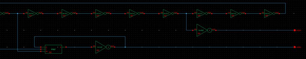
, ckb-out (Clockb-out), osfstart (Oscillator Frequency Start), osfout (Oscillator Frequency Out), osfs<1>, and")

8 (2) The on-chip clock circuit: The on-chip clock circuit block diagram. Chip pins: ck-in (Clock-In), ckb-out (Clockb-out), osfstart (Oscillator Frequency Start), osfout (Oscillator Frequency Out), osfs<1>, and osfs<0> (Oscillator Frequency Select) are associated with this circuit. The 31 state ring oscillator schematic diagram. Zoom-in view of the 31 state ring oscillator schematic diagram, left part. Zoom-in view of the 31 state ring oscillator schematic diagram, middle part. Zoom-in view of the 31 state ring oscillator schematic diagram, mid-right part.
9 Zoom-in view of the 31 state ring oscillator schematic diagram, right part. ================================================================================
HOMEWORK 10 CMPEN 411 Due: 4/28/ :30pm
 HOMEWORK 10 CMPEN 411 Due: 4/28/2016 11:30pm Instruction First, fabrication ready the full 8 bit RISC microprocessor chip: redesign the chip (its components) to fit the entire chip fitted into the 40 pin
HOMEWORK 7 CMPEN 411 Due: 3/22/ :30pm
 HOMEWORK 7 CMPEN 411 Due: 3/22/2016 11:30pm Learning Objective Use the VLSI CAD tools to design and implement the SRAM consisting of 32 words, 16 bit per word, and analyze it. (This SRAM will be used as
HOMEWORK 2 CMPEN 411 Due: 1/31/ :30pm
 HOMEWORK 2 CMPEN 411 Due: 1/31/2011 11:30pm Learning Objective Learn the VLSI CAD tools and chip design concepts by designing 8-bit Ripple Carry Adder (RCA). Instruction Design 8-bit Ripple Carry Adder
File: 'ReportV37P-CT89533DanSuo.doc' CMPEN 411, Spring 2013, Homework Project 9 chip, 'Tiny Chip' fabricated through MOSIS program
 MOSIS Chip Test Report Dan Suo File: 'ReportV37P-CT89533DanSuo.doc' CMPEN 411, Spring 2013, Homework Project 9 chip, 'Tiny Chip' fabricated through MOSIS program Technology: 0.5um CMOS, ON Semiconductor
DRC and LVS checks using Cadence Virtuoso Version 3.0
 DRC and LVS checks using Cadence Virtuoso Version 3.0 Start virtuoso l l Open a virtuoso session in the directory which contains the required cds.lib and lib.def files. Command : virtuoso & Open the layout
Guide to the CSE 577 Lab and Cad tools
 Guide to the CSE 577 Lab and Cad tools 1. Introduction The objective of this tutorial is to give you an overview to (1) setup the Cadence and Synopsys hspice tools for your account in IST 218 Lab, (2)
DRC and LVS checks using Cadence Virtuoso Version 2.0
 DRC and LVS checks using Cadence Virtuoso Version 2.0 Start virtuoso l l Open a virtuoso session in the directory which contains the required cds.lib and lib.def files. Command : virtuoso & Open the layout
ASIC Physical Design Top-Level Chip Layout
 ASIC Physical Design Top-Level Chip Layout References: M. Smith, Application Specific Integrated Circuits, Chap. 16 Cadence Virtuoso User Manual Top-level IC design process Typically done before individual
TUTORIAL II ECE 555 / 755 Updated on September 11 th 2006 CADENCE LAYOUT AND PARASITIC EXTRACTION
 TUTORIAL II ECE 555 / 755 Updated on September 11 th 2006 CADENCE LAYOUT AND PARASITIC EXTRACTION After finishing a schematic of your design (Tutorial-I), the next step is creating masks which are for
ESE 570 Cadence Lab Assignment 2: Introduction to Spectre, Manual Layout Drawing and Post Layout Simulation (PLS)
") ESE 570 Cadence Lab Assignment 2: Introduction to Spectre, Manual Layout Drawing and Post Layout Simulation (PLS) Objective Part A: To become acquainted with Spectre (or HSpice) by simulating an inverter,
ESE 570 Cadence Lab Assignment 2: Introduction to Spectre, Manual Layout Drawing and Post Layout Simulation (PLS) Objective Part A: To become acquainted with Spectre (or HSpice) by simulating an inverter,
Cadence Tutorial A: Schematic Entry and Functional Simulation Created for the MSU VLSI program by Andrew Mason and the AMSaC lab group.
 Cadence Tutorial A: Schematic Entry and Functional Simulation Created for the MSU VLSI program by Andrew Mason and the AMSaC lab group. Revision Notes: Aug. 2003 update and edit A. Mason add intro/revision/contents
ESE570 Spring University of Pennsylvania Department of Electrical and System Engineering Digital Integrated Cicruits AND VLSI Fundamentals
 University of Pennsylvania Department of Electrical and System Engineering Digital Integrated Cicruits AND VLSI Fundamentals ESE570, Spring 2019 HW5: Delay and Layout Sunday, February 17th Due: Friday,
CADENCE SETUP. ECE4430-Analog IC Design
 CADENCE SETUP This short tutorial shows how to configure Cadence to use the NCSU Cadence Design Kit (CDK) with access to the ON Semiconductor C5 0.5-µm and the TSMC 0.35-µm CMOS processes libraries. In
EE434 ASIC & Digital Systems. From Layout to SPICE Simulation (Virtuoso, Calibre, HSpice) Spring 2017 Dae Hyun Kim
 Spring 2017 Dae Hyun Kim") EE434 ASIC & Digital Systems From Layout to SPICE Simulation (Virtuoso, Calibre, HSpice) Spring 2017 Dae Hyun Kim daehyun@eecs.wsu.edu 1 Preparation for Lab2 Download the following file into your working
EE434 ASIC & Digital Systems From Layout to SPICE Simulation (Virtuoso, Calibre, HSpice) Spring 2017 Dae Hyun Kim daehyun@eecs.wsu.edu 1 Preparation for Lab2 Download the following file into your working
Virtuoso Layout Editor
 This tutorial will cover the basic steps involved in using the Cadence layout editor called Virtuoso, extracting layout, and running simulation on the layout. The inverter layout is used as an example
Cadence IC Design Manual
 Cadence IC Design Manual For EE5518 ZHENG Huan Qun Lin Long Yang Revised on May 2017 Department of Electrical & Computer Engineering National University of Singapore 1 P age Contents 1 INTRODUCTION...
CPE/EE 427, CPE 527, VLSI Design I: Tutorial #4, Standard cell design flow (from verilog to layout, 8-bit accumulator)
") CPE/EE 427, CPE 527, VLSI Design I: Tutorial #4, Standard cell design flow (from verilog to layout, 8-bit accumulator) Joel Wilder, Aleksandar Milenkovic, ECE Dept., The University of Alabama in Huntsville
CPE/EE 427, CPE 527, VLSI Design I: Tutorial #4, Standard cell design flow (from verilog to layout, 8-bit accumulator) Joel Wilder, Aleksandar Milenkovic, ECE Dept., The University of Alabama in Huntsville
EE 330 Laboratory Experiment Number 11
 EE 330 Laboratory Experiment Number 11 Design and Simulation of Digital Circuits using Hardware Description Languages Fall 2017 Contents Purpose:... 3 Background... 3 Part 1: Inverter... 4 1.1 Simulating
Amplifier Simulation Tutorial. Design Kit: Cadence 0.18μm CMOS PDK (gpdk180) (Cadence Version 6.1.5)
 (Cadence Version 6.1.5)") Amplifier Simulation Tutorial Design Kit: Cadence 0.18μm CMOS PDK (gpdk180) (Cadence Version 6.1.5) Yongsuk Choi, Marvin Onabajo This tutorial provides a quick introduction to the use of Cadence tools
Amplifier Simulation Tutorial Design Kit: Cadence 0.18μm CMOS PDK (gpdk180) (Cadence Version 6.1.5) Yongsuk Choi, Marvin Onabajo This tutorial provides a quick introduction to the use of Cadence tools
Fall 2008: EE5323 VLSI Design I using Cadence
 1 of 23 9/17/2008 6:47 PM Fall 2008: EE5323 VLSI Design I using Cadence This tutorial has been adapted from EE5323 offered in Fall 2007. Thanks to Jie Gu, Prof. Chris Kim and Satish Sivaswamy of the University
VLSI Lab Tutorial 3. Virtuoso Layout Editing Introduction
 VLSI Lab Tutorial 3 Virtuoso Layout Editing Introduction 1.0 Introduction The purpose of this lab tutorial is to guide you through the design process in creating a custom IC layout for your CMOS inverter
Cadence Tutorial. Introduction to Cadence 0.18um, Implementation and Simulation of an inverter. A. Moradi, A. Miled et M. Sawan
 Cadence Tutorial Introduction to Cadence 0.18um, Implementation and Simulation of an inverter A. Moradi, A. Miled et M. Sawan Section 1: Introduction to Cadence You will see how to create a new library
Revision Notes: July2004 Generate tutorial for single transistor analysis. Based on existing schematic entry tutorial developed for ECE410
 Cadence Analog Tutorial 1: Schematic Entry and Transistor Characterization Created for the MSU VLSI program by Professor A. Mason and the AMSaC lab group. Revision Notes: July2004 Generate tutorial for
Virtuoso Schematic Composer
 is a schematic design tool from Cadence. In this tutorial you will learn how to put electrical components, make wire connections, insert pins and check for connection error. Start Cadence Custom IC Design
More information can be found in the Cadence manuals Virtuoso Layout Editor User Guide and Cadence Hierarchy Editor User Guide.
 Chapter 6 Building with Layout This chapter consists of two parts. The first describes the generation of layout views and the second deals with the various tools used for verifying the layout, both physical
EE115C Digital Electronic Circuits. Tutorial 4: Schematic-driven Layout (Virtuoso XL)
") EE115C Digital Electronic Circuits Tutorial 4: Schematic-driven Layout (Virtuoso XL) This tutorial will demonstrate schematic-driven layout on the example of a 2-input NAND gate. Simple Layout (that won
EE115C Digital Electronic Circuits Tutorial 4: Schematic-driven Layout (Virtuoso XL) This tutorial will demonstrate schematic-driven layout on the example of a 2-input NAND gate. Simple Layout (that won
Cadence Virtuoso Schematic Design and Circuit Simulation Tutorial
 Cadence Virtuoso Schematic Design and Circuit Simulation Tutorial Introduction This tutorial is an introduction to schematic capture and circuit simulation for ENGN1600 using Cadence Virtuoso. These courses
CPE/EE 427, CPE 527, VLSI Design I: Tutorial #2, Schematic Capture, DC Analysis, Transient Analysis (Inverter, NAND2)
") CPE/EE 427, CPE 527, VLSI Design I: Tutorial #2, Schematic Capture, DC Analysis, Transient Analysis (Inverter, NAND2) Joel Wilder, Aleksandar Milenkovic, ECE Dept., The University of Alabama in Huntsville
CPE/EE 427, CPE 527, VLSI Design I: Tutorial #2, Schematic Capture, DC Analysis, Transient Analysis (Inverter, NAND2) Joel Wilder, Aleksandar Milenkovic, ECE Dept., The University of Alabama in Huntsville
EECE 285 VLSI Design. Cadence Tutorial EECE 285 VLSI. By: Kevin Dick Co-author: Jeff Kauppila Co-author: Dr. Arthur Witulski
 Cadence Tutorial EECE 285 VLSI By: Kevin Dick Co-author: Jeff Kauppila Co-author: Dr. Arthur Witulski 1 Table of Contents Purpose of Cadence 1) The Purpose of Cadence pg. 4 Linux 1) The Purpose of Linux
VLSI Lab Tutorial 1. Cadence Virtuoso Schematic Composer Introduction
 VLSI Lab Tutorial 1 Cadence Virtuoso Schematic Composer Introduction 1.0 Introduction The purpose of the first lab tutorial is to help you become familiar with the schematic editor, Virtuoso Schematic
CMOS VLSI Design Lab 4: Full Chip Assembly
 CMOS VLSI Design Lab 4: Full Chip Assembly In this final lab, you will assemble and simulate your entire MIPS microprocessor! You will build your top level chip cell by connecting the datapath, aludec,
Cadence Tutorial 2: Layout, DRC/LVS and Circuit Simulation with Extracted Parasitics
 Cadence Tutorial 2: Layout, DRC/LVS and Circuit Simulation with Extracted Parasitics Introduction This tutorial describes how to generate a mask layout in the Cadence Virtuoso Layout Editor. Use of DIVA
UNIVERSITY OF CALIFORNIA College of Engineering Department of Electrical Engineering and Computer Sciences Lab #2: Layout and Simulation
 UNIVERSITY OF CALIFORNIA College of Engineering Department of Electrical Engineering and Computer Sciences Lab #2: Layout and Simulation NTU IC541CA 1 Assumed Knowledge This lab assumes use of the Electric
CMPEN411 Memory Chip Design Project Report
 THE PENNSYLVANIA STATE UNIVERSITY CMPEN411 Memory Chip Design Project Report RAM64X6,SERIAL RAM 64X4 and DPRAM64X4 Qianqian Zhang 3/9/2012 A chip fabricated through MOSIS 1 Table of Content Chapter 1 Introductory...
Virtuoso Schematic Composer VHDL Interface. VHDL In for Design Framework II:
 Virtuoso Schematic Composer VHDL Interface. VHDL In for Design Framework II: VHDL In for Design Framework II can convert a VHDL structural or behavioral description into one of three forms in Cadence database
Lab 2. Standard Cell layout.
 Lab 2. Standard Cell layout. The purpose of this lab is to demonstrate CMOS-standard cell design. Use the lab instructions and the cadence manual (http://www.es.lth.se/ugradcourses/cadsys/cadence.html)
EE115C Digital Electronic Circuits. Tutorial 2: Hierarchical Schematic and Simulation
 EE115C Digital Electronic Circuits Tutorial 2: Hierarchical Schematic and Simulation The objectives are to become familiar with Virtuoso schematic editor, learn how to create the symbol view of basic primitives,
ECE471/571 Energy Ecient VLSI Design
 ECE471/571 Energy Ecient VLSI Design Project 2 Cadence Setup and Creation of an Inverter Due Date 11:30pm on Friday, January 30 th 2015 Introduction This project will rst walk you through the setup for
ECE471/571 Energy Efficient VLSI Design Project 2 Cadence Setup and Creation of an Inverter Due Date 11:30 am on Friday, February 2 nd, 2018
 ECE471/571 Energy Efficient VLSI Design Project 2 Cadence Setup and Creation of an Inverter Due Date 11:30 am on Friday, February 2 nd, 2018 Introduction This project will first walk you through the setup
Design rule illustrations for the AMI C5N process can be found at:
 Cadence Tutorial B: Layout, DRC, Extraction, and LVS Created for the MSU VLSI program by Professor A. Mason and the AMSaC lab group. Revised by C Young & Waqar A Qureshi -FS08 Document Contents Introduction
ECE 331: Electronics Principles I Fall 2014
 ECE 331: Electronics Principles I Fall 2014 Lab #0: Introduction to Computer Modeling and Laboratory Measurements Report due at your registered lab period on the week of Sept. 8-12 Week 1 Accessing Linux
CPE/EE 427, CPE 527, VLSI Design I: Tutorial #1, Full Custom VLSI (inverter layout)
") CPE/EE 427, CPE 527, VLSI Design I: Tutorial #1, Full Custom VLSI (inverter layout) Joel Wilder, Aleksandar Milenkovic, ECE Dept., The University of Alabama in Huntsville Adapted from Virginia Tech, Dept.
CPE/EE 427, CPE 527, VLSI Design I: Tutorial #1, Full Custom VLSI (inverter layout) Joel Wilder, Aleksandar Milenkovic, ECE Dept., The University of Alabama in Huntsville Adapted from Virginia Tech, Dept.
Introduction to laboratory exercises in Digital IC Design.
 Introduction to laboratory exercises in Digital IC Design. A digital ASIC typically consists of four parts: Controller, datapath, memory, and I/O. The digital ASIC below, which is an FFT/IFFT co-processor,
Tutorial 2 Automatic Placement & Routing
 Tutorial 2 Automatic Placement & Routing Please follow the instructions found under Setup on the CADTA main page before starting this tutorial. 1.1. Start Encounter Log on to a VLSI server using your EE
This is a brief tutorial about building a Symbol for a Schematic in Cadence IC design tool environment for hierarchical design of schematics.
 This is a brief tutorial about building a Symbol for a Schematic in Cadence IC design tool environment for hierarchical design of schematics. 1. > cd work035 2. > cadsetup ams035 3. > virtuoso& IMPORTANT:
Laboratory 6. - Using Encounter for Automatic Place and Route. By Mulong Li, 2013
 CME 342 (VLSI Circuit Design) Laboratory 6 - Using Encounter for Automatic Place and Route By Mulong Li, 2013 Reference: Digital VLSI Chip Design with Cadence and Synopsys CAD Tools, Erik Brunvand Background
ELEC 301 Lab 2: Cadence Basic
 ELEC 301 Lab 2: Cadence Basic Revision: 2.1 Last modified: Aug. 98 Introduction In this class, you will be introduced to the Cadence suit of IC design tools. These tools are a very powerful set of tools.
Tutorial for Cadence SOC Encounter Place & Route
 Tutorial for Cadence SOC Encounter Place & Route For Encounter RTL-to-GDSII System 13.15 T. Manikas, Southern Methodist University, 3/9/15 Contents 1 Preliminary Setup... 1 1.1 Helpful Hints... 1 2 Starting
Cadence Tutorial C: Simulating DC and Timing Characteristics 1
 Cadence Tutorial C: Simulating DC and Timing Characteristics Created for the MSU VLSI program by Professor A. Mason and the AMSaC lab group Last updated by Patrick O Hara SS15 Document Contents Introduction
EE5323/5324 VLSI Design I/II using Cadence
 1 of 18 2009-1-23 23:58 Spring 2009: EE5323/5324 VLSI Design I/II using Cadence This tutorial has been adapted from EE5323 offered in Fall 2007. Thanks to Jie Gu, Prof. Chris Kim and Satish Sivaswamy of
Cadence Tutorial: Schematic Entry and Circuit Simulation of a CMOS Inverter
 Cadence Tutorial: Schematic Entry and Circuit Simulation of a CMOS Inverter Introduction This tutorial describes the steps involved in the design and simulation of a CMOS inverter using the Cadence Virtuoso
EDA-BASED DESIGN PRACTICAL LABORATORY SESSION No. 3
 LABORATOIRE DE SYSTEMES MICROELECTRONIQUES EPFL STI IMM LSM ELD Station nº 11 CH-1015 Lausanne Téléphone : Fax : E-mail : Site web : +4121 693 6955 +4121 693 6959 lsm@epfl.ch lsm.epfl.ch EDA-BASED DESIGN
EE 330 Laboratory Experiment Number 11 Design and Simulation of Digital Circuits using Hardware Description Languages
 EE 330 Laboratory Experiment Number 11 Design and Simulation of Digital Circuits using Hardware Description Languages Fall 2015 Purpose: The purpose of this experiment is to develop methods for using Hardware
Laboratory 3. EE 342 (VLSI Circuit Design) - Using Spectre netlist and Calculator for simulation
 - Using Spectre netlist and Calculator for simulation") EE 342 (VLSI Circuit Design) Laboratory 3 - Using Spectre netlist and Calculator for simulation By Mulong Li, 2013 1 Background knowledge Spectre: is a SPICE-class circuit simulator. It provides the basic
EE 342 (VLSI Circuit Design) Laboratory 3 - Using Spectre netlist and Calculator for simulation By Mulong Li, 2013 1 Background knowledge Spectre: is a SPICE-class circuit simulator. It provides the basic
CS755 CAD TOOL TUTORIAL
 CS755 CAD TOOL TUTORIAL CREATING SCHEMATIC IN CADENCE Shi-Ting Zhou shi-ting@cs.wisc.edu After you have figured out what you want to design, and drafted some pictures and diagrams, it s time to input schematics
ANALOG MICROELECTRONICS ( A)
") ANALOG MICROELECTRONICS (304-534A) IBM 130 nm CMOS Technology An Introduction to Cadence Virtuoso Layout Tool and the Analog Simulation Environment Prepared By - Azhar A. Chowdhury Updated by Ming Yang
ANALOG MICROELECTRONICS (304-534A) IBM 130 nm CMOS Technology An Introduction to Cadence Virtuoso Layout Tool and the Analog Simulation Environment Prepared By - Azhar A. Chowdhury Updated by Ming Yang
EE 330 Spring 2018 Laboratory 2: Basic Boolean Circuits
 EE 330 Spring 2018 Laboratory 2: Basic Boolean Circuits Contents Objective:... 2 Part 1: Introduction... 2 Part 2 Simulation of a CMOS Inverter... 3 Part 2.1 Attaching technology information... 3 Part
PSpice Tutorial. Physics 160 Spring 2006
 PSpice Tutorial This is a tutorial designed to guide you through the simulation assignment included in the first homework set. You may either use the program as installed in the lab, or you may install
INTRODUCTION TO MENTOR GRAPHICS DESIGN TOOLS
 INTRODUCTION TO MENTOR GRAPHICS DESIGN TOOLS 1. RUNNING MENTOR GRAPHICS Erdem S. Erdogan 09.13.2006 Note: These commands can be run remotely via ssh to one of the DSIL machines. If running remotely, ignore
Cadence Tutorial D: Using Design Variables and Parametric Analysis Document Contents Introduction Using Design Variables Apply Apply
 Cadence Tutorial D: Using Design Variables and Parametric Analysis Created for the MSU VLSI program by Casey Wallace Last Updated by: Patrick O Hara SS15 Document Contents Introduction Using Design Variables
Instruction on padframe
 Instruction on padframe The padframe is a 40-pins padframe for the AMI ABN 1.6um process from MOSIS located at http://www.mosis.org/cell-libraries/scn16-pads/. You should download the CIF file from the
Chip Core. Final Assembly. Core Sizes. Connecting Core to Pads. Core. Pad Ring The connection to the outside world
 Final Assembly Your final project chip consists of a core and a pad ring Core is the guts Pad ring (or pad frame) connects the guts to the outside world It s critical to do a functional simulation of your
Professor Muller Fall 2016 Sameet Ramakrishnan Eric Chang Adapted from prior EE140 and EE141 labs. EE 140/240A Lab 0 Full IC Design Flow
 Professor Muller Fall 2016 Sameet Ramakrishnan Eric Chang Adapted from prior EE140 and EE141 labs EE 140/240A Lab 0 Full IC Design Flow In this lab, you will walk through the full process an analog designer
FACULTY OF ENGINEERING MULTIMEDIA UNIVERSITY LAB SHEET DIGITAL INTEGRATED CIRCUIT
 FACULTY OF ENGINEERING MULTIMEDIA UNIVERSITY LAB SHEET DIGITAL INTEGRATED CIRCUIT DIC1: Schematic Design Entry, Simulation & Verification DIC2: Schematic Driven Layout Drawing (SDL) Design Rule Check (DRC)
Cadence Schematic Tutorial. EEE5320/EEE4306 Fall 2015 University of Florida ECE
 Cadence Schematic Tutorial EEE5320/EEE4306 Fall 2015 University of Florida ECE 1 Remote access You may access the Linux server directly from the NEB Computer Lab using your GatorLink username and password.
EE 330 Laboratory 3 Layout, DRC, and LVS Fall 2015
 EE 330 Laboratory 3 Layout, DRC, and LVS Fall 2015 Contents Objective:... 2 Part 1 Creating a layout... 2 1.1 Run DRC Early and Often... 2 1.2 Create N active and connect the transistors... 3 1.3 Vias...
Synopsys Custom Designer Tutorial for a chip integra7on using the University of Utah Standard Cell Libraries In ON Semiconductor 0.
 Synopsys Custom Designer Tutorial for a chip integra7on using the University of Utah Standard Cell Libraries In ON Semiconductor 0.5u C5 CMOS Version 6.0 Overview This tutorial will take you through the
Microelectronica. Full-Custom Design with Cadence Tutorial
 Área Científica de Electrónica Microelectronica Full-Custom Design with Cadence Tutorial AustriaMicroSystems C35B3 (HIT-Kit 3.70) Marcelino Santos Table of contends 1. Starting Cadence... 3 Starting Cadence
ECE410 Design Project Spring 2013 Design and Characterization of a CMOS 8-bit pipelined Microprocessor Data Path
 ECE410 Design Project Spring 2013 Design and Characterization of a CMOS 8-bit pipelined Microprocessor Data Path Project Summary This project involves the schematic and layout design of an 8-bit microprocessor
Abstract Editor (Last updated: Oct. 23, 2008)
") Abstract Editor (Last updated: Oct. 23, 2008) Abstract Editor Tutorial This tutorial has been created to discuss all of the steps needed to create an abstract Library Exchange Format (LEF) file for custom
Abstract Editor (Last updated: Oct. 23, 2008) Abstract Editor Tutorial This tutorial has been created to discuss all of the steps needed to create an abstract Library Exchange Format (LEF) file for custom
EE 330 Laboratory Experiment Number 11 Design, Simulation and Layout of Digital Circuits using Hardware Description Languages
 EE 330 Laboratory Experiment Number 11 Design, Simulation and Layout of Digital Circuits using Hardware Description Languages Purpose: The purpose of this experiment is to develop methods for using Hardware
Using makemem template
 Using makemem template V1.2 November 18, 2004 Modified by Erik Brunvand for CS/EE 6710 Nov 2006 This document describes how to set up to use makemem the ROM and SRAM generator. It also gives an example
Cadence Tutorial A: Schematic Entry and Functional Simulation Created for the MSU VLSI program by Professor A. Mason and the AMSaC lab group.
 Cadence Tutorial A: Schematic Entry and Functional Simulation Created for the MSU VLSI program by Professor A. Mason and the AMSaC lab group. Revision Notes: Jan. 2006 Updated for use with spectre simulator
The original document link is
 Tutorial:Analog Artist with HSPICE The original document link is http://www.eda.ncsu.edu/wiki/tutorial:analog_artist_with_hspice This tutorial will introduce you to the Cadence Environment: specifically
Process technology and introduction to physical
 Neuromorphic Engineering II Lab 3, Spring 2014 1 Lab 3 March 10, 2014 Process technology and introduction to physical layout Today you will start to learn to use the Virtuoso layout editor XL which is
UNIVERSITY OF WATERLOO
 UNIVERSITY OF WATERLOO UW ASIC DESIGN TEAM: Cadence Tutorial Description: Part I: Layout & DRC of a CMOS inverter. Part II: Extraction & LVS of a CMOS inverter. Part III: Post-Layout Simulation. The Cadence
Creating the inv1 cell WITHOUT power pins
 Simulating with extracted parasitic Let s assume I designed the cell inv1, for which I created the views schematic, symbol and layout. Creating the inv1 cell WITHOUT power pins First, create the inverter
Place & Route: Using Silicon Ensemble
 Place & Route: Using Silicon Ensemble Introduction In a typical digital design flow, hardware description language is used to model a design and verify desired behavior. Once the desired functionality
CPE/EE 427, CPE 527, VLSI Design I: Tutorial #3, Standard cell design flow (from schematic to layout, 8-bit accumulator)
") CPE/EE 427, CPE 527, VLSI Design I: Tutorial #3, Standard cell design flow (from schematic to layout, 8-bit accumulator) Joel Wilder, Aleksandar Milenkovic, ECE Dept., The University of Alabama in Huntsville
CPE/EE 427, CPE 527, VLSI Design I: Tutorial #3, Standard cell design flow (from schematic to layout, 8-bit accumulator) Joel Wilder, Aleksandar Milenkovic, ECE Dept., The University of Alabama in Huntsville
S Exercise 1C Testing the Ring Oscillator
 S-87.3148 Exercise 1C Testing the Ring Oscillator Aalto University School of Electrical Engineering Department of Micro- and Nanosciences (ECDL) 10.9.2014 1 1 Building the test bench In this exercise,
ECE425: Introduction to VLSI System Design Machine Problem 3 Due: 11:59pm Friday, Dec. 15 th 2017
 ECE425: Introduction to VLSI System Design Machine Problem 3 Due: 11:59pm Friday, Dec. 15 th 2017 In this MP, you will use automated tools to synthesize the controller module from your MP2 project into
EE4111 Advanced Analog Electronics Design. Spring 2009 Experiment #4 April 6 ~ April 17
 EE4111 Advanced Analog Electronics Design Spring 2009 Experiment #4 April 6 ~ April 17 Setup Cadence in VLSI Lab 1) Copy files $ cp r /home/grads/ee4111ta ~/ 2) Edit your.cshrc file -- Include the following
CPE/EE 427, CPE 527, VLSI Design I: Tutorial #3, Standard cell design flow (from schematic to layout, 8-bit accumulator)
") CPE/EE 427, CPE 527, VLSI Design I: Tutorial #3, Standard cell design flow (from schematic to layout, 8-bit accumulator) Joel Wilder, Aleksandar Milenkovic, ECE Dept., The University of Alabama in Huntsville
CPE/EE 427, CPE 527, VLSI Design I: Tutorial #3, Standard cell design flow (from schematic to layout, 8-bit accumulator) Joel Wilder, Aleksandar Milenkovic, ECE Dept., The University of Alabama in Huntsville
CS/EE 5720/6720 Analog IC Design Tutorial for Schematic Design and Analysis using Spectre
 CS/EE 5720/6720 Analog IC Design Tutorial for Schematic Design and Analysis using Spectre Introduction to Cadence EDA: The Cadence toolset is a complete microchip EDA (Electronic Design Automation) system,
An Overview of Standard Cell Based Digital VLSI Design
 An Overview of Standard Cell Based Digital VLSI Design With examples taken from the implementation of the 36-core AsAP1 chip and the 1000-core KiloCore chip Zhiyi Yu, Tinoosh Mohsenin, Aaron Stillmaker,
CAD4 The ALU Fall 2009 Assignment. Description
 CAD4 The ALU Fall 2009 Assignment To design a 16-bit ALU which will be used in the datapath of the microprocessor. This ALU must support two s complement arithmetic and the instructions in the baseline
RC Extraction. of an Inverter Circuit
 RC Extraction of an Inverter Circuit Santa Clara University Department of Electrical Engineering Under Guidance of Dr Samiha Mourad & Dr Shoba Krishnan Date of Last Revision: February 1, 2010 Copyright
Procedure for PCBoard Layout
 Procedure for PCBoard Layout Introduction The following 6 pages of instructions will take you step by step through the creation of your PCB using Orcad Layout. If you are planning to manually lay out your
Logging in, starting a shell tool, and starting the Cadence Tool Suite
 EEE 4134 VLSI I Laboratory Lab 0 (Introductory Lab) Logging into Cadence Server, Tool Setup, Cell Library Creation, Introduction to Custom IC Design flow Objectives: To login, start a shell tool and start
Final Assembly. Chip Core
 Final Assembly Your final project chip consists of a core and a pad ring Core is the guts Pad ring (or pad frame) connects the guts to the outside world It s critical to do a functional simulation of your
ECE 425: Introduction to VLSI System Design Machine Problem 0 Due: Friday 11:59pm, Sep. 15th, 2017
 ECE 425: Introduction to VLSI System Design Machine Problem 0 Due: Friday 11:59pm, Sep. 15th, 2017 You will spend most of your lab time using the Virtuoso design tools from Cadence Design Systems. Virtuoso
Select the technology library: NCSU_TechLib_ami06, then press OK.
 ECE 126 Inverter Tutorial: Schematic & Symbol Creation Created for GWU by Anis Nurashikin Nordin & Thomas Farmer Tutorial adapted from: http://www.ee.ttu.edu/ee/cadence/commondirectory/final%20tutorials/digitalcircuitsimulationusingvirtuoso.doc
Programmable CMOS LVDS Transmitter/Receiver
 SPECIFICATION 1. FEATURES Technology TSMC 0.13um CMOS 3.3 V analog power supply 1.2 V digital power supply 1.2V CMOS input and output logic signals 8-step (3-bit) adjustable transmitter output current
Physical Placement with Cadence SoCEncounter 7.1
 Physical Placement with Cadence SoCEncounter 7.1 Joachim Rodrigues Department of Electrical and Information Technology Lund University Lund, Sweden November 2008 Address for correspondence: Joachim Rodrigues
Tutorial for Encounter
 Tutorial for Encounter STEP 1: Login to the Linux system on Linuxlab server. Start a terminal (the shell prompt). (If you don t know how to login to Linuxlab server, look at here) Click here to open a
EEC 116 Fall 2011 Lab #3: Digital Simulation Tutorial
 EEC 116 Fall 2011 Lab #3: Digital Simulation Tutorial Dept. of Electrical and Computer Engineering University of California, Davis Issued: October 10, 2011 Due: October 19, 2011, 4PM Reading: Rabaey Insert
EE 471: Transport Phenomena in Solid State Devices
 EE 471: Transport Phenomena in Solid State Devices HW7 Due: 4/17/18 For this homework, you will download a free PC version of the industry standard SPICE circuit simulator called LTspice, provided by Linear
An overview of standard cell based digital VLSI design
 An overview of standard cell based digital VLSI design Implementation of the first generation AsAP processor Zhiyi Yu and Tinoosh Mohsenin VCL Laboratory UC Davis Outline Overview of standard cellbased
CMOS Design Lab Manual
 CMOS Design Lab Manual Developed By University Program Team CoreEl Technologies (I) Pvt. Ltd. 1 Objective Objective of this lab is to learn the Mentor Graphics HEP2 tools as well learn the flow of the
ECE 546 HOMEWORK No 10 Due Thursday, April 19, yes last
 ECE 546 HOMEWORK No 10 Due Thursday, April 19, 2018 In this homework you will extract the pulse response of the given channel, extract the decision feedback equalization (DFE) coefficients to equalize