Prepared by Dr. Ulkuhan Guler GT-Bionics Lab Georgia Institute of Technology
|
|
|
- Shonda Shelton
- 6 years ago
- Views:
Transcription
1 Prepared by Dr. Ulkuhan Guler GT-Bionics Lab Georgia Institute of Technology
2 OUTLINE Introduction Mapping for Schematic and Layout Connectivity Generate Layout from Schematic Connectivity Some Useful Features Virtuoso Custom Placer and Router Some Layout Editing Tips
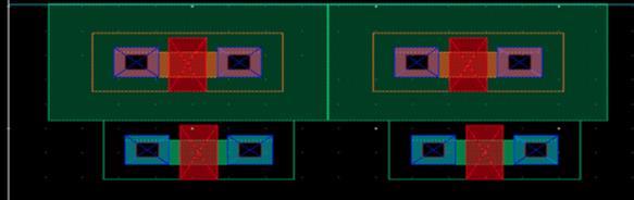
3 History of Layout Generation Layout: Each layer of each devices were drawn manually Layout L: PDKs offer pre-made scalable devices. pcells can be individually added to your layout. Layout XL: Generate layout from schematic (pcells Parametrized Cells)


4 Layout L and Layout XL File New Cell View Application / Open with choose Layout XL Hit -- Always use this application for this type of file
 Launch LayoutXL (In")
5 Layout L and Layout XL Tools Design Synthesis LayoutXL (In cadence 5) Launch LayoutXL (In cadence 6)

6 Layout L and Layout XL See the below menu
7 OUTLINE Introduction Mapping for Schematic and Layout Connectivity Generate Layout from Schematic Connectivity Some Useful Features Virtuoso Custom Placer and Router Some Layout Editing Tips

8 Mapping Launch Configure Physical Hierarchy Physical Library and Physical Cell should be set
9 Mapping If you have existing design, you can map with Connectivity Update Device Corresponding
10 OUTLINE Introduction Mapping for Schematic and Layout Connectivity Generate Layout from Schematic Connectivity Some Useful Features Virtuoso Custom Placer and Router Some Layout Editing Tips
11 Generating Layout From Schematic Connectivity Generate All from Source Connectivity Generate Pick from Schematic File Import XL Netlist (Generates from CDL)

12 Generating Layout From Schematic Change default pin layers to which layer you want Set pins from Create Label As Hit Ok, Cadence automatically creates and places the instances in your layout
13 Generating Layout From Schematic Shift - f
 Options Display Set Display level from 0 to 0 (Ctrl-")
14 Displaying Levels Options Display Set Display level from 0 to 32 (Shift - f) Options Display Set Display level from 0 to 0 (Ctrl- f)

15 Boundary Box Move the cells inside purple bounding box It is not necessary to use it If rules and constraints are entered, Cadence can do automatic routing, which is not optimal in most cases. Route Automatic Routing
16 OUTLINE Introduction Mapping for Schematic and Layout Connectivity Generate Layout from Schematic Connectivity Some Useful Features Virtuoso Custom Placer and Router Some Layout Editing Tips

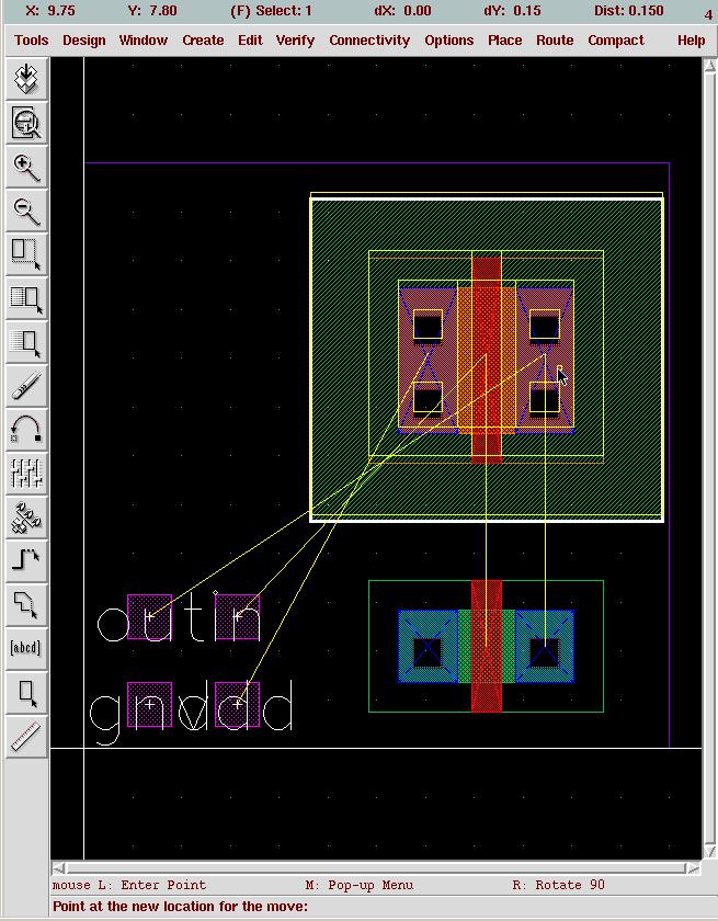
17 Connectivity When you select a device or a pin in schematic, it will be highlighted in layout

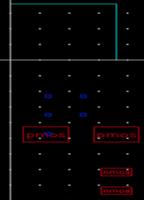
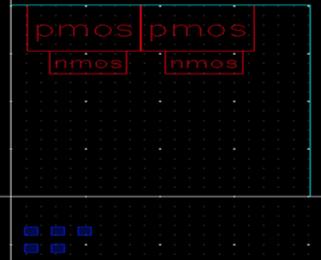
18 Connectivity Cell boundary Pins transistors

19 Connectivity Moving a device or a pin will show its connections with other devices
20 Connectivity
21 Connectivity
22 OUTLINE Introduction Mapping for Schematic and Layout Connectivity Generate Layout from Schematic Connectivity Some Useful Features Virtuoso Custom Placer and Router Some Layout Editing Tips
23 Design Rule Driven (DRD) Options DRD Edit Off Notify Enforce This is a kind of DRC during layout editing


24 Transistor Chaining Move transistor Flight Line will appear Drag the transistor from the highlighted side Vias will be aligned Chaining is achieved From Virtuoso XL Options, Auto Abutment needs to be turned on
25 Transistor Folding Edit Transistor Folding Specify the number of gates and width of each gate Split devices can automatically abutted Abutment can be done while moving devices
26 Permuting Pins & Swaping Devices Connectivity Permute Pins Allows pins of a p-cell device to be swapped Options Virtuoso XL turn on Auto Permute Edit Other Swap Components Swaps selected two components, does not swap connections
27 Aligning Devices Edit Other Align Align any object, instance, layer along its edge, origin or center Minimum separation distance can be applied This comment does not read design rules
28 Property Transistor properties Bulk Gate Fingers Drain/Source Edit Property or q Transistor parameters can be modified during editing layout
 Set drain/source connection")
29 Property Set bulk connection (left, right, dual, abutted, non-abutted) Set gate fingers connection (top, bottom, both, poly, metal) Set drain/source connection
 Create Guided routing ctrl + shift + g (creates guard rings) Route Automatic Routing Paths can be used with")
30 Creating Wires & Guard Rings Wire Create path - p Create shape r Create Point to point ctrl + shift +p Create Multipart Path (MPP creates contact arrays, guard rings, shielded wires) Create Guided routing ctrl + shift + g (creates guard rings) Route Automatic Routing Paths can be used with DRD

31 Creating Via Create Via O hot key
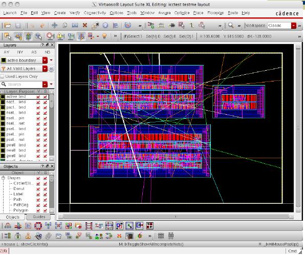
32 Incomplete Nets Connectivity Nets Show/Hide Selected Incomplete Nets

33 Creating Label Create Label l
34 OUTLINE Introduction Mapping for Schematic and Layout Connectivity Generate Layout from Schematic Connectivity Some Useful Features Virtuoso Custom Placer and Router Some Layout Editing Tips
35 Virtuoso Custom Placer & Router It needs placer.rul and router.rul rule files Boundary Box is needed Generally, it is not optimal

36 Virtuoso Custom Placer & Router

37 Virtuoso Custom Placer & Router Place Partitioning Name partitions Link to schematic Create rectangles for partitions Hit the Attach Shape

38 Virtuoso Custom Placer & Router Place Placement Planning Choose the Components Chose the Allign Components Calculate Estimate Will calculate the area of NMOS and PMOS in the boundary

39 Virtuoso Custom Placer & Router Place Placer Choose the Group CMOS Pairs Choose the Optimize Placement Click on Set file Select the rule file

40 Virtuoso Custom Placer & Router

41 Virtuoso Custom Placer & Router Route Export to Route Select Cadence chip assembly There may be some other router depending on your licenses

42 Virtuoso Custom Placer & Router AutoRoute Detail Router Detail Route Hit OK

43 Virtuoso Custom Placer & Router Auto route Clean Change number of passes Remove higher layer of metals Try until it seems fine

44 Virtuoso Custom Placer & Router Add NTAP and PTAP Create Instance Fill the # of rows and colums

45 Virtuoso Custom Placer & Router
46 OUTLINE Introduction Mapping for Schematic and Layout Connectivity Generate Layout from Schematic Connectivity Some Useful Features Virtuoso Custom Placer and Router Some Layout Editing Tips
47 Layout Editing Tips During layout editing try to use Mark/Unmark Nets Array Copy Chop the Line Split the Line Change the origin
48 Engineering Change Order (ECO) During layout editing Make required changes to the schematic Connectivity Check against Source (check the layout against the schematic, missing devices in the layout highlighted in schematic) Connectivity Update Components and Nets (updates the layout with new schematic connectivity, components and pins) Connectivity Update Layout parameters (updates the layout with new schematic parameters) Highlights old extra devices, place new devices, highlights wrong connections
49 References Cadence Automated Custom Physical Design Manual Cadence Tutorial of VLSI Research Group CACS, Chaitanya Emmela North Carolina State University Tutorials
EE115C Digital Electronic Circuits. Tutorial 4: Schematic-driven Layout (Virtuoso XL)
") EE115C Digital Electronic Circuits Tutorial 4: Schematic-driven Layout (Virtuoso XL) This tutorial will demonstrate schematic-driven layout on the example of a 2-input NAND gate. Simple Layout (that won
EE115C Digital Electronic Circuits Tutorial 4: Schematic-driven Layout (Virtuoso XL) This tutorial will demonstrate schematic-driven layout on the example of a 2-input NAND gate. Simple Layout (that won
TUTORIAL II ECE 555 / 755 Updated on September 11 th 2006 CADENCE LAYOUT AND PARASITIC EXTRACTION
 TUTORIAL II ECE 555 / 755 Updated on September 11 th 2006 CADENCE LAYOUT AND PARASITIC EXTRACTION After finishing a schematic of your design (Tutorial-I), the next step is creating masks which are for
UNIVERSITY OF WATERLOO
 UNIVERSITY OF WATERLOO UW ASIC DESIGN TEAM: Cadence Tutorial Description: Part I: Layout & DRC of a CMOS inverter. Part II: Extraction & LVS of a CMOS inverter. Part III: Post-Layout Simulation. The Cadence
Virtuoso Custom Design Platform GXL. Open Database. PDKs. Constraint Management. Customer IP
 Virtuoso Custom Design Platform GL The Cadence Virtuoso custom design platform is the industry s leading design system for complete front-to-back analog, RF, mixed-signal, and custom digital design. The
ECE471/571 Energy Efficient VLSI Design Project 2 Cadence Setup and Creation of an Inverter Due Date 11:30 am on Friday, February 2 nd, 2018
 ECE471/571 Energy Efficient VLSI Design Project 2 Cadence Setup and Creation of an Inverter Due Date 11:30 am on Friday, February 2 nd, 2018 Introduction This project will first walk you through the setup
Design rule illustrations for the AMI C5N process can be found at:
 Cadence Tutorial B: Layout, DRC, Extraction, and LVS Created for the MSU VLSI program by Professor A. Mason and the AMSaC lab group. Revised by C Young & Waqar A Qureshi -FS08 Document Contents Introduction
ECE471/571 Energy Ecient VLSI Design
 ECE471/571 Energy Ecient VLSI Design Project 2 Cadence Setup and Creation of an Inverter Due Date 11:30pm on Friday, January 30 th 2015 Introduction This project will rst walk you through the setup for
VLSI Lab Tutorial 3. Virtuoso Layout Editing Introduction
 VLSI Lab Tutorial 3 Virtuoso Layout Editing Introduction 1.0 Introduction The purpose of this lab tutorial is to guide you through the design process in creating a custom IC layout for your CMOS inverter
Virtuoso Schematic Composer
 is a schematic design tool from Cadence. In this tutorial you will learn how to put electrical components, make wire connections, insert pins and check for connection error. Start Cadence Custom IC Design
Amplifier Simulation Tutorial. Design Kit: Cadence 0.18μm CMOS PDK (gpdk180) (Cadence Version 6.1.5)
 (Cadence Version 6.1.5)") Amplifier Simulation Tutorial Design Kit: Cadence 0.18μm CMOS PDK (gpdk180) (Cadence Version 6.1.5) Yongsuk Choi, Marvin Onabajo This tutorial provides a quick introduction to the use of Cadence tools
Amplifier Simulation Tutorial Design Kit: Cadence 0.18μm CMOS PDK (gpdk180) (Cadence Version 6.1.5) Yongsuk Choi, Marvin Onabajo This tutorial provides a quick introduction to the use of Cadence tools
Virtuoso Layout Editor
 This tutorial will cover the basic steps involved in using the Cadence layout editor called Virtuoso, extracting layout, and running simulation on the layout. The inverter layout is used as an example
UNIVERSITY OF CALIFORNIA College of Engineering Department of Electrical Engineering and Computer Sciences Lab #2: Layout and Simulation
 UNIVERSITY OF CALIFORNIA College of Engineering Department of Electrical Engineering and Computer Sciences Lab #2: Layout and Simulation NTU IC541CA 1 Assumed Knowledge This lab assumes use of the Electric
EE 330 Laboratory 3 Layout, DRC, and LVS
 EE 330 Laboratory 3 Layout, DRC, and LVS Spring 2018 Contents Objective:... 2 Part 1 creating a layout... 2 1.1 Run DRC... 2 1.2 Stick Diagram to Physical Layer... 3 1.3 Bulk Connections... 3 1.4 Pins...
CMOS VLSI Design Lab 4: Full Chip Assembly
 CMOS VLSI Design Lab 4: Full Chip Assembly In this final lab, you will assemble and simulate your entire MIPS microprocessor! You will build your top level chip cell by connecting the datapath, aludec,
Lab 2. Standard Cell layout.
 Lab 2. Standard Cell layout. The purpose of this lab is to demonstrate CMOS-standard cell design. Use the lab instructions and the cadence manual (http://www.es.lth.se/ugradcourses/cadsys/cadence.html)
EE 330 Laboratory 3 Layout, DRC, and LVS Fall 2015
 EE 330 Laboratory 3 Layout, DRC, and LVS Fall 2015 Contents Objective:... 2 Part 1 Creating a layout... 2 1.1 Run DRC Early and Often... 2 1.2 Create N active and connect the transistors... 3 1.3 Vias...
EE 330 Spring 2018 Laboratory 2: Basic Boolean Circuits
 EE 330 Spring 2018 Laboratory 2: Basic Boolean Circuits Contents Objective:... 2 Part 1: Introduction... 2 Part 2 Simulation of a CMOS Inverter... 3 Part 2.1 Attaching technology information... 3 Part
Cadence Tutorial. Introduction to Cadence 0.18um, Implementation and Simulation of an inverter. A. Moradi, A. Miled et M. Sawan
 Cadence Tutorial Introduction to Cadence 0.18um, Implementation and Simulation of an inverter A. Moradi, A. Miled et M. Sawan Section 1: Introduction to Cadence You will see how to create a new library
DATASHEET VIRTUOSO LAYOUT SUITE FAMILY
 DATASHEET The Cadence Virtuoso Layout Suite family of products delivers a complete solution for front-to-back custom analog, digital, RF, and mixed-signal design. It preserves design intent throughout
EE434 ASIC & Digital Systems. From Layout to SPICE Simulation (Virtuoso, Calibre, HSpice) Spring 2017 Dae Hyun Kim
 Spring 2017 Dae Hyun Kim") EE434 ASIC & Digital Systems From Layout to SPICE Simulation (Virtuoso, Calibre, HSpice) Spring 2017 Dae Hyun Kim daehyun@eecs.wsu.edu 1 Preparation for Lab2 Download the following file into your working
EE434 ASIC & Digital Systems From Layout to SPICE Simulation (Virtuoso, Calibre, HSpice) Spring 2017 Dae Hyun Kim daehyun@eecs.wsu.edu 1 Preparation for Lab2 Download the following file into your working
Tutorial I: Cadence Innovus ECE6133: Physical Design Automation of VLSI Systems Georgia Institute of Technology Prof. Sung Kyu Lim
 Tutorial I: Cadence Innovus ECE6133: Physical Design Automation of VLSI Systems Georgia Institute of Technology Prof. Sung Kyu Lim I. Setup for Cadence Innovus 1. Copy the following files into your working
ESE 570 Cadence Lab Assignment 2: Introduction to Spectre, Manual Layout Drawing and Post Layout Simulation (PLS)
") ESE 570 Cadence Lab Assignment 2: Introduction to Spectre, Manual Layout Drawing and Post Layout Simulation (PLS) Objective Part A: To become acquainted with Spectre (or HSpice) by simulating an inverter,
ESE 570 Cadence Lab Assignment 2: Introduction to Spectre, Manual Layout Drawing and Post Layout Simulation (PLS) Objective Part A: To become acquainted with Spectre (or HSpice) by simulating an inverter,
ANALOG MICROELECTRONICS ( A)
") ANALOG MICROELECTRONICS (304-534A) IBM 130 nm CMOS Technology An Introduction to Cadence Virtuoso Layout Tool and the Analog Simulation Environment Prepared By - Azhar A. Chowdhury Updated by Ming Yang
ANALOG MICROELECTRONICS (304-534A) IBM 130 nm CMOS Technology An Introduction to Cadence Virtuoso Layout Tool and the Analog Simulation Environment Prepared By - Azhar A. Chowdhury Updated by Ming Yang
Process technology and introduction to physical
 Neuromorphic Engineering II Lab 3, Spring 2014 1 Lab 3 March 10, 2014 Process technology and introduction to physical layout Today you will start to learn to use the Virtuoso layout editor XL which is
Virtuoso Layout Suite XL
 Accelerated full custom IC layout Part of the Cadence Virtuoso Layout Suite family of products, is a connectivity- and constraint-driven layout environment built on common design intent. It supports custom
EECE 285 VLSI Design. Cadence Tutorial EECE 285 VLSI. By: Kevin Dick Co-author: Jeff Kauppila Co-author: Dr. Arthur Witulski
 Cadence Tutorial EECE 285 VLSI By: Kevin Dick Co-author: Jeff Kauppila Co-author: Dr. Arthur Witulski 1 Table of Contents Purpose of Cadence 1) The Purpose of Cadence pg. 4 Linux 1) The Purpose of Linux
Cadence Tutorial 2: Layout, DRC/LVS and Circuit Simulation with Extracted Parasitics
 Cadence Tutorial 2: Layout, DRC/LVS and Circuit Simulation with Extracted Parasitics Introduction This tutorial describes how to generate a mask layout in the Cadence Virtuoso Layout Editor. Use of DIVA
Cadence Virtuoso Schematic Design and Circuit Simulation Tutorial
 Cadence Virtuoso Schematic Design and Circuit Simulation Tutorial Introduction This tutorial is an introduction to schematic capture and circuit simulation for ENGN1600 using Cadence Virtuoso. These courses
Revision Notes: July2004 Generate tutorial for single transistor analysis. Based on existing schematic entry tutorial developed for ECE410
 Cadence Analog Tutorial 1: Schematic Entry and Transistor Characterization Created for the MSU VLSI program by Professor A. Mason and the AMSaC lab group. Revision Notes: July2004 Generate tutorial for
Laboratory 6. - Using Encounter for Automatic Place and Route. By Mulong Li, 2013
 CME 342 (VLSI Circuit Design) Laboratory 6 - Using Encounter for Automatic Place and Route By Mulong Li, 2013 Reference: Digital VLSI Chip Design with Cadence and Synopsys CAD Tools, Erik Brunvand Background
CADENCE SETUP. ECE4430-Analog IC Design
 CADENCE SETUP This short tutorial shows how to configure Cadence to use the NCSU Cadence Design Kit (CDK) with access to the ON Semiconductor C5 0.5-µm and the TSMC 0.35-µm CMOS processes libraries. In
Cadence Tutorial D: Using Design Variables and Parametric Analysis Document Contents Introduction Using Design Variables Apply Apply
 Cadence Tutorial D: Using Design Variables and Parametric Analysis Created for the MSU VLSI program by Casey Wallace Last Updated by: Patrick O Hara SS15 Document Contents Introduction Using Design Variables
DATASHEET VIRTUOSO LAYOUT SUITE GXL
 DATASHEET Part of the Cadence Virtuoso Layout Suite family of products, is a collection of fully automated layout capabilities such as custom placement and routing, layout optimization, module generation,
This is a brief tutorial about building a Symbol for a Schematic in Cadence IC design tool environment for hierarchical design of schematics.
 This is a brief tutorial about building a Symbol for a Schematic in Cadence IC design tool environment for hierarchical design of schematics. 1. > cd work035 2. > cadsetup ams035 3. > virtuoso& IMPORTANT:
VLSI Lab Tutorial 1. Cadence Virtuoso Schematic Composer Introduction
 VLSI Lab Tutorial 1 Cadence Virtuoso Schematic Composer Introduction 1.0 Introduction The purpose of the first lab tutorial is to help you become familiar with the schematic editor, Virtuoso Schematic
Cadence Tutorial A: Schematic Entry and Functional Simulation Created for the MSU VLSI program by Andrew Mason and the AMSaC lab group.
 Cadence Tutorial A: Schematic Entry and Functional Simulation Created for the MSU VLSI program by Andrew Mason and the AMSaC lab group. Revision Notes: Aug. 2003 update and edit A. Mason add intro/revision/contents
ELEC451 Integrated Circuit Engineering Using Cadence's Virtuoso Layout Editing Tool
 ELEC451 Integrated Circuit Engineering Using Cadence's Virtuoso Layout Editing Tool Contents Contents 1. General 2. Creating and Working On a Layout o 2.1 Undoing/Re-doing an Action o 2.2 Display Options
ASIC Physical Design Top-Level Chip Layout
 ASIC Physical Design Top-Level Chip Layout References: M. Smith, Application Specific Integrated Circuits, Chap. 16 Cadence Virtuoso User Manual Top-level IC design process Typically done before individual
CMOS INVERTER LAYOUT TUTORIAL
 PRINCESS SUMAYA UNIVERSITY FOR TECHNOLOGY CMOS INVERTER LAYOUT TUTORIAL We will start the inverter by drawing a PMOS. The first step is to draw a poly layer. Click on draw a rectangle and choose the poly
Select the technology library: NCSU_TechLib_ami06, then press OK.
 ECE 126 Inverter Tutorial: Schematic & Symbol Creation Created for GWU by Anis Nurashikin Nordin & Thomas Farmer Tutorial adapted from: http://www.ee.ttu.edu/ee/cadence/commondirectory/final%20tutorials/digitalcircuitsimulationusingvirtuoso.doc
More information can be found in the Cadence manuals Virtuoso Layout Editor User Guide and Cadence Hierarchy Editor User Guide.
 Chapter 6 Building with Layout This chapter consists of two parts. The first describes the generation of layout views and the second deals with the various tools used for verifying the layout, both physical
Microelectronica. Full-Custom Design with Cadence Tutorial
 Área Científica de Electrónica Microelectronica Full-Custom Design with Cadence Tutorial AustriaMicroSystems C35B3 (HIT-Kit 3.70) Marcelino Santos Table of contends 1. Starting Cadence... 3 Starting Cadence
EE115C Digital Electronic Circuits. Tutorial 2: Hierarchical Schematic and Simulation
 EE115C Digital Electronic Circuits Tutorial 2: Hierarchical Schematic and Simulation The objectives are to become familiar with Virtuoso schematic editor, learn how to create the symbol view of basic primitives,
DRC and LVS checks using Cadence Virtuoso Version 3.0
 DRC and LVS checks using Cadence Virtuoso Version 3.0 Start virtuoso l l Open a virtuoso session in the directory which contains the required cds.lib and lib.def files. Command : virtuoso & Open the layout
Fall 2008: EE5323 VLSI Design I using Cadence
 1 of 23 9/17/2008 6:47 PM Fall 2008: EE5323 VLSI Design I using Cadence This tutorial has been adapted from EE5323 offered in Fall 2007. Thanks to Jie Gu, Prof. Chris Kim and Satish Sivaswamy of the University
CPE/EE 427, CPE 527, VLSI Design I: Tutorial #2, Schematic Capture, DC Analysis, Transient Analysis (Inverter, NAND2)
") CPE/EE 427, CPE 527, VLSI Design I: Tutorial #2, Schematic Capture, DC Analysis, Transient Analysis (Inverter, NAND2) Joel Wilder, Aleksandar Milenkovic, ECE Dept., The University of Alabama in Huntsville
CPE/EE 427, CPE 527, VLSI Design I: Tutorial #2, Schematic Capture, DC Analysis, Transient Analysis (Inverter, NAND2) Joel Wilder, Aleksandar Milenkovic, ECE Dept., The University of Alabama in Huntsville
Cadence IC Design Manual
 Cadence IC Design Manual For EE5518 ZHENG Huan Qun Lin Long Yang Revised on May 2017 Department of Electrical & Computer Engineering National University of Singapore 1 P age Contents 1 INTRODUCTION...
Guide to the CSE 577 Lab and Cad tools
 Guide to the CSE 577 Lab and Cad tools 1. Introduction The objective of this tutorial is to give you an overview to (1) setup the Cadence and Synopsys hspice tools for your account in IST 218 Lab, (2)
CPE/EE 427, CPE 527, VLSI Design I: Tutorial #1, Full Custom VLSI (inverter layout)
") CPE/EE 427, CPE 527, VLSI Design I: Tutorial #1, Full Custom VLSI (inverter layout) Joel Wilder, Aleksandar Milenkovic, ECE Dept., The University of Alabama in Huntsville Adapted from Virginia Tech, Dept.
CPE/EE 427, CPE 527, VLSI Design I: Tutorial #1, Full Custom VLSI (inverter layout) Joel Wilder, Aleksandar Milenkovic, ECE Dept., The University of Alabama in Huntsville Adapted from Virginia Tech, Dept.
DOWNLOAD PDF CADENCE WAVEFORM CALCULATOR USER GUIDE
 Chapter 1 : CSE / Cadence Tutorial The Cadence Design Communities support Cadence users and technologists interacting to exchange ideas, news, technical information, and best practices to solve problems
FACULTY OF ENGINEERING MULTIMEDIA UNIVERSITY LAB SHEET DIGITAL INTEGRATED CIRCUIT
 FACULTY OF ENGINEERING MULTIMEDIA UNIVERSITY LAB SHEET DIGITAL INTEGRATED CIRCUIT DIC1: Schematic Design Entry, Simulation & Verification DIC2: Schematic Driven Layout Drawing (SDL) Design Rule Check (DRC)
Creating Verilog Tutorial Netlist Release Date: 01/13/2005(Version 2)
") Creating Verilog Tutorial 2-1 - Creating a verilog netlist for a schematic: The verilog netlist is necessary for automatic layout (placement and routing) tools. It contains information about the I/O pins
Creating Verilog Tutorial 2-1 - Creating a verilog netlist for a schematic: The verilog netlist is necessary for automatic layout (placement and routing) tools. It contains information about the I/O pins
Laker 3 Custom Design Tools
 Datasheet Laker 3 Custom Design Tools Laker 3 Custom Design Tools The Laker 3 Custom Design Tools form a unified front-to-back environment for custom circuit design and layout. They deliver a complete
TRANSISTOR-LEVEL ROUTING WITH IC CRAFTSMAN & VIRTUOSO USING A LOCAL INTERCONNECT
 TRANSISTOR-LEVEL ROUTING WITH IC CRAFTSMAN & VIRTUOSO USING A LOCAL INTERCONNECT TONY LAUNDRIE IC DESIGN ENGINEER P.O. BOX 4000 CHIPPEWA FALLS, WI 54729 atl@sgi.com INTERNATIONAL CADENCE USER GROUP CONFERENCE
Cadence Tutorial A: Schematic Entry and Functional Simulation Created for the MSU VLSI program by Professor A. Mason and the AMSaC lab group.
 Cadence Tutorial A: Schematic Entry and Functional Simulation Created for the MSU VLSI program by Professor A. Mason and the AMSaC lab group. Revision Notes: Jan. 2006 Updated for use with spectre simulator
CMOS Design Lab Manual
 CMOS Design Lab Manual Developed By University Program Team CoreEl Technologies (I) Pvt. Ltd. 1 Objective Objective of this lab is to learn the Mentor Graphics HEP2 tools as well learn the flow of the
ECE425: Introduction to VLSI System Design Machine Problem 3 Due: 11:59pm Friday, Dec. 15 th 2017
 ECE425: Introduction to VLSI System Design Machine Problem 3 Due: 11:59pm Friday, Dec. 15 th 2017 In this MP, you will use automated tools to synthesize the controller module from your MP2 project into
Layout and Layout Verification. of an Inverter Circuit
 Layout and Layout Verification of an Inverter Circuit Santa Clara University Department of Electrical Engineering By Piyush Panwar Under Guidance of Dr Samiha Mourad Date of Last Revision: August 7, 2010
EE5323/5324 VLSI Design I/II using Cadence
 1 of 18 2009-1-23 23:58 Spring 2009: EE5323/5324 VLSI Design I/II using Cadence This tutorial has been adapted from EE5323 offered in Fall 2007. Thanks to Jie Gu, Prof. Chris Kim and Satish Sivaswamy of
CS755 CAD TOOL TUTORIAL
 CS755 CAD TOOL TUTORIAL CREATING SCHEMATIC IN CADENCE Shi-Ting Zhou shi-ting@cs.wisc.edu After you have figured out what you want to design, and drafted some pictures and diagrams, it s time to input schematics
DRC and LVS checks using Cadence Virtuoso Version 2.0
 DRC and LVS checks using Cadence Virtuoso Version 2.0 Start virtuoso l l Open a virtuoso session in the directory which contains the required cds.lib and lib.def files. Command : virtuoso & Open the layout
Procedure for PCBoard Layout
 Procedure for PCBoard Layout Introduction The following 6 pages of instructions will take you step by step through the creation of your PCB using Orcad Layout. If you are planning to manually lay out your
SCHEMATIC1 SCHEMATIC2 SCHEMATIC1 SCHEMATIC2 SCHEMATIC3 PAGE1 PAGE2 PAGE3 PAGE1 PAGE1 PAGE2 PAGE1 PAGE1 PAGE2
 An OrCAD Tutorial Dr. S.S.Limaye 1. Introduction OrCAD is a suite of tools from Cadence company for the design and layout of printed circuit boards (PCBs). This is the most popular tool in the industry.
ACCELERATING CHIP-LEVEL ROUTING AND DESIGN
 ACCELERATING CHIP-LEVEL ROUTING AND DESIGN Johnny Premkumar National Semiconductor Corporation Johnny.Premkumar@nsc.com September 2005 ABSTRACT This paper focuses on optimizing and improving time to market
Laker Custom Layout Automation System
 The Laker Custom Layout offers powerful solutions for analog, mixed-signal, memory, and custom digital IC design that address key pain points in the layout process. The Laker layout system provides an
EEC 116 Fall 2011 Lab #1 Cadence Schematic Capture and Layout Tutorial
 EEC 116 Fall 2011 Lab #1 Cadence Schematic Capture and Layout Tutorial Dept. of Electrical and Computer Engineering University of California, Davis September 26, 2011 Reading: Rabaey Chapters 1, 2, A,
Cadence Virtuoso Layout Connectivity Mark- Net Tutorial
 Cadence Virtuoso Layout Connectivity Mark- Net Tutorial Digital VLSI Chip Design CAD manual addendum When you re drawing layout, especially of a complex cell, it s sometimes hard to see exactly what your
Tutorial for Cadence SOC Encounter Place & Route
 Tutorial for Cadence SOC Encounter Place & Route For Encounter RTL-to-GDSII System 13.15 T. Manikas, Southern Methodist University, 3/9/15 Contents 1 Preliminary Setup... 1 1.1 Helpful Hints... 1 2 Starting
Lab 4 LVS and Post layout Simulation
 Lab 4 LVS and Post layout Simulation Objective: In this lab you will learn 1. How to check if your layout that you drew in lab 3 matches your schematic that you drew in lab 2. 2. How to do the post layout
A Framework for Systematic Evaluation and Exploration of Design Rules
 A Framework for Systematic Evaluation and Exploration of Design Rules Rani S. Ghaida* and Prof. Puneet Gupta EE Dept., University of California, Los Angeles (rani@ee.ucla.edu), (puneet@ee.ucla.edu) Work
ESE570 Spring University of Pennsylvania Department of Electrical and System Engineering Digital Integrated Cicruits AND VLSI Fundamentals
 University of Pennsylvania Department of Electrical and System Engineering Digital Integrated Cicruits AND VLSI Fundamentals ESE570, Spring 2019 HW5: Delay and Layout Sunday, February 17th Due: Friday,
Expert Layout Editor. Technical Description
 Expert Layout Editor Technical Description Agenda Expert Layout Editor Overview General Layout Editing Features Technology File Setup Multi-user Project Library Setup Advanced Programmable Features Schematic
Tutorial on getting started in Cadence. Advanced Analog Circuits Spring 2015 Instructor: Prof. Harish Krishnaswamy TA: Jahnavi Sharma
 Tutorial on getting started in Cadence Advanced Analog Circuits Spring 2015 Instructor: Prof. Harish Krishnaswamy TA: Jahnavi Sharma Getting Started Start Cadence from the terminal by using the command
Lesson 12: Preparing for Post Processing
 12 Lesson 12: Preparing for Post Processing Learning Objectives In this lesson you will: Rename reference designators on the board design Backannotate changes made in the OrCAD and Allegro PCB Editor to
Exercise 1. Section 2. Working in Capture
 Exercise 1 Section 1. Introduction In this exercise, a simple circuit will be drawn in OrCAD Capture and a netlist file will be generated. Then the netlist file will be read into OrCAD Layout. In Layout,
Introduction to laboratory exercises in Digital IC Design.
 Introduction to laboratory exercises in Digital IC Design. A digital ASIC typically consists of four parts: Controller, datapath, memory, and I/O. The digital ASIC below, which is an FFT/IFFT co-processor,
EE 330 Laboratory Experiment Number 11
 EE 330 Laboratory Experiment Number 11 Design and Simulation of Digital Circuits using Hardware Description Languages Fall 2017 Contents Purpose:... 3 Background... 3 Part 1: Inverter... 4 1.1 Simulating
Creating LEF File. Abstract Generation: Creating LEF Tutorial File Release Date: 01/13/2004. Export GDS:
 Creating LEF Tutorial 1-1 - Creating LEF File Abstract Generation: Export GDS: Abstract generator comes as a part of the Silicon Ensemble package. As such, it cannot directly read ICFB library databases.
Spiral 2-8. Cell Layout
 2-8.1 Spiral 2-8 Cell Layout 2-8.2 Learning Outcomes I understand how a digital circuit is composed of layers of materials forming transistors and wires I understand how each layer is expressed as geometric
The Procedure for Laying out the inverter in TSMC s 0.35 micron Technogy using MOSIS SCMOS SCN4M_SUBM design rules.
 Page 1 of 5 CADENCE TUTORIAL Creating Layout of an inverter: click on File->library->new a Create Library form appears, fill it as follows: in the name field enter: inverter select "Attach to existing
Digital Integrated Circuits (83-313) Lecture 2: Technology and Standard Cell Layout
 Lecture 2: Technology and Standard Cell Layout") Digital Integrated Circuits (83-313) Lecture 2: Technology and Standard Cell Layout Semester B, 2016-17 Lecturer: Dr. Adam Teman TAs: Itamar Levi, Robert Giterman 26 March 2017 Disclaimer: This course
Digital Integrated Circuits (83-313) Lecture 2: Technology and Standard Cell Layout Semester B, 2016-17 Lecturer: Dr. Adam Teman TAs: Itamar Levi, Robert Giterman 26 March 2017 Disclaimer: This course
Place & Route: Using Silicon Ensemble
 Place & Route: Using Silicon Ensemble Introduction In a typical digital design flow, hardware description language is used to model a design and verify desired behavior. Once the desired functionality
Logging in, starting a shell tool, and starting the Cadence Tool Suite
 EEE 4134 VLSI I Laboratory Lab 0 (Introductory Lab) Logging into Cadence Server, Tool Setup, Cell Library Creation, Introduction to Custom IC Design flow Objectives: To login, start a shell tool and start
Orcad Layout Plus Tutorial
 Orcad Layout Plus Tutorial Layout Plus is a circuit board layout tool that accepts a layout-compatible circuit netlist (ex. from Capture CIS) and generates an output layout files that suitable for PCB
Full Custom Layout Optimization Using Minimum distance rule, Jogs and Depletion sharing
 Full Custom Layout Optimization Using Minimum distance rule, Jogs and Depletion sharing Umadevi.S #1, Vigneswaran.T #2 # Assistant Professor [Sr], School of Electronics Engineering, VIT University, Vandalur-
Cadence Tutorial C: Simulating DC and Timing Characteristics 1
 Cadence Tutorial C: Simulating DC and Timing Characteristics Created for the MSU VLSI program by Professor A. Mason and the AMSaC lab group Last updated by Patrick O Hara SS15 Document Contents Introduction
Physical Placement with Cadence SoCEncounter 7.1
 Physical Placement with Cadence SoCEncounter 7.1 Joachim Rodrigues Department of Electrical and Information Technology Lund University Lund, Sweden November 2008 Address for correspondence: Joachim Rodrigues
Single-Strip Static CMOS Layout
 EE244: Design Technology for Integrated Circuits and Systems Outline Lecture 6.2 Regular Module Structures CMOS Synthetic Libraries Weinberger Arrays Gate Matrix Programmable Logic Array (PLA) Storage
Creating a PCB Design with OrCAD PCB Editor
 Creating a PCB Design with OrCAD PCB Editor This guide is focused on learning how to create a PCB (Printed Circuit board) design. The guide will make use of the PCB Flow menu that is part of this workshop
AMS DESIGN METHODOLOGY
 OVER VIEW CADENCE ANALOG/ MIXED-SIGNAL DESIGN METHODOLOGY The Cadence Analog/Mixed-Signal (AMS) Design Methodology employs advanced Cadence Virtuoso custom design technologies and leverages silicon-accurate
Lab. Course Goals. Topics. What is VLSI design? What is an integrated circuit? VLSI Design Cycle. VLSI Design Automation
 Course Goals Lab Understand key components in VLSI designs Become familiar with design tools (Cadence) Understand design flows Understand behavioral, structural, and physical specifications Be able to
Tutorial II: Cadence Virtuoso ECE6133: Physical Design Automation of VLSI Systems Georgia Institute of Technology Prof.
 Tutorial II: Cadence Virtuoso ECE6133: Physical Design Automation of VLSI Systems Georgia Institute of Technology Prof. Sung Kyu Lim I. Setup for Cadence Virtuoso 1. Copy the following files into your
Introduction to Design Architect
 SANTA CLARA UNIVERSITY Dept. of Electrical Engineering Mentor Graphics Tutorials Introduction to Design Architect Yiching Chen Sangeetha Raman S. Krishnan I. Introduction II. This document contains a step-by-step
Using OrCAD Layout Plus A Simple Guide
 Using OrCAD Layout Plus A Simple Guide Written by Jose Cabral September 2006 Revised by Nithin Raghunathan 1 SKETCH THE CIRCUIT YOU WISH TO LAYOUT SKETCH THE LAYOUT COM J1 OUTPUT +12 COM -12 COM INPUT
Complete Tutorial (Includes Schematic & Layout)
") Complete Tutorial (Includes Schematic & Layout) Download 1. Go to the "Download Free PCB123 Software" button or click here. 2. Enter your e-mail address and for your primary interest in the product. (Your
Complete Tutorial (Includes Schematic & Layout) Download 1. Go to the "Download Free PCB123 Software" button or click here. 2. Enter your e-mail address and for your primary interest in the product. (Your
Galaxy Custom Designer LE Custom Layout Editing
 Datasheet Galaxy Custom Designer LE Custom Layout Editing Overview Galaxy Custom Designer LE is the modern-era choice for layout entry and editing, enabling users to meet the challenges of today s fast-moving
Synopsys Custom Designer Tutorial for a chip integra7on using the University of Utah Standard Cell Libraries In ON Semiconductor 0.
 Synopsys Custom Designer Tutorial for a chip integra7on using the University of Utah Standard Cell Libraries In ON Semiconductor 0.5u C5 CMOS Version 6.0 Overview This tutorial will take you through the
Microwave Office Training
 Microwave Office Training Schematic Layout Schematic Layout Schematic View Circuit We are Here! Schematic Layout View External World Need Export Mapping Two views of the same circuit! - including connectivity
Comprehensive Place-and-Route Platform Olympus-SoC
 Comprehensive Place-and-Route Platform Olympus-SoC Digital IC Design D A T A S H E E T BENEFITS: Olympus-SoC is a comprehensive netlist-to-gdsii physical design implementation platform. Solving Advanced
Can Recursive Bisection Alone Produce Routable Placements?
 Supported by Cadence Can Recursive Bisection Alone Produce Routable Placements? Andrew E. Caldwell Andrew B. Kahng Igor L. Markov http://vlsicad.cs.ucla.edu Outline l Routability and the placement context