Automatic Stress Effects Computation Based On A Layout Generation Tool For Analog IC
|
|
|
- Madison Suzan McDowell
- 5 years ago
- Views:
Transcription
1 2010 IEEE International Behavioral Modeling and Simulation Conference Modeling for Physical Design Session Automatic Stress Effects Computation Based On A Layout Generation Tool For Analog IC Stephanie YOUSSEF Damien DUPUIS Ramy ISKANDER Marie Minerve i LOUERAT LIP6 Laboratory, Université Pierre et Marie Curie, Paris, France
2 Plan Introduction : a. Problem definition b. Proposed design flow Stress effect modeling for CMOS transistors devices Results Conclusion 1
3 1. Introduction Traditional design Flow Description: i Disadvantages: An iterative process Manual design Flow High number of iterations Several steps supported by different tools Time Consuming Subject to human errors Automatic Stress Effects Computation Based On A Layout Generation Tool For Analog IC 2 1
4 1.a. Problem Definition Folding technique a. Electrical view b. Physical view Parasitic capacitance and gate resistance Inverse narrow width effect: Wf, Doping, Vth so IDS Aligned W to be on the physical grid Strong link between Layout and performance! 3 2
 Too complicated for design using the")

5 1.a. Problem Definition STI (Shallow Trench Isolation) Too complicated for design using the traditional flow! Automatic Stress Effects Computation Based On A Layout Generation Tool For Analog IC 4 3
6 1.b. Proposed design flow Proposed design flow Spec Techno. Sizing Layout generation Performance ok? Final Layout Goals : Internal lloop: Speed up the design flow. Minimize possible errors. Provide a two ways communication between the sizing and layout generation. Strongly coupling between layout and sizing Repeated several times. With minimal designer intervention. Automatic Stress Effects Computation Based On A Layout Generation Tool For Analog IC 4 5
. Provides a Customizable, Deformable and Reusable Layout.")
7 1.b. Proposed design flow Contributions of the proposed design flow Supports fast and accurate methods for parasitic calculations. Supports different layout styles for each device. Layout portable over different technologies. Supports Python description for the layout (ease of the modifications for the layout code). Provides a Customizable, Deformable and Reusable Layout. Automatic Stress Effects Computation Based On A Layout Generation Tool For Analog IC 6 5
 > 0.")
 > 7, NbDummies = The number of dummies at each stack s end > 1 ) Example :")
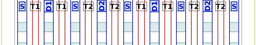
8 Stack Object Goal = Deformable and reusable layout. Python code. createstack( 2.Stress effect modeling for CMOS Type = type of the transistor t NMOS or PMOS > NMOS, W = The overall width of the transistor > 2 µ.m., L = The length of each finger (except dummies) > 0.15 µ.m., NFS = The number of stack s fingers (including dummies) > 7, NbDummies = The number of dummies at each stack s end > 1 ) Example : 65 n.m technology and BSIM4 model : Automatic Stress Effects Computation Based On A Layout Generation Tool For Analog IC 7 6
9 2.Stress effect modeling for CMOS Distance values provided by the stack object STI parameters such as SA and SB depends on (DMCI, DGI, DGG) Mismatch(DMCI, DMCG, ) Can add any other geometrical distances information Automatic Stress Effects Computation Based On A Layout Generation Tool For Analog IC 7 8
10 2.Stress effect modeling for CMOS Stress effect computation Considering a stack S 9

11 2.Stress effect modeling for CMOS BSIM4 model : Transistor stress effects One Folded transistor in a single stack Stress 10 Automatic Stress Effects Computation Based On A Layout Generation Tool For Analog IC 8
12 Automatically generated curves Technology = 65 nm, W= 6 µm and L = 0.15 µm 2.Stress effect modeling for CMOS One Folded transistor in a single stack 11 Automatic Stress Effects Computation Based On A Layout Generation Tool For Analog IC 9
13 2.Stress effect modeling for CMOS Stress and folding effects impact on current For a same large W= 6 µm and L = 0.15 µm: 1. Stress : NF = 1 with stress effects > Maximum effect NF = 1 without stress effects 2. Folding: NF = 50 for a large range NF = 1 without stress effects 12 Automatic Stress Effects Computation Based On A Layout Generation Tool For Analog IC 9

14 2.Stress effect modeling for CMOS Comparaison between stress and folding effects We must take into consideration the two effects! 13 Automatic Stress Effects Computation Based On A Layout Generation Tool For Analog IC 11
15 2.Stress effect modeling for CMOS Reducing the stress effects by increasing NF NF (SA_eff and SB_eff) Stress Error Automatic Stress Effects Computation Based On A Layout Generation Tool For Analog IC 12 14
16 2.Stress effect modeling for CMOS Reducing the stress effects by adding dummies Number of dummies Folding = Stress Error Surface Tradeoff between performance and surface! 15


17 2.Stress effect modeling for CMOS Mismatchproblem betweentwotransistors two transistors Differential pair example: Dedicated Layout Styles to reduce the mismatch h! 16


18 2.Stress effect modeling for CMOS Calculations of the stress effect parameters i = Tow Folded transistors in a single stack 17


19 Differential Pair symmetrical style 3 Results Technology = 65 nm, W= 6 µm and L = 0.06 µm, NF =
20 3 Results a. (1/α) v.s NF generation curves b. Current error simulation curves Different stress and error for the two transistors! 19 17


21 DifferentialPair interdigitatedstyle 3 Results Technology = 65 nm, W= 6 µm and L = 0.06 µm, NF = 4 20
22 3 Results a. (1/α) v.s NF generation curves b. Current error simulation curves Same stress and error for the two transistors! In nanometer technologies Interdigitated style is preferred! 21
23 4 Conclusion Conclusion We proposed a design flow to generate layouts for nanometers devices A Python API has been extended to compute stress effects Combined effects of stress and folding have been investigated The proposed flow has been successfully used to characterize dff different layout styles Show that the technology impact on the layout style choice Future work will focus on creating portable devices and integrating more nanometer effects 22
Taming the Challenges of 20nm Custom/Analog Design
 Taming the Challenges of 20nm Custom/Analog Design Custom and analog designers will lay the foundation for 20nm IC design. However, they face many challenges that arise from manufacturing complexity. The
SCHEMATIC PCELLS, FUTURE OF DEEP SUBMICRON CUSTOM IC DESIGN. PRANAV BHUSHAN CADENCE DESIGN SYSTEMS INC
 SCHEMATIC PCELLS, FUTURE OF DEEP SUBMICRON CUSTOM IC DESIGN PRANAV BHUSHAN CADENCE DESIGN SYSTEMS INC. +91-120-2562842 pbhushan@cadence.com RAJ ARUMUGAM QUALCOMM INC. +1-858-845-7877 rarumuga@qualcomm.com
A Review Paper on Reconfigurable Techniques to Improve Critical Parameters of SRAM
 IJSRD - International Journal for Scientific Research & Development Vol. 4, Issue 09, 2016 ISSN (online): 2321-0613 A Review Paper on Reconfigurable Techniques to Improve Critical Parameters of SRAM Yogit
Digital Integrated Circuits (83-313) Lecture 2: Technology and Standard Cell Layout
 Lecture 2: Technology and Standard Cell Layout") Digital Integrated Circuits (83-313) Lecture 2: Technology and Standard Cell Layout Semester B, 2016-17 Lecturer: Dr. Adam Teman TAs: Itamar Levi, Robert Giterman 26 March 2017 Disclaimer: This course
Digital Integrated Circuits (83-313) Lecture 2: Technology and Standard Cell Layout Semester B, 2016-17 Lecturer: Dr. Adam Teman TAs: Itamar Levi, Robert Giterman 26 March 2017 Disclaimer: This course
HIGH SPEED TDI EMBEDDED CCD IN CMOS SENSOR
 HIGH SPEED TDI EMBEDDED CCD IN CMOS SENSOR P. Boulenc 1, J. Robbelein 1, L. Wu 1, L. Haspeslagh 1, P. De Moor 1, J. Borremans 1, M. Rosmeulen 1 1 IMEC, Kapeldreef 75, B-3001 Leuven, Belgium Email: pierre.boulenc@imec.be,
Agilent 85194K IC-CAP BSIM4 Modeling Package
 Agilent 85194K IC-CAP BSIM4 Modeling Package Technical Overview The BSIM4 Modeling Package The BSIM4 Modeling Package offers a complete DC-to-RF CMOS modeling toolkit for U.C. Berkeley s BSIM4 model. Developed
Model Builder Program (MBP) Complete Silicon Turnkey Device Modeling Software
 Complete Silicon Turnkey Device Modeling Software") Model Builder Program (MBP) Complete Silicon Turnkey Device Modeling Software Introduction Model Builder Program (MBP) is a complete modeling solution that integrates SPICE simulation, model parameter
Model Builder Program (MBP) Complete Silicon Turnkey Device Modeling Software Introduction Model Builder Program (MBP) is a complete modeling solution that integrates SPICE simulation, model parameter
A Transistor-level Symmetrical Layout Generation for Analog Device
 R2-21 SASIMI 2012 Proceedings A Transistor-level Symmetrical Layout Generation for Analog Device Bo Yang, Qing Dong, Jing Li, Shigetoshi Nakatake Department of Information and Media Engineering, The University
Virtuoso Schematic Composer
 is a schematic design tool from Cadence. In this tutorial you will learn how to put electrical components, make wire connections, insert pins and check for connection error. Start Cadence Custom IC Design
Lecture 4a. CMOS Fabrication, Layout and Simulation. R. Saleh Dept. of ECE University of British Columbia
 Lecture 4a CMOS Fabrication, Layout and Simulation R. Saleh Dept. of ECE University of British Columbia res@ece.ubc.ca 1 Fabrication Fabrication is the process used to create devices and wires. Transistors
EE 330 Spring 2018 Laboratory 2: Basic Boolean Circuits
 EE 330 Spring 2018 Laboratory 2: Basic Boolean Circuits Contents Objective:... 2 Part 1: Introduction... 2 Part 2 Simulation of a CMOS Inverter... 3 Part 2.1 Attaching technology information... 3 Part
Introduction to laboratory exercises in Digital IC Design.
 Introduction to laboratory exercises in Digital IC Design. A digital ASIC typically consists of four parts: Controller, datapath, memory, and I/O. The digital ASIC below, which is an FFT/IFFT co-processor,
Latches SEU en techno IBM 130nm pour SLHC/ATLAS. CPPM, Université de la méditerranée, CNRS/IN2P3, Marseille, France
 Latches SEU en techno IBM 130nm pour SLHC/ATLAS CPPM, Université de la méditerranée, CNRS/IN2P3, Marseille, France Outline Introduction Description of the DICE latch Different implemented layouts for the
Methodology on Extracting Compact Layout Rules for Latchup Prevention in Deep-Submicron Bulk CMOS Technology
 IEEE TRANSACTIONS ON SEMICONDUCTOR MANUFACTURING, VOL. 16, NO. 2, MAY 2003 319 Methodology on Extracting Compact Layout Rules for Latchup Prevention in Deep-Submicron Bulk CMOS Technology Ming-Dou Ker,
International Training Workshop on FPGA Design for Scientific Instrumentation and Computing November 2013
 2499-13 International Training Workshop on FPGA Design for Scientific Instrumentation and Computing 11-22 Digital CMOS Design Combinational and sequential circuits, contd. Pirouz Bazargan-Sabet Department
Chapter 1: Measurement and Extraction of BSIM4 Model Parameters
 1: Measurement and Extraction of BSIM4 Model Parameters The following section summarizes some aspects of UCB s BSIM4 Model and Agilent s IC-CAP Modeling Package to measure and extract BSIM4 model parameters.
ESD Protection Design With Low-Capacitance Consideration for High-Speed/High- Frequency I/O Interfaces in Integrated Circuits
 Recent Patents on Engineering 2007, 1, 000-000 1 ESD Protection Design With Low-Capacitance Consideration for High-Speed/High- Frequency I/O Interfaces in Integrated Circuits Ming-Dou Ker* and Yuan-Wen
Circuits. L3: Fabrication and Layout -1 ( ) B. Mazhari Dept. of EE, IIT Kanpur. B. Mazhari, IITK. G-Number
 B. Mazhari Dept. of EE, IIT Kanpur. B. Mazhari, IITK. G-Number") EE60: CMOS Analog Circuits L: Fabrication and Layout - (8.8.0) B. Mazhari Dept. of EE, IIT Kanpur Suppose we have a Silicon wafer which is P-type and we wish to create a region within it which is N-type
EE60: CMOS Analog Circuits L: Fabrication and Layout - (8.8.0) B. Mazhari Dept. of EE, IIT Kanpur Suppose we have a Silicon wafer which is P-type and we wish to create a region within it which is N-type
ESD Protection Design for Mixed-Voltage I/O Interfaces -- Overview
 ESD Protection Design for Mixed-Voltage Interfaces -- Overview Ming-Dou Ker and Kun-Hsien Lin Abstract Electrostatic discharge (ESD) protection design for mixed-voltage interfaces has been one of the key
On the Design of Ultra-High Density 14nm Finfet based Transistor-Level Monolithic 3D ICs
 2016 IEEE Computer Society Annual Symposium on VLSI On the Design of Ultra-High Density 14nm Finfet based Transistor-Level Monolithic 3D ICs Jiajun Shi 1,2, Deepak Nayak 1,Motoi Ichihashi 1, Srinivasa
UNIVERSITY OF WATERLOO
 UNIVERSITY OF WATERLOO UW ASIC DESIGN TEAM: Cadence Tutorial Description: Part I: Layout & DRC of a CMOS inverter. Part II: Extraction & LVS of a CMOS inverter. Part III: Post-Layout Simulation. The Cadence
ESE 570 Cadence Lab Assignment 2: Introduction to Spectre, Manual Layout Drawing and Post Layout Simulation (PLS)
") ESE 570 Cadence Lab Assignment 2: Introduction to Spectre, Manual Layout Drawing and Post Layout Simulation (PLS) Objective Part A: To become acquainted with Spectre (or HSpice) by simulating an inverter,
ESE 570 Cadence Lab Assignment 2: Introduction to Spectre, Manual Layout Drawing and Post Layout Simulation (PLS) Objective Part A: To become acquainted with Spectre (or HSpice) by simulating an inverter,
A Design Tradeoff Study with Monolithic 3D Integration
 A Design Tradeoff Study with Monolithic 3D Integration Chang Liu and Sung Kyu Lim Georgia Institute of Techonology Atlanta, Georgia, 3332 Phone: (44) 894-315, Fax: (44) 385-1746 Abstract This paper studies
CMOS Process Flow. Layout CAD Tools
 CMOS Process Flow See supplementary power point file for animated CMOS process flow (see class ece410 website and/or* http://www.multimedia.vt.edu/ee5545/): This file should be viewed as a slide show It
Introduction 1. GENERAL TRENDS. 1. The technology scale down DEEP SUBMICRON CMOS DESIGN
 1 Introduction The evolution of integrated circuit (IC) fabrication techniques is a unique fact in the history of modern industry. The improvements in terms of speed, density and cost have kept constant
Electromagnetic Compatibility ( EMC )
") Electromagnetic Compatibility ( EMC ) ESD Strategies in IC and System Design 8-1 Agenda ESD Design in IC Level ( ) Design Guide Lines CMOS Design Process Level Method Circuit Level Method Whole Chip Design
Electromagnetic Compatibility ( EMC ) ESD Strategies in IC and System Design 8-1 Agenda ESD Design in IC Level ( ) Design Guide Lines CMOS Design Process Level Method Circuit Level Method Whole Chip Design
TUTORIAL II ECE 555 / 755 Updated on September 11 th 2006 CADENCE LAYOUT AND PARASITIC EXTRACTION
 TUTORIAL II ECE 555 / 755 Updated on September 11 th 2006 CADENCE LAYOUT AND PARASITIC EXTRACTION After finishing a schematic of your design (Tutorial-I), the next step is creating masks which are for
Design rule illustrations for the AMI C5N process can be found at:
 Cadence Tutorial B: Layout, DRC, Extraction, and LVS Created for the MSU VLSI program by Professor A. Mason and the AMSaC lab group. Revised by C Young & Waqar A Qureshi -FS08 Document Contents Introduction
PAPER MOS-Bounded Diodes for On-Chip ESD Protection in Deep Submicron CMOS Process
 IEICE TRANS. ELECTRON., VOL.E88 C, NO.3 MARCH 2005 429 PAPER MOS-Bounded Diodes for On-Chip ESD Protection in Deep Submicron CMOS Process Ming-Dou KER a), Kun-Hsien LIN, and Che-Hao CHUANG, Nonmembers
High-Performance Full Adders Using an Alternative Logic Structure
 Term Project EE619 High-Performance Full Adders Using an Alternative Logic Structure by Atulya Shivam Shree (10327172) Raghav Gupta (10327553) Department of Electrical Engineering, Indian Institure Technology,
CMOS INVERTER LAYOUT TUTORIAL
 PRINCESS SUMAYA UNIVERSITY FOR TECHNOLOGY CMOS INVERTER LAYOUT TUTORIAL We will start the inverter by drawing a PMOS. The first step is to draw a poly layer. Click on draw a rectangle and choose the poly
Amplifier Simulation Tutorial. Design Kit: Cadence 0.18μm CMOS PDK (gpdk180) (Cadence Version 6.1.5)
 (Cadence Version 6.1.5)") Amplifier Simulation Tutorial Design Kit: Cadence 0.18μm CMOS PDK (gpdk180) (Cadence Version 6.1.5) Yongsuk Choi, Marvin Onabajo This tutorial provides a quick introduction to the use of Cadence tools
Amplifier Simulation Tutorial Design Kit: Cadence 0.18μm CMOS PDK (gpdk180) (Cadence Version 6.1.5) Yongsuk Choi, Marvin Onabajo This tutorial provides a quick introduction to the use of Cadence tools
Investigation of the Gate-Driven Effect and Substrate-Triggered Effect on ESD Robustness of CMOS Devices
 190 IEEE TRANSACTIONS ON DEVICE AND MATERIALS RELIABILITY, VOL. 1, NO. 4, DECEMBER 2002 Investigation of the Gate-Driven Effect and Substrate-Triggered Effect on ESD Robustness of CMOS Devices Tung-Yang
Power dissipation! The VLSI Interconnect Challenge. Interconnect is the crux of the problem. Interconnect is the crux of the problem.
 The VLSI Interconnect Challenge Avinoam Kolodny Electrical Engineering Department Technion Israel Institute of Technology VLSI Challenges System complexity Performance Tolerance to digital noise and faults
QUEST 3D RLCG Extraction Depending on Frequency. RF Structures Parasitic Extractor
 QUEST 3D RLCG Extraction Depending on Frequency RF Structures Parasitic Extractor Introduction Type of Simulation Inputs / Outputs Graphical Interface Technology Process Layout Field Solver Output DOE
Novel silicon-controlled rectifier (SCR) for digital and high-voltage ESD power supply clamp
 for digital and high-voltage ESD power supply clamp") . BRIEF REPORT. SCIENCE CHINA Information Sciences February 2014, Vol. 57 029401:1 029401:6 doi: 10.1007/s11432-013-5016-1 Novel silicon-controlled rectifier (SCR) for digital and high-voltage ESD power
. BRIEF REPORT. SCIENCE CHINA Information Sciences February 2014, Vol. 57 029401:1 029401:6 doi: 10.1007/s11432-013-5016-1 Novel silicon-controlled rectifier (SCR) for digital and high-voltage ESD power
Power IC 용 ESD 보호기술. 구용서 ( Yong-Seo Koo ) Electronic Engineering Dankook University, Korea
 Electronic Engineering Dankook University, Korea") Power IC 용 ESD 보호기술 구용서 ( Yong-Seo Koo ) Electronic Engineering Dankook University, Korea yskoo@dankook.ac.kr 031-8005-3625 Outline Introduction Basic Concept of ESD Protection Circuit ESD Technology Issue
Power IC 용 ESD 보호기술 구용서 ( Yong-Seo Koo ) Electronic Engineering Dankook University, Korea yskoo@dankook.ac.kr 031-8005-3625 Outline Introduction Basic Concept of ESD Protection Circuit ESD Technology Issue
CHAPTER 3 SIMULATION TOOLS AND
 CHAPTER 3 SIMULATION TOOLS AND Simulation tools used in this simulation project come mainly from Integrated Systems Engineering (ISE) and SYNOPSYS and are employed in different areas of study in the simulation
Chapter 2 On-Chip Protection Solution for Radio Frequency Integrated Circuits in Standard CMOS Process
 Chapter 2 On-Chip Protection Solution for Radio Frequency Integrated Circuits in Standard CMOS Process 2.1 Introduction Standard CMOS technologies have been increasingly used in RF IC applications mainly
EE 330 Spring Laboratory 2: Basic Boolean Circuits
 EE 330 Spring 2013 Laboratory 2: Basic Boolean Circuits Objective: The objective of this experiment is to investigate methods for evaluating the performance of Boolean circuits. Emphasis will be placed
Electrostatic Discharge Implantation to Improve Machine-Model ESD Robustness of Stacked NMOS in Mixed-Voltage I/O Interface Circuits
 Electrostatic Discharge Implantation to Improve Machine-Model ESD Robustness of Stacked NMOS in Mixed-Voltage I/O Interface Circuits Ming-Dou Ker, Hsin-Chyh Hsu, and Jeng-Jie Peng * Nanoelectronics and
Low-Power SRAM and ROM Memories
 Low-Power SRAM and ROM Memories Jean-Marc Masgonty 1, Stefan Cserveny 1, Christian Piguet 1,2 1 CSEM, Neuchâtel, Switzerland 2 LAP-EPFL Lausanne, Switzerland Abstract. Memories are a main concern in low-power
Design and Simulation of Low Power 6TSRAM and Control its Leakage Current Using Sleepy Keeper Approach in different Topology
 Vol. 3, Issue. 3, May.-June. 2013 pp-1475-1481 ISSN: 2249-6645 Design and Simulation of Low Power 6TSRAM and Control its Leakage Current Using Sleepy Keeper Approach in different Topology Bikash Khandal,
TABLE OF CONTENTS 1.0 PURPOSE INTRODUCTION ESD CHECKS THROUGHOUT IC DESIGN FLOW... 2
 TABLE OF CONTENTS 1.0 PURPOSE... 1 2.0 INTRODUCTION... 1 3.0 ESD CHECKS THROUGHOUT IC DESIGN FLOW... 2 3.1 PRODUCT DEFINITION PHASE... 3 3.2 CHIP ARCHITECTURE PHASE... 4 3.3 MODULE AND FULL IC DESIGN PHASE...
TOPIC : Verilog Synthesis examples. Module 4.3 : Verilog synthesis
 TOPIC : Verilog Synthesis examples Module 4.3 : Verilog synthesis Example : 4-bit magnitude comptarator Discuss synthesis of a 4-bit magnitude comparator to understand each step in the synthesis flow.
CHARGED DEVICE MODEL ELECTROSTATIC DISCHARGE FAILURES IN SYSTEM ON A CHIP AND SYSTEM IN A PACKAGE DESIGNS NICHOLAS ALLEN OLSON DISSERTATION
 CHARGED DEVICE MODEL ELECTROSTATIC DISCHARGE FAILURES IN SYSTEM ON A CHIP AND SYSTEM IN A PACKAGE DESIGNS BY NICHOLAS ALLEN OLSON DISSERTATION Submitted in partial fulfillment of the requirements for the
Ecole Polytechnique Fédérale de Lausanne EPFL GigaRadMOST Total Ionizing Dose Effects on 28 nm Bulk CMOS Technology
 Ecole Polytechnique Fédérale de Lausanne EPFL GigaRadMOST Total Ionizing Dose Effects on 28 nm Bulk CMOS Technology Chun-Min Zhang, Farzan Jazaeri, Alessandro Pezzotta, Christian Enz Integrated Circuits
A Framework for Systematic Evaluation and Exploration of Design Rules
 A Framework for Systematic Evaluation and Exploration of Design Rules Rani S. Ghaida* and Prof. Puneet Gupta EE Dept., University of California, Los Angeles (rani@ee.ucla.edu), (puneet@ee.ucla.edu) Work
Moore s s Law, 40 years and Counting
 Moore s s Law, 40 years and Counting Future Directions of Silicon and Packaging Bill Holt General Manager Technology and Manufacturing Group Intel Corporation InterPACK 05 2005 Heat Transfer Conference
ECEN 474 Homework #2 Notes
 ECEN 474 Homework #2 Notes February 22, 2018 Due: 3-6-2018, 5:00PM Homeworks will not be received after due. Instructor: Sam Palermo 1. (50 points) Technology Characterization for Design In this problem,
VLSI Lab Tutorial 3. Virtuoso Layout Editing Introduction
 VLSI Lab Tutorial 3 Virtuoso Layout Editing Introduction 1.0 Introduction The purpose of this lab tutorial is to guide you through the design process in creating a custom IC layout for your CMOS inverter
Lecture 5. Other Adder Issues
 Lecture 5 Other Adder Issues Mark Horowitz Computer Systems Laboratory Stanford University horowitz@stanford.edu Copyright 24 by Mark Horowitz with information from Brucek Khailany 1 Overview Reading There
Cadence Virtuoso Schematic Design and Circuit Simulation Tutorial
 Cadence Virtuoso Schematic Design and Circuit Simulation Tutorial Introduction This tutorial is an introduction to schematic capture and circuit simulation for ENGN1600 using Cadence Virtuoso. These courses
Circuits Multi-Projets
 Circuits Multi-Projets Technology Processes & Runs in 2017 MPW Service Center for ICs, Photonics, & MEMS Prototyping & Low Volume Production http://mycmp.fr Grenoble - France Available Processes Process
ESD Protection Scheme for I/O Interface of CMOS IC Operating in the Power-Down Mode on System Board
 ESD Protection Scheme for I/O Interface of CMOS IC Operating in the Power-Down Mode on System Board Kun-Hsien Lin and Ming-Dou Ker Nanoelectronics and Gigascale Systems Laboratory Institute of Electronics,
SOI REQUIRES BETTER THAN IR-DROP. F. Clément, CTO
 SOI REQUIRES BETTER THAN IR-DROP F. Clément, CTO Content IR Drop Vs. System-level Interferences CWS Expertise Accuracy and Performance Silicon Validation Conclusion Copyright CWS 2004-2016 2 Sensitive
Microelectronics Reliability
 Microelectronics Reliability 53 (2013) 208 214 Contents lists available at SciVerse ScienceDirect Microelectronics Reliability journal homepage: www.elsevier.com/locate/microrel PMOS-based power-rail ESD
EE 471: Transport Phenomena in Solid State Devices
 EE 471: Transport Phenomena in Solid State Devices HW7 Due: 4/17/18 For this homework, you will download a free PC version of the industry standard SPICE circuit simulator called LTspice, provided by Linear
Cadence IC Design Manual
 Cadence IC Design Manual For EE5518 ZHENG Huan Qun Lin Long Yang Revised on May 2017 Department of Electrical & Computer Engineering National University of Singapore 1 P age Contents 1 INTRODUCTION...
Circuits Multi-Projets
 Circuits Multi-Projets 0.35µm, 0.18µm MPW services http://mycmp.fr Grenoble - France Available Processes Process Name Process Feature C35B4C3 0.35µm CMOS 3.3V / 5.0V C35B4C2 0.35µm CMOS 3.3V C35B4O1 C35B4OA
EEC 116 Fall 2011 Lab #1 Cadence Schematic Capture and Layout Tutorial
 EEC 116 Fall 2011 Lab #1 Cadence Schematic Capture and Layout Tutorial Dept. of Electrical and Computer Engineering University of California, Davis September 26, 2011 Reading: Rabaey Chapters 1, 2, A,
WITH THE continuously scaled-down CMOS technology,
 2626 IEEE TRANSACTIONS ON ELECTRON DEVICES, VOL. 59, NO. 10, OCTOBER 2012 Power-Rail ESD Clamp Circuit With Ultralow Standby Leakage Current and High Area Efficiency in Nanometer CMOS Technology Chih-Ting
Topics. ! PLAs.! Memories: ! Datapaths.! Floor Planning ! ROM;! SRAM;! DRAM. Modern VLSI Design 2e: Chapter 6. Copyright 1994, 1998 Prentice Hall
 Topics! PLAs.! Memories:! ROM;! SRAM;! DRAM.! Datapaths.! Floor Planning Programmable logic array (PLA)! Used to implement specialized logic functions.! A PLA decodes only some addresses (input values);
Abbas El Gamal. Joint work with: Mingjie Lin, Yi-Chang Lu, Simon Wong Work partially supported by DARPA 3D-IC program. Stanford University
 Abbas El Gamal Joint work with: Mingjie Lin, Yi-Chang Lu, Simon Wong Work partially supported by DARPA 3D-IC program Stanford University Chip stacking Vertical interconnect density < 20/mm Wafer Stacking
Optimization of Broadband RF Performance and ESD Robustness by π-model Distributed ESD Protection Scheme
 Optimization of Broadband RF Performance and ESD Robustness by π-model Distributed ESD Protection Scheme Ming-Dou Ker and Bing-Jye Kuo Nanoelectronics and Gigascale Systems Laboratory, Institute of Electronics,
Matsushita MN2DS0015 System on a Chip for DVD Players 65 nm CMOS Process Structural Analysis
 June 12, 2006 Matsushita MN2DS0015 System on a Chip for DVD Players 65 nm CMOS Process Structural Analysis For comments, questions, or more information about this report, or for any additional technical
Designing Shallow Trench Isolation Diodes as Electrostatic Discharge Protection for Applications in Deep Submicron CMOS Technology
 Designing Shallow Trench Isolation Diodes as Electrostatic Discharge Protection for Applications in Deep Submicron CMOS Technology by Thomas Chung Kin Au B.A. Sc, University of Waterloo, 2010 Thesis Submitted
Very Large Scale Integration (VLSI)
") Very Large Scale Integration (VLSI) Lecture 8 Dr. Ahmed H. Madian ah_madian@hotmail.com Content Array Subsystems Introduction General memory array architecture SRAM (6-T cell) CAM Read only memory Introduction
Very Large Scale Integration (VLSI) Lecture 8 Dr. Ahmed H. Madian ah_madian@hotmail.com Content Array Subsystems Introduction General memory array architecture SRAM (6-T cell) CAM Read only memory Introduction
Regularity for Reduced Variability
 Regularity for Reduced Variability Larry Pileggi Carnegie Mellon pileggi@ece.cmu.edu 28 July 2006 CMU Collaborators Andrzej Strojwas Slava Rovner Tejas Jhaveri Thiago Hersan Kim Yaw Tong Sandeep Gupta
EECS 598: Integrating Emerging Technologies with Computer Architecture. Lecture 10: Three-Dimensional (3D) Integration
 Integration") 1 EECS 598: Integrating Emerging Technologies with Computer Architecture Lecture 10: Three-Dimensional (3D) Integration Instructor: Ron Dreslinski Winter 2016 University of Michigan 1 1 1 Announcements
1 EECS 598: Integrating Emerging Technologies with Computer Architecture Lecture 10: Three-Dimensional (3D) Integration Instructor: Ron Dreslinski Winter 2016 University of Michigan 1 1 1 Announcements
New Layout Scheme to Improve ESD Robustness of I/O Buffers in Fully-Silicided CMOS Process
 New Layout Scheme to Improve ESD Robustness of I/O Buffers in Fully-Silicided CMOS Process Ming-Dou Ker (1, 2), Wen-Yi Chen (1), Wuu-Trong Shieh (3), and I-Ju Wei (3) (1) Institute of Electronics, National
CPE/EE 427, CPE 527, VLSI Design I: Tutorial #2, Schematic Capture, DC Analysis, Transient Analysis (Inverter, NAND2)
") CPE/EE 427, CPE 527, VLSI Design I: Tutorial #2, Schematic Capture, DC Analysis, Transient Analysis (Inverter, NAND2) Joel Wilder, Aleksandar Milenkovic, ECE Dept., The University of Alabama in Huntsville
CPE/EE 427, CPE 527, VLSI Design I: Tutorial #2, Schematic Capture, DC Analysis, Transient Analysis (Inverter, NAND2) Joel Wilder, Aleksandar Milenkovic, ECE Dept., The University of Alabama in Huntsville
TSBCD025 High Voltage 0.25 mm BCDMOS
 TSBCD025 High Voltage 0.25 mm BCDMOS TSI Semiconductors' 0.25 mm process is a feature rich platform with best in class CMOS, LDMOS, and BiPolar devices. The BCD technology enables logic, Mixed-Signal,
Memory Design I. Array-Structured Memory Architecture. Professor Chris H. Kim. Dept. of ECE.
 Memory Design I Professor Chris H. Kim University of Minnesota Dept. of ECE chriskim@ece.umn.edu Array-Structured Memory Architecture 2 1 Semiconductor Memory Classification Read-Write Wi Memory Non-Volatile
Design and Analysis of Ultra Low Power Processors Using Sub/Near-Threshold 3D Stacked ICs
 Design and Analysis of Ultra Low Power Processors Using Sub/Near-Threshold 3D Stacked ICs Sandeep Kumar Samal, Yarui Peng, Yang Zhang, and Sung Kyu Lim School of ECE, Georgia Institute of Technology, Atlanta,
Collaborate to Innovate FinFET Design Ecosystem Challenges and Solutions
 2013 TSMC, Ltd Collaborate to Innovate FinFET Design Ecosystem Challenges and Solutions 2 Agenda Lifestyle Trends Drive Product Requirements Concurrent Technology and Design Development FinFET Design Challenges
James Lin Vice President, Technology Infrastructure Group National Semiconductor Corporation CODES + ISSS 2003 October 3rd, 2003
 Challenges for SoC Design in Very Deep Submicron Technologies James Lin Vice President, Technology Infrastructure Group National Semiconductor Corporation CODES + ISSS 2003 October 3rd, 2003 1 Contents
EDA-BASED DESIGN PRACTICAL LABORATORY SESSION No. 3
 LABORATOIRE DE SYSTEMES MICROELECTRONIQUES EPFL STI IMM LSM ELD Station nº 11 CH-1015 Lausanne Téléphone : Fax : E-mail : Site web : +4121 693 6955 +4121 693 6959 lsm@epfl.ch lsm.epfl.ch EDA-BASED DESIGN
Lab. Course Goals. Topics. What is VLSI design? What is an integrated circuit? VLSI Design Cycle. VLSI Design Automation
 Course Goals Lab Understand key components in VLSI designs Become familiar with design tools (Cadence) Understand design flows Understand behavioral, structural, and physical specifications Be able to
Latch-Up. Parasitic Bipolar Transistors
 Latch-Up LATCH-UP CIRCUIT Latch-up is caused by an SCR (Silicon Controlled Rectifier) circuit. Fabrication of CMOS integrated circuits with bulk silicon processing creates a parasitic SCR structure. The
HSP series portfolio overview. High-speed port ESD protection
 HSP series portfolio overview High-speed port ESD protection Is this presentation suited for you? 2 Where do you stand with high-speed port protection? Beginner? I am not familiar with this subject. I
Laker 3 Custom Design Tools
 Datasheet Laker 3 Custom Design Tools Laker 3 Custom Design Tools The Laker 3 Custom Design Tools form a unified front-to-back environment for custom circuit design and layout. They deliver a complete
ANALOG MICROELECTRONICS ( A)
") ANALOG MICROELECTRONICS (304-534A) IBM 130 nm CMOS Technology An Introduction to Cadence Virtuoso Layout Tool and the Analog Simulation Environment Prepared By - Azhar A. Chowdhury Updated by Ming Yang
ANALOG MICROELECTRONICS (304-534A) IBM 130 nm CMOS Technology An Introduction to Cadence Virtuoso Layout Tool and the Analog Simulation Environment Prepared By - Azhar A. Chowdhury Updated by Ming Yang
Prototype of SRAM by Sergey Kononov, et al.
 Prototype of SRAM by Sergey Kononov, et al. 1. Project Overview The goal of the project is to create a SRAM memory layout that provides maximum utilization of the space on the 1.5 by 1.5 mm chip. Significant
Chapter 5: ASICs Vs. PLDs
 Chapter 5: ASICs Vs. PLDs 5.1 Introduction A general definition of the term Application Specific Integrated Circuit (ASIC) is virtually every type of chip that is designed to perform a dedicated task.
Silicon Photonics Scalable Design Framework:
 Silicon Photonics Scalable Design Framework: From Design Concept to Physical Verification Hossam Sarhan Technical Marketing Engineer hossam_sarhan@mentor.com Objective: Scalable Photonics Design Infrastructure
Cluster-based approach eases clock tree synthesis
 Page 1 of 5 EE Times: Design News Cluster-based approach eases clock tree synthesis Udhaya Kumar (11/14/2005 9:00 AM EST) URL: http://www.eetimes.com/showarticle.jhtml?articleid=173601961 Clock network
EE115C Digital Electronic Circuits. Tutorial 4: Schematic-driven Layout (Virtuoso XL)
") EE115C Digital Electronic Circuits Tutorial 4: Schematic-driven Layout (Virtuoso XL) This tutorial will demonstrate schematic-driven layout on the example of a 2-input NAND gate. Simple Layout (that won
EE115C Digital Electronic Circuits Tutorial 4: Schematic-driven Layout (Virtuoso XL) This tutorial will demonstrate schematic-driven layout on the example of a 2-input NAND gate. Simple Layout (that won
Introduction to Layout design
 Introduction to Layout design Note: some figures are taken from Ref. B. Razavi, Design of Analog CMOS integrated circuits, Mc Graw-Hill, 001, and MOSIS web site: http://www.mosis.org/ 1 Introduction to
The original document link is
 Tutorial:Analog Artist with HSPICE The original document link is http://www.eda.ncsu.edu/wiki/tutorial:analog_artist_with_hspice This tutorial will introduce you to the Cadence Environment: specifically
10. Interconnects in CMOS Technology
 10. Interconnects in CMOS Technology 1 10. Interconnects in CMOS Technology Jacob Abraham Department of Electrical and Computer Engineering The University of Texas at Austin VLSI Design Fall 2017 October
Analysis and Design of Low Voltage Low Noise LVDS Receiver
 IOSR Journal of Electronics and Communication Engineering (IOSR-JECE) e-issn: 2278-2834,p- ISSN: 2278-8735.Volume 9, Issue 2, Ver. V (Mar - Apr. 2014), PP 10-18 Analysis and Design of Low Voltage Low Noise
Improved Initial Overdrive Sense-Amplifier. For Low-Voltage DRAMS. Analog CMOS IC Design. Esayas Naizghi April 30, 2004
 Analog CMOS IC Design Improved Initial Overdrive Sense-Amplifier For Low-Voltage DRAMS Esayas Naizghi April 30, 2004 Overview 1. Introduction 2. Goals and Objectives 3. Gate Sizing Theory 4. DRAM Introduction
IN ADVANCED nanoscale CMOS technology, the electrostatic
 IEEE TRANSACTIONS ON ELECTRON DEVICES, VOL. 60, NO. 3, JUNE 2013 1011 High Area-Efficient ESD Clamp Circuit With Equivalent RC-Based Detection Mechanism in a 65-nm CMOS Process Chih-Ting Yeh, Student Member,
Design and Analysis of 32 bit SRAM architecture in 90nm CMOS Technology
 Design and Analysis of 32 bit SRAM architecture in 90nm CMOS Technology Jesal P. Gajjar 1, Aesha S. Zala 2, Sandeep K. Aggarwal 3 1Research intern, GTU-CDAC, Pune, India 2 Research intern, GTU-CDAC, Pune,
Global Stacking for Analog Circuits
 Global Stacking for Analog Circuits Bogdan G. Arsintescu Delft University of Technology Mekelweg 4, 2628CD Delft, The Netherlands Bogdan@CaS.ET.TUDelft.nl Sorin A. Spânoche POLITEHNICA University of Bucharest
Intro to Cadence. Brady Salz. ECE483 Spring 17
 Intro to Cadence Brady Salz ECE483 Spring 17 What We re Doing Learn you a Cadence Learn simulation vocabulary Basic schematic guidelines Simulation results Init Before we begin, open a terminal: $ module
TS04. 4-Channel Self Calibration Capacitive Touch Sensor SPECIFICATION V2.0
 TS4 4-Channel Self Calibration Capacitive Touch Sensor SPECIFICATION V2. Specification TS4 (4-CH Auto Sensitivity Calibration Capacitive Touch Sensor). General Feature 4-Channel capacitive sensor with
Guidelines for Verilog-A Compact Model Coding
 Guidelines for Verilog-A Compact Model Coding Gilles DEPEYROT, Frédéric POULLET, Benoît DUMAS DOLPHIN Integration Outline Dolphin EDA Solutions by Dolphin Overview of SMASH Context & Goals Verilog-A for
POWER PERFORMANCE OPTIMIZATION METHODS FOR DIGITAL CIRCUITS
 POWER PERFORMANCE OPTIMIZATION METHODS FOR DIGITAL CIRCUITS Radu Zlatanovici zradu@eecs.berkeley.edu http://www.eecs.berkeley.edu/~zradu Department of Electrical Engineering and Computer Sciences University