Amplifier Simulation Tutorial. Design Kit: Cadence 0.18μm CMOS PDK (gpdk180) (Cadence Version 6.1.5)
|
|
|
- Sibyl Lewis
- 5 years ago
- Views:
Transcription

 Yongsuk Choi, Marvin Onabajo This tutorial provides a quick introduction to the use of Cadence tools for schematic simulation, layout creation, layout verification, and post-layout simulation of")
1 Amplifier Simulation Tutorial Design Kit: Cadence 0.18μm CMOS PDK (gpdk180) (Cadence Version 6.1.5) Yongsuk Choi, Marvin Onabajo This tutorial provides a quick introduction to the use of Cadence tools for schematic simulation, layout creation, layout verification, and post-layout simulation of amplifiers. A common-source amplifier is used as example circuit (FYI: This design is not optimized). Screenshots for the main steps are given instead of lengthy explanations. Please make sure to use exactly the same options as shown in the screenshots. It is advisable to go through one of the general Cadence tutorials first, and then use this one as a more specific guide for the gpdk180 design kit. 1) Opening Cadence Follow the instructions in the Cadence 1 - Access Instructions document to open the gpdk180 process design kit (PDK) - Example command sequence when opening the PDK for the second time: # source cadence_ csh [or the latest file version] # cd cadence_gpdk180/ [or any other name that you used as personal PDK directory] # virtuoso & The following command interface window (CIW) will open: 2) Library creation - Create a library with an arbitrary name. You can create several circuits and simulation testbenches in this library later: tools => library manager will open the following window: 1

")

")

2 - Sequence of windows/options: => => 3) Schematic Simulation a) Schematic creation - Select the newly created library (e.g., tutorial_library) in the library manager - Create a new schematic cellview: => => 2
 - For example, let us begin by making the schematic for a cellview with the common-source amplifier and the bias circuit as shown below.")

3 - The last window in the above sequence is the schematic window. As explained in general Cadence tutorials, you can add schematic components from existing general libraries (e.g., analoglib, basic) or from the PDK library (i.e., gpdk180 in this case) - For example, let us begin by making the schematic for a cellview with the common-source amplifier and the bias circuit as shown below. (One could also create a single cellview for all amplifier devices, but designers often chose to split circuits to simplify layout. In this tutorial, only a few devices in the amplifier are laid out to also show how simulations can be performed with some schematic components and some layout components.) - To add the components above, choose Create => instance form the cellview menu (or shortcut: i ), then click on Browse in the new window. Select the gpdk library and pick the component to be placed in the schematic. Example for the standard NMOS transistor: => 3
 from the menu.")

4 - You can enter the desired transistor dimensions in the second window (above) or just place the transistor in the schematic cellview (left mouse click). After placing the transistor in the schematic, it can be editing by selecting it with a left mouse click and choosing Edit => Properties => Objects (shortcut: q ) from the menu. - The two windows below list the complete properties for the NMOS transistor. Make sure that all fields are matched, which will be critical for layout purposes. Some comments on important parameters are below. o Multiplier: specified the number of devices that will be modeled in parallel. (When using the Layout XL tool later, the tool will place this number of devices [here: 1] in the layout cell view. o Fingers: number of fingers of the transistor layout o Gate connection: Top => the gate will be formed at the top of the transistor o S/D connection: both => the source and drain terminals will be formed automatically (with contacts) o Bodytie type: detached means that the bulk will be generated separately from the source in the layout. (other options: intergrated => bulk and source will automatically be merged in the layout, none => no bulk connection will be generated, and you will have to place M1- to_subtrate contacts manually) o Left Tap (selected) the body tap will be placed on the left side of the transistor - The other devices can be placed following the same steps as for the NMOS transistor. Their properties are shown in the screenshots below. 4


5 polysilicon resistors: 5
. - To add pins, select Create => pins from the cellview menu.")

6 metal-insulator-metal capacitor: - You can connect components with wires by selecting create => wire from the menu (shortcut: w ). - To add pins, select Create => pins from the cellview menu. Use the input-output designation in the Direction field as shown below for all pins. - After finishing the component placements and connections, select File => check & and save from the menu. 6


7 b) Creating a symbol for a schematic - Choose create => cellview => from cellview in the menu. Next, follow the following sequence: => => => - Check and save the symbol, then close the last window above. - You can now insert this symbol as a component in other schematic cellviews. Notice that the symbol cellview now also appears in the library manager: 7

 can be placed using the same procedure as before, but choosing them from the appropriate")
8 - Within the tutorial library, create a new schematic cellview named AMPexample_TB (same steps as before) in which the remaining amplifier and testbench components will be placed: - To insert the subcircuit with the cascode and load devices, choose Create => instance => browse in the cellveiw menu, select the newly created library (here: tutorial_library), and then pick the subcircuit (AMPexample) symbol to be placed in the new cellview: - The other components (in the schematic below) can be placed using the same procedure as before, but choosing them from the appropriate libraries. 8

9 - The properties of all components are listed below. Notice some relevant ones that are helpful to identify the devices: o Library Name: the library in which the component can be found o Cell name: the name of the component o Instant name: the specific designation of the component in a given cellview. The numbers are automatically changed when components are placed to avoid duplicate designations (e.g., V0 and V1 for the voltage sources) o Parameters can specified as variables (ex.: amp_in, which is the amplitude for the input signal source). Enter the same variable names, for which values will be specified prior to simulation. 9


10 Sources and global connectors: 10


11 Input source: Input capacitor: Output: 11
 => click on the wire in the schematic - Check and save the schematic - FYI: You can always edit the cellviews in your schematic that are consisting of subcircuits.")

12 - Labels can be added with Create => wire name => enter name (ex.: Out ) => click on the wire in the schematic - Check and save the schematic - FYI: You can always edit the cellviews in your schematic that are consisting of subcircuits. For example, select the AMPexample cellview with a left mouse click and select Edit => hierarchy => descend edit in the schematic window. Next, click ok to decent into the cell, which can be edited. Note, if the cellview is reused in other circuits, the edits will take effect in those circuits as well. Furthermore, you have to check and save after editing in order to be able to run a simulation. To go back to the higher-level hierarchy, choose Edit => Hierarchy => return from the menu. c) Schematic simulation - Launch the Analog Design Environment (ADE) by selecting Launch => ADE L from the schematic cellview (AMPexample_TB), which will open the following ADE window: - Select Variables => Copy from cellview to enter the previously defined variables in the table on the left of the window. Use the following values: - Analysis can be setup through the ADE window as follows: Analysis => choose => enter an analysis of interest => click apply => enter the parameters for the next analysis => apply => => ok As an example, setup all the simulations below with the same settings as in the screenshots. 12


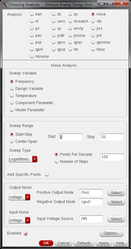
13 DC: Transient : AC: Noise: 13
: You can save the simulation setting as a state for the cellview Session => save state =>")
14 ADE window after entering all analyses above: - In the ADE window, select: simulation => options => analog. Enter the following settings to improve the accuracy of the simulation (compared to the default settings): You can save the simulation setting as a state for the cellview Session => save state => check the cellview option (and reopen it later with Session => load state => cellview option ): 14

15 - Notice the following menu in the ADE: Setup => simulator/directory/host => by default, the simulation data is stored in a subdirectory called simulation within your home directory. Within the simulation directory, the data is stored in subdirectories for each testbench. From time to time you might want to delete old simulation data to avoid reaching the data quota for your account (Simulations will abort in such a case.). For example, after finishing the work related to this testbench (AMPexample_TB), you can delete the data from a terminal window: # cd ~/simulation # ls [=> check that the AMPexample_TB folder is in this directory] # rm r AMPexample_TB When running long transient simulations, you can also save the data in the shared (public) temporary directory( /tmp ). To do so, go into the /tmp directory and use the mkdir command to create a subdirectory with your username. (Using your username as subdirectory will avoid that two users accidently use the same file names such as AMPexample_TB, which can cause Cadence to crash while running simulations.) Afterwards, change the project directory name to the newly created 15

16 directory as shown in the screenshot below. - Start the simulations by selection Simulation => Netlist and run from the ADE menu. - On ADE window, click Annotate => DC Operation Points. To see inside circuit of AMPexample, right click the AMPexample symbol and select Descend Read to open its schematic view. - One method to plot results is with the Cadence calculator (tools => calculator in the ADE window). For example, to plot the transient output, click on vt, click on the net labeled Out in the schematic, and then select Tools => plot from the calculator menu (as shown below) 16


17 Outputs can be added in the ADE (to be saved with states). In the ADE window, select Output => setup. Click on get expression, which will transfer the current formula in the calculator. => The transient output voltage will now be automatically plotted after a simulation. - One way to plot ac simulation results is with Results => Direct Plot => AC Gain & Phase in the ADE window. Then, select Out net in schematic window and the In net. Afterwards, press the ESC key. 17


18 - An alternative way for plotting results is with Results => direct plot => main form in the ADE window. Select the noise menu to plot noise as displayed below. Click on Plot. When Add to Outputs is selected, then the plot will also be saved in the ADE and automatically plotted after running another simulation. Use this window to plot input-referred noise and output-referred noise. 18

19 Results: - You can print noise summary in ADE with Results => Print => Noise Summary Select integrated noise range from lower 3dB frequency to upper 3dB frequency values from ac simulation. 19
")
20 ADE window after the simulation: (You can refresh the outputs with Results => Plot outputs => Expressions ) 20
21 4) Layout creation and verification a) Layout generation - Open the previously created AMPexample cellview from the library manager. - Select Launch => Layout XL from the menu => => => click ok, then yes at the next window 21


22 - The layout XL window below will be opened: - Select Connectivity => Generate => All from Source in the menu of the above layout window and use the following options: 22
 by changing Stop under Display Levels from 0 to 32: Also note in the above window that the X and Y Snap Spacing under Grid")
23 - Click shift + f to refresh the view and make all layers visible. Alternatively, you can update the displayed layers ( Options => Display ) by changing Stop under Display Levels from 0 to 32: Also note in the above window that the X and Y Snap Spacing under Grid Controls are set to You should not be able to see all components in the layout as below. Notice that the devices have the same dimensions (and parameter options) as in the schematic. 23


 on the drain. As can be seen in the screenshot below, the corresponding net in the schematic is highlighted to assist the routing.")
24 - Since the schematic window remains open (and linked) to the layout window when using Layout XL, you can select a device in the schematic and it will be heighted in the layout: - If you change device parameters in the schematic, you can use Connectivity => Update => Components and Nets in the layout window to automatically update the layout: - Zoom into the transistor (as below). Another Layout XL feature is that it highlights schematic elements to help manual routing when the path option is used. o Select metal 1 in the layer subwindow: o Use Create => Shape => path (shortcut: p ) in the main layout window to make a path. Click (left mouse button) on the drain. As can be seen in the screenshot below, the corresponding net in the schematic is highlighted to assist the routing. In addition, the line in the top right corner of the layout window leads to the next point where the drain should be connected in the layout. 24


25 o o Creating the path: move the mouse to stretch the path, left-click to make a corner, enter to end the path (at the other component to be connected). You can follow the other general Cadence tutorials on the Blackboard site for the course to complete the layout by moving and connecting components. The finished layout is displayed below as an example. Notice that it only serves for instructional purposes since it is not optimized according to the analog layout practices and recommendations discussed in the lecture/references. Some general and PDK-specific layout information and recommendations is included in the remainder of this subsection. - The capacitor connections have to be made on the metal 3 (top plate) and metal 2 (bottom plate) layers - To make connections between layers, you can use Create => Via. For example, to create vias between metals, one way is to use the single mode: 25


26 => creates a 2 x 2 via (2 rows and 2 columns) between metal 2 and metal 3. Alternatively, the stack mode can be used to place vias between multiple layers: => creates a 3 x 3 via stack between metal 1, 2, and 3 (connecting all of them) 26
 [To place contacts to N-wells (for connection to Vdd), you can use the M1_NWELL")
![option instead] - To place pins, select the appropriate pin layer in the layout window: (example Metal3_pin to place a pin on a](/docs-images/94/120060012/images/27-1.jpg "metal 3 area) Next, choose Create => Pin from the menu, and enter the following options: (example for VDD in the Terminal Name")
27 You can use the same menu to place a row or column of substrate contacts: => Creates a row of 10 contacts between the p-type substrate and metal 1 (to be connected to VSS) [To place contacts to N-wells (for connection to Vdd), you can use the M1_NWELL option instead] - To place pins, select the appropriate pin layer in the layout window: (example Metal3_pin to place a pin on a metal 3 area) Next, choose Create => Pin from the menu, and enter the following options: (example for VDD in the Terminal Name field) 27


28 You can now make a rectangle using the left mouse button in the layout, and finally place the label within the pin with another left-click: Note: All pin names in the layout and schematic must match exactly to pass LVS. 28


![named differenctly] # mkdir verification => When running verification tools, specify the verification directory with its full path in the Run Directory field (as in the relevant figures below).](/docs-images/94/120060012/images/29-2.jpg "You can click on to browse within your home directory. DRC (design rule check) In the layout window, select Assura => Run DRC.")
29 b) Layout verification Note, it is good practice to create a folder (example name: verification) within the subdirectory of the PDK folder. The data for DRC, LVS, and QRC should all be in the same folder, which can be ensured by specifying the correct path before running each tool (as shown in the run directory fields of the screenshots in this section). You can create a dedicated directory by entereing the following commands in a terminal window: # cd ~/cadence_gpdk180 [cadence_gpdk180 is the personal directory for the PDK, which you might have named differenctly] # mkdir verification => When running verification tools, specify the verification directory with its full path in the Run Directory field (as in the relevant figures below). You can click on to browse within your home directory. DRC (design rule check) In the layout window, select Assura => Run DRC. Specify the follwowing options, where the Run Directory should be the verification subdirectory within your home directory: You should receive a result without DRC errors: If some DRC rules are not satisified (see gpdk180_drm.pdf on the Blackboard site), then you will receive the following window: 29
![=> You can select the type of error (here [1] from the list), and lick](/docs-images/94/120060012/images/30-0.jpg "on the circled button to zoom into the next error occurance (the")


30 => You can select the type of error (here [1] from the list), and lick on the circled button to zoom into the next error occurance (the position and zoom in the layout window will be updated automatically). Fix all error an rerun the DRC until it is error-free. LVS (layout vs. schematic check) Select Assura => Run LVS in the layout window, and choose the same options as in the window below. The LVS result should be as follows: 30


31 If the layout and schematic have compenent or net mismatches, then you can use the following pop-up windows to find the errors: => => click on Open Tool => Resolve the problems and rerun LVS until the layout and schematic match. 31


32 Extraction (QRC) * Before executing extraction, make sure that you always complete the full DRC => LVS sequence. Even after small chagnes, you should run DRC and LVS before QRC. Select QRC => Setup QRC in the layout window. Go through the tabs and match all sections as shown in the screenshots below. 32

 should be")

33 Notes: - Use the default options for settigns that are not displayed above. - Extraction type: RC => With this option, parasitc resistances and capacitances will be extracted and added to the netlist for post-layout simulations - RefNode: VSS [The name of the ground pin in the schematic/layout (used for substrate biasing) should be specified as reference) - When done, click ok to finish the first setup step. As a second setup step, select Assura => Run QRC from the layout window, and match all settings as shown below. 33


34 - Click ok to run the QRC tool. The following message should be displayed afterward: 34


35 - Your library manager will now include an av_extracted cellview for the AMPexample cell: - Open the extracted cell view, click shift + f to display all layers, and zoom in to see parasitic resistors/capacitors that have been added: 35

 is modelled with six series segments of 22.")
36 - You can also check the values of the extracted devices. For example, after zooming into the top-left corner of the capacitor, you can use q to check its properties, including the value (912fF): - Notice that the resistor (schematic: 195Ω / 6 segments = 32.5Ω per segment) is modelled with six series segments of 22.5Ω (poly) and 10Ω (interconnect) resistances in the extraced cellview. 36


37 5) Post-layout simulation a) Configuration file setup - In the library manager, highlight the testbench for the circuit (e.g., AMPexample_TB) as shown below and create a configuration file ( File => New => Cellview). - Select the appropriate options in the following sequence of windows: => (The second window initially contains only blank fields. Click on Use Template and then select spectre to automatically populate the fields as shown above. Then, change the View [under TopCell] to schematic.) 37


38 - The following window should appear: Note: After creating and editing new cells, you should always update the config file using the button circled above. - Click File => save. - Right-click on the schematic field of the AMPexample cell, and select the av_extracted view: 38


39 - The window should now appear as below. Now, the av_extracted cellview will be used for the AMPexample cell when the AMPexample_TB schematic is simulated. Thus, the effect of the extracted layout parasitics will become evident in the simulation results. Save the config file and close it. - The config file view can be found in the library manager. Select it, and then choose File => open with the options displayed below, which will open the config and schematic window. 39


40 - In the schematic cellview (AMPexample_TB), notice that when you select the AMPexample cell, and use Edit => Hierarchy => Descend Edit; then the av_extracted cellview will appear as default in the top of the list: If you want to, you can descend into the extracted view and later return with Edit => Hierarchy => Return b) Running the post-layout simulation - From the AMPexample_TB schematic, select Launch => ADE L. - From the ADE menu, load the previously saved state ( Session => load state => cellview tab ): 40

![You can use the /tmp/[your_account] directory to avoid that.) - Check your plots and saved outputs.](/docs-images/94/120060012/images/41-2.jpg "Notice that the results with the av_extracted view (below) are different compared to the previous results from simulation of the schematic view.")
41 - Start the post-layout simulation with Simulation => Netlist and Run o When running post-layout simulations, you can also save the data in the temporary directory: - in ADE: Setup => simulator/directory/host (If your disk quota in the simulation directory within your home directory exceeds the limit, then Cadence might crash. You can use the /tmp/[your_account] directory to avoid that.) - Check your plots and saved outputs. Notice that the results with the av_extracted view (below) are different compared to the previous results from simulation of the schematic view. If the post-layout simulation performance degradation is not acceptable, then layout has to be optimized. - Note: You can use the config file to switch back to a simulation using the schematic cellview of AMPexample. To do so, simple change (right-click on av_extracted view) to the schematic view in the config file and save it afterwards: 41
Cadence IC Design Manual
 Cadence IC Design Manual For EE5518 ZHENG Huan Qun Lin Long Yang Revised on May 2017 Department of Electrical & Computer Engineering National University of Singapore 1 P age Contents 1 INTRODUCTION...
Professor Muller Fall 2016 Sameet Ramakrishnan Eric Chang Adapted from prior EE140 and EE141 labs. EE 140/240A Lab 0 Full IC Design Flow
 Professor Muller Fall 2016 Sameet Ramakrishnan Eric Chang Adapted from prior EE140 and EE141 labs EE 140/240A Lab 0 Full IC Design Flow In this lab, you will walk through the full process an analog designer
Creating the inv1 cell WITHOUT power pins
 Simulating with extracted parasitic Let s assume I designed the cell inv1, for which I created the views schematic, symbol and layout. Creating the inv1 cell WITHOUT power pins First, create the inverter
Virtuoso Layout Editor
 This tutorial will cover the basic steps involved in using the Cadence layout editor called Virtuoso, extracting layout, and running simulation on the layout. The inverter layout is used as an example
TUTORIAL II ECE 555 / 755 Updated on September 11 th 2006 CADENCE LAYOUT AND PARASITIC EXTRACTION
 TUTORIAL II ECE 555 / 755 Updated on September 11 th 2006 CADENCE LAYOUT AND PARASITIC EXTRACTION After finishing a schematic of your design (Tutorial-I), the next step is creating masks which are for
ECE471/571 Energy Efficient VLSI Design Project 2 Cadence Setup and Creation of an Inverter Due Date 11:30 am on Friday, February 2 nd, 2018
 ECE471/571 Energy Efficient VLSI Design Project 2 Cadence Setup and Creation of an Inverter Due Date 11:30 am on Friday, February 2 nd, 2018 Introduction This project will first walk you through the setup
Lab 2. Standard Cell layout.
 Lab 2. Standard Cell layout. The purpose of this lab is to demonstrate CMOS-standard cell design. Use the lab instructions and the cadence manual (http://www.es.lth.se/ugradcourses/cadsys/cadence.html)
CPE/EE 427, CPE 527, VLSI Design I: Tutorial #2, Schematic Capture, DC Analysis, Transient Analysis (Inverter, NAND2)
") CPE/EE 427, CPE 527, VLSI Design I: Tutorial #2, Schematic Capture, DC Analysis, Transient Analysis (Inverter, NAND2) Joel Wilder, Aleksandar Milenkovic, ECE Dept., The University of Alabama in Huntsville
CPE/EE 427, CPE 527, VLSI Design I: Tutorial #2, Schematic Capture, DC Analysis, Transient Analysis (Inverter, NAND2) Joel Wilder, Aleksandar Milenkovic, ECE Dept., The University of Alabama in Huntsville
UNIVERSITY OF WATERLOO
 UNIVERSITY OF WATERLOO UW ASIC DESIGN TEAM: Cadence Tutorial Description: Part I: Layout & DRC of a CMOS inverter. Part II: Extraction & LVS of a CMOS inverter. Part III: Post-Layout Simulation. The Cadence
ANALOG MICROELECTRONICS ( A)
") ANALOG MICROELECTRONICS (304-534A) IBM 130 nm CMOS Technology An Introduction to Cadence Virtuoso Layout Tool and the Analog Simulation Environment Prepared By - Azhar A. Chowdhury Updated by Ming Yang
ANALOG MICROELECTRONICS (304-534A) IBM 130 nm CMOS Technology An Introduction to Cadence Virtuoso Layout Tool and the Analog Simulation Environment Prepared By - Azhar A. Chowdhury Updated by Ming Yang
Cadence Virtuoso Schematic Design and Circuit Simulation Tutorial
 Cadence Virtuoso Schematic Design and Circuit Simulation Tutorial Introduction This tutorial is an introduction to schematic capture and circuit simulation for ENGN1600 using Cadence Virtuoso. These courses
Cadence Tutorial. Introduction to Cadence 0.18um, Implementation and Simulation of an inverter. A. Moradi, A. Miled et M. Sawan
 Cadence Tutorial Introduction to Cadence 0.18um, Implementation and Simulation of an inverter A. Moradi, A. Miled et M. Sawan Section 1: Introduction to Cadence You will see how to create a new library
Cadence Tutorial A: Schematic Entry and Functional Simulation Created for the MSU VLSI program by Andrew Mason and the AMSaC lab group.
 Cadence Tutorial A: Schematic Entry and Functional Simulation Created for the MSU VLSI program by Andrew Mason and the AMSaC lab group. Revision Notes: Aug. 2003 update and edit A. Mason add intro/revision/contents
EE 330 Spring 2018 Laboratory 2: Basic Boolean Circuits
 EE 330 Spring 2018 Laboratory 2: Basic Boolean Circuits Contents Objective:... 2 Part 1: Introduction... 2 Part 2 Simulation of a CMOS Inverter... 3 Part 2.1 Attaching technology information... 3 Part
EE115C Digital Electronic Circuits. Tutorial 4: Schematic-driven Layout (Virtuoso XL)
") EE115C Digital Electronic Circuits Tutorial 4: Schematic-driven Layout (Virtuoso XL) This tutorial will demonstrate schematic-driven layout on the example of a 2-input NAND gate. Simple Layout (that won
EE115C Digital Electronic Circuits Tutorial 4: Schematic-driven Layout (Virtuoso XL) This tutorial will demonstrate schematic-driven layout on the example of a 2-input NAND gate. Simple Layout (that won
S Exercise 1C Testing the Ring Oscillator
 S-87.3148 Exercise 1C Testing the Ring Oscillator Aalto University School of Electrical Engineering Department of Micro- and Nanosciences (ECDL) 10.9.2014 1 1 Building the test bench In this exercise,
Revision Notes: July2004 Generate tutorial for single transistor analysis. Based on existing schematic entry tutorial developed for ECE410
 Cadence Analog Tutorial 1: Schematic Entry and Transistor Characterization Created for the MSU VLSI program by Professor A. Mason and the AMSaC lab group. Revision Notes: July2004 Generate tutorial for
Design rule illustrations for the AMI C5N process can be found at:
 Cadence Tutorial B: Layout, DRC, Extraction, and LVS Created for the MSU VLSI program by Professor A. Mason and the AMSaC lab group. Revised by C Young & Waqar A Qureshi -FS08 Document Contents Introduction
Virtuoso Schematic Composer
 is a schematic design tool from Cadence. In this tutorial you will learn how to put electrical components, make wire connections, insert pins and check for connection error. Start Cadence Custom IC Design
VLSI Lab Tutorial 3. Virtuoso Layout Editing Introduction
 VLSI Lab Tutorial 3 Virtuoso Layout Editing Introduction 1.0 Introduction The purpose of this lab tutorial is to guide you through the design process in creating a custom IC layout for your CMOS inverter
Cadence Tutorial 2: Layout, DRC/LVS and Circuit Simulation with Extracted Parasitics
 Cadence Tutorial 2: Layout, DRC/LVS and Circuit Simulation with Extracted Parasitics Introduction This tutorial describes how to generate a mask layout in the Cadence Virtuoso Layout Editor. Use of DIVA
EECE 285 VLSI Design. Cadence Tutorial EECE 285 VLSI. By: Kevin Dick Co-author: Jeff Kauppila Co-author: Dr. Arthur Witulski
 Cadence Tutorial EECE 285 VLSI By: Kevin Dick Co-author: Jeff Kauppila Co-author: Dr. Arthur Witulski 1 Table of Contents Purpose of Cadence 1) The Purpose of Cadence pg. 4 Linux 1) The Purpose of Linux
FACULTY OF ENGINEERING MULTIMEDIA UNIVERSITY LAB SHEET DIGITAL INTEGRATED CIRCUIT
 FACULTY OF ENGINEERING MULTIMEDIA UNIVERSITY LAB SHEET DIGITAL INTEGRATED CIRCUIT DIC1: Schematic Design Entry, Simulation & Verification DIC2: Schematic Driven Layout Drawing (SDL) Design Rule Check (DRC)
Cadence Schematic Tutorial. EEE5320/EEE4306 Fall 2015 University of Florida ECE
 Cadence Schematic Tutorial EEE5320/EEE4306 Fall 2015 University of Florida ECE 1 Remote access You may access the Linux server directly from the NEB Computer Lab using your GatorLink username and password.
Cadence Tutorial A: Schematic Entry and Functional Simulation Created for the MSU VLSI program by Professor A. Mason and the AMSaC lab group.
 Cadence Tutorial A: Schematic Entry and Functional Simulation Created for the MSU VLSI program by Professor A. Mason and the AMSaC lab group. Revision Notes: Jan. 2006 Updated for use with spectre simulator
Logging in, starting a shell tool, and starting the Cadence Tool Suite
 EEE 4134 VLSI I Laboratory Lab 0 (Introductory Lab) Logging into Cadence Server, Tool Setup, Cell Library Creation, Introduction to Custom IC Design flow Objectives: To login, start a shell tool and start
CADENCE SETUP. ECE4430-Analog IC Design
 CADENCE SETUP This short tutorial shows how to configure Cadence to use the NCSU Cadence Design Kit (CDK) with access to the ON Semiconductor C5 0.5-µm and the TSMC 0.35-µm CMOS processes libraries. In
Microelectronica. Full-Custom Design with Cadence Tutorial
 Área Científica de Electrónica Microelectronica Full-Custom Design with Cadence Tutorial AustriaMicroSystems C35B3 (HIT-Kit 3.70) Marcelino Santos Table of contends 1. Starting Cadence... 3 Starting Cadence
EE 330 Laboratory 3 Layout, DRC, and LVS Fall 2015
 EE 330 Laboratory 3 Layout, DRC, and LVS Fall 2015 Contents Objective:... 2 Part 1 Creating a layout... 2 1.1 Run DRC Early and Often... 2 1.2 Create N active and connect the transistors... 3 1.3 Vias...
Cadence Tutorial: Schematic Entry and Circuit Simulation of a CMOS Inverter
 Cadence Tutorial: Schematic Entry and Circuit Simulation of a CMOS Inverter Introduction This tutorial describes the steps involved in the design and simulation of a CMOS inverter using the Cadence Virtuoso
Lab 1: An Introduction to Cadence
 GIF-4201/GEL-7016 (Micro-électronique) Lab 1: An Introduction to Cadence Schematic, simulation and layout Gabriel Gagnon-Turcotte, Mehdi Noormohammadi Khiarak and Benoit Gosselin Department of Electrical
EE 140/240A - Full IC Design Flow Tutorial
 Original document by Filip Maksimovic & Mike Lorek, Spring 2015, derived from earlier EE141 lab manuals Revisions for IC6 by David Burnett & Thaibao Phan, Spring 2016 Revisions made by Nandish Mehta to
Using Cadence Virtuoso, a UNIX based OrCAD PSpice like program, Remotely on a Windows Machine
 Using Cadence Virtuoso, a UNIX based OrCAD PSpice like program, Remotely on a Windows Machine A. Launch PuTTY. 1. Load the Saved Session that has Enable X11 forwarding and the Host Name is cvl.ece.vt.edu.
More information can be found in the Cadence manuals Virtuoso Layout Editor User Guide and Cadence Hierarchy Editor User Guide.
 Chapter 6 Building with Layout This chapter consists of two parts. The first describes the generation of layout views and the second deals with the various tools used for verifying the layout, both physical
EE4111 Advanced Analog Electronics Design. Spring 2009 Experiment #4 April 6 ~ April 17
 EE4111 Advanced Analog Electronics Design Spring 2009 Experiment #4 April 6 ~ April 17 Setup Cadence in VLSI Lab 1) Copy files $ cp r /home/grads/ee4111ta ~/ 2) Edit your.cshrc file -- Include the following
AMS 0.18 µm PDK Setup and Cadence Tutorial Contributors
 AMS 0.18 µm PDK Setup and Cadence Tutorial Contributors Muhammad Ahmed, Sita Asar, and Ayman Fayed, Power Management Research Lab, https://pmrl.osu.edu, Department of Electrical and Computer Engineering,
ECE471/571 Energy Ecient VLSI Design
 ECE471/571 Energy Ecient VLSI Design Project 2 Cadence Setup and Creation of an Inverter Due Date 11:30pm on Friday, January 30 th 2015 Introduction This project will rst walk you through the setup for
Process technology and introduction to physical
 Neuromorphic Engineering II Lab 3, Spring 2014 1 Lab 3 March 10, 2014 Process technology and introduction to physical layout Today you will start to learn to use the Virtuoso layout editor XL which is
EE434 ASIC & Digital Systems. From Layout to SPICE Simulation (Virtuoso, Calibre, HSpice) Spring 2017 Dae Hyun Kim
 Spring 2017 Dae Hyun Kim") EE434 ASIC & Digital Systems From Layout to SPICE Simulation (Virtuoso, Calibre, HSpice) Spring 2017 Dae Hyun Kim daehyun@eecs.wsu.edu 1 Preparation for Lab2 Download the following file into your working
EE434 ASIC & Digital Systems From Layout to SPICE Simulation (Virtuoso, Calibre, HSpice) Spring 2017 Dae Hyun Kim daehyun@eecs.wsu.edu 1 Preparation for Lab2 Download the following file into your working
CS755 CAD TOOL TUTORIAL
 CS755 CAD TOOL TUTORIAL CREATING SCHEMATIC IN CADENCE Shi-Ting Zhou shi-ting@cs.wisc.edu After you have figured out what you want to design, and drafted some pictures and diagrams, it s time to input schematics
Tutorial on getting started in Cadence. Advanced Analog Circuits Spring 2015 Instructor: Prof. Harish Krishnaswamy TA: Jahnavi Sharma
 Tutorial on getting started in Cadence Advanced Analog Circuits Spring 2015 Instructor: Prof. Harish Krishnaswamy TA: Jahnavi Sharma Getting Started Start Cadence from the terminal by using the command
EE 330 Laboratory 3 Layout, DRC, and LVS
 EE 330 Laboratory 3 Layout, DRC, and LVS Spring 2018 Contents Objective:... 2 Part 1 creating a layout... 2 1.1 Run DRC... 2 1.2 Stick Diagram to Physical Layer... 3 1.3 Bulk Connections... 3 1.4 Pins...
EDA-BASED DESIGN PRACTICAL LABORATORY SESSION No. 3
 LABORATOIRE DE SYSTEMES MICROELECTRONIQUES EPFL STI IMM LSM ELD Station nº 11 CH-1015 Lausanne Téléphone : Fax : E-mail : Site web : +4121 693 6955 +4121 693 6959 lsm@epfl.ch lsm.epfl.ch EDA-BASED DESIGN
EE115C Digital Electronic Circuits. Tutorial 2: Hierarchical Schematic and Simulation
 EE115C Digital Electronic Circuits Tutorial 2: Hierarchical Schematic and Simulation The objectives are to become familiar with Virtuoso schematic editor, learn how to create the symbol view of basic primitives,
ESE 570 Cadence Lab Assignment 2: Introduction to Spectre, Manual Layout Drawing and Post Layout Simulation (PLS)
") ESE 570 Cadence Lab Assignment 2: Introduction to Spectre, Manual Layout Drawing and Post Layout Simulation (PLS) Objective Part A: To become acquainted with Spectre (or HSpice) by simulating an inverter,
ESE 570 Cadence Lab Assignment 2: Introduction to Spectre, Manual Layout Drawing and Post Layout Simulation (PLS) Objective Part A: To become acquainted with Spectre (or HSpice) by simulating an inverter,
Lab 1: Cadence Custom IC design tools- Setup, Schematic capture and simulation
 Lab 1: Cadence Custom IC design tools- Setup, Schematic capture and simulation Brittany Duffy EE 330- Integrated Electronics Lab Section B Professor Randy Geiger 1/24/13 Introduction The main goal of this
Cadence Tutorial C: Simulating DC and Timing Characteristics 1
 Cadence Tutorial C: Simulating DC and Timing Characteristics Created for the MSU VLSI program by Professor A. Mason and the AMSaC lab group Last updated by Patrick O Hara SS15 Document Contents Introduction
CPE/EE 427, CPE 527, VLSI Design I: Tutorial #1, Full Custom VLSI (inverter layout)
") CPE/EE 427, CPE 527, VLSI Design I: Tutorial #1, Full Custom VLSI (inverter layout) Joel Wilder, Aleksandar Milenkovic, ECE Dept., The University of Alabama in Huntsville Adapted from Virginia Tech, Dept.
CPE/EE 427, CPE 527, VLSI Design I: Tutorial #1, Full Custom VLSI (inverter layout) Joel Wilder, Aleksandar Milenkovic, ECE Dept., The University of Alabama in Huntsville Adapted from Virginia Tech, Dept.
CMOS Design Lab Manual
 CMOS Design Lab Manual Developed By University Program Team CoreEl Technologies (I) Pvt. Ltd. 1 Objective Objective of this lab is to learn the Mentor Graphics HEP2 tools as well learn the flow of the
Cadence Virtuoso Simulation of a pixel
 MEMS AND MICROSENSORS 2018/2019 Cadence Virtuoso Simulation of a pixel 11/12/2018 Giorgio Mussi giorgio.mussi@polimi.it Introduction In this lab, we will use Cadence Virtuoso to simulate a sub-array of
Experiment 0: Introduction to Cadence
 UNIVERSITY OF CALIFORNIA AT BERKELEY College of Engineering Department of Electrical Engineering and Computer Sciences EE105 Lab Experiments Experiment 0: Introduction to Cadence Contents 1. Introduction...
Prepared by Dr. Ulkuhan Guler GT-Bionics Lab Georgia Institute of Technology
 Prepared by Dr. Ulkuhan Guler GT-Bionics Lab Georgia Institute of Technology OUTLINE Introduction Mapping for Schematic and Layout Connectivity Generate Layout from Schematic Connectivity Some Useful Features
DOWNLOAD PDF CADENCE WAVEFORM CALCULATOR USER GUIDE
 Chapter 1 : CSE / Cadence Tutorial The Cadence Design Communities support Cadence users and technologists interacting to exchange ideas, news, technical information, and best practices to solve problems
CS/EE 5720/6720 Analog IC Design Tutorial for Schematic Design and Analysis using Spectre
 CS/EE 5720/6720 Analog IC Design Tutorial for Schematic Design and Analysis using Spectre Introduction to Cadence EDA: The Cadence toolset is a complete microchip EDA (Electronic Design Automation) system,
EE 330 Spring Laboratory 2: Basic Boolean Circuits
 EE 330 Spring 2013 Laboratory 2: Basic Boolean Circuits Objective: The objective of this experiment is to investigate methods for evaluating the performance of Boolean circuits. Emphasis will be placed
Cadence Analog Circuit Tutorial
 Cadence Analog Circuit Tutorial Schematic Entry for Analog Designs- Passive Circuits (RLC Circuit) In this tutorial, we will build the circuit shown in figure 1 below, using the Cadence Composer tool.
VLSI Lab Tutorial 1. Cadence Virtuoso Schematic Composer Introduction
 VLSI Lab Tutorial 1 Cadence Virtuoso Schematic Composer Introduction 1.0 Introduction The purpose of the first lab tutorial is to help you become familiar with the schematic editor, Virtuoso Schematic
UNIVERSITY OF CALIFORNIA College of Engineering Department of Electrical Engineering and Computer Sciences Lab #2: Layout and Simulation
 UNIVERSITY OF CALIFORNIA College of Engineering Department of Electrical Engineering and Computer Sciences Lab #2: Layout and Simulation NTU IC541CA 1 Assumed Knowledge This lab assumes use of the Electric
ESE570 Spring University of Pennsylvania Department of Electrical and System Engineering Digital Integrated Cicruits AND VLSI Fundamentals
 University of Pennsylvania Department of Electrical and System Engineering Digital Integrated Cicruits AND VLSI Fundamentals ESE570, Spring 2019 HW5: Delay and Layout Sunday, February 17th Due: Friday,
Guide to the CSE 577 Lab and Cad tools
 Guide to the CSE 577 Lab and Cad tools 1. Introduction The objective of this tutorial is to give you an overview to (1) setup the Cadence and Synopsys hspice tools for your account in IST 218 Lab, (2)
ECE 331: Electronics Principles I Fall 2014
 ECE 331: Electronics Principles I Fall 2014 Lab #0: Introduction to Computer Modeling and Laboratory Measurements Report due at your registered lab period on the week of Sept. 8-12 Week 1 Accessing Linux
Cadence Tutorial D: Using Design Variables and Parametric Analysis Document Contents Introduction Using Design Variables Apply Apply
 Cadence Tutorial D: Using Design Variables and Parametric Analysis Created for the MSU VLSI program by Casey Wallace Last Updated by: Patrick O Hara SS15 Document Contents Introduction Using Design Variables
Verifying the Multiplexer Layout
 4 This chapter introduces you to interactive verification. You will perform two different tests in the Virtuoso layout editor while using Assura interactive verification products. One test uses the Design
DRC and LVS checks using Cadence Virtuoso Version 3.0
 DRC and LVS checks using Cadence Virtuoso Version 3.0 Start virtuoso l l Open a virtuoso session in the directory which contains the required cds.lib and lib.def files. Command : virtuoso & Open the layout
Fall 2008: EE5323 VLSI Design I using Cadence
 1 of 23 9/17/2008 6:47 PM Fall 2008: EE5323 VLSI Design I using Cadence This tutorial has been adapted from EE5323 offered in Fall 2007. Thanks to Jie Gu, Prof. Chris Kim and Satish Sivaswamy of the University
This is a brief tutorial about building a Symbol for a Schematic in Cadence IC design tool environment for hierarchical design of schematics.
 This is a brief tutorial about building a Symbol for a Schematic in Cadence IC design tool environment for hierarchical design of schematics. 1. > cd work035 2. > cadsetup ams035 3. > virtuoso& IMPORTANT:
Intro to Cadence. Brady Salz. ECE483 Spring 17
 Intro to Cadence Brady Salz ECE483 Spring 17 What We re Doing Learn you a Cadence Learn simulation vocabulary Basic schematic guidelines Simulation results Init Before we begin, open a terminal: $ module
Laboratory 3. EE 342 (VLSI Circuit Design) - Using Spectre netlist and Calculator for simulation
 - Using Spectre netlist and Calculator for simulation") EE 342 (VLSI Circuit Design) Laboratory 3 - Using Spectre netlist and Calculator for simulation By Mulong Li, 2013 1 Background knowledge Spectre: is a SPICE-class circuit simulator. It provides the basic
EE 342 (VLSI Circuit Design) Laboratory 3 - Using Spectre netlist and Calculator for simulation By Mulong Li, 2013 1 Background knowledge Spectre: is a SPICE-class circuit simulator. It provides the basic
The original document link is
 Tutorial:Analog Artist with HSPICE The original document link is http://www.eda.ncsu.edu/wiki/tutorial:analog_artist_with_hspice This tutorial will introduce you to the Cadence Environment: specifically
Introduction to laboratory exercises in Digital IC Design.
 Introduction to laboratory exercises in Digital IC Design. A digital ASIC typically consists of four parts: Controller, datapath, memory, and I/O. The digital ASIC below, which is an FFT/IFFT co-processor,
Basic Analog Simulation in Cadence
 York University Department of Electrical Engineering and Computer Science EMIL Tutorial Series Tutorial #1 Basic Analog Simulation in Cadence In this tutorial we step through how to start Cadence (or at
Click on the SwCAD III shortcut created by the software installation.
 LTSpice Guide Click on the SwCAD III shortcut created by the software installation. Select File and New Schematic. Add a component Add a resistor Press R or click the resistor button to insert a resistor.
Full Custom Integrated Circuit (IC) Design Flow at U.S. Army Research Laboratory
 Design Flow at U.S. Army Research Laboratory") Full Custom Integrated Circuit (IC) Design Flow at U.S. Army Research Laboratory by James Wilson ARL-TN-0422 February 2011 Approved for public release; distribution unlimited. NOTICES Disclaimers The findings
Full Custom Integrated Circuit (IC) Design Flow at U.S. Army Research Laboratory by James Wilson ARL-TN-0422 February 2011 Approved for public release; distribution unlimited. NOTICES Disclaimers The findings
DC Circuit Simulation
 Chapter 2 DC Circuit Simulation 2.1 Starting the Project Manager 1. Select Project Manager from the Start All Program Cadence Release 16.5 Project Manager. 2. Select Allegro PCB Designer (Schematic) from
EE5323/5324 VLSI Design I/II using Cadence
 1 of 18 2009-1-23 23:58 Spring 2009: EE5323/5324 VLSI Design I/II using Cadence This tutorial has been adapted from EE5323 offered in Fall 2007. Thanks to Jie Gu, Prof. Chris Kim and Satish Sivaswamy of
HOMEWORK 9 CMPEN 411 Due: 4/12/ :30pm
 HOMEWORK 9 CMPEN 411 Due: 4/12/2016 11:30pm Learning Objective Complete the full 8 bit RISC microprocessor chip design by placing the processor core design into the 40 pin 'tiny' chip pad frame. Do verify
RC Extraction. of an Inverter Circuit
 RC Extraction of an Inverter Circuit Santa Clara University Department of Electrical Engineering Under Guidance of Dr Samiha Mourad & Dr Shoba Krishnan Date of Last Revision: February 1, 2010 Copyright
Select the technology library: NCSU_TechLib_ami06, then press OK.
 ECE 126 Inverter Tutorial: Schematic & Symbol Creation Created for GWU by Anis Nurashikin Nordin & Thomas Farmer Tutorial adapted from: http://www.ee.ttu.edu/ee/cadence/commondirectory/final%20tutorials/digitalcircuitsimulationusingvirtuoso.doc
TQPED MMIC Design Training
 TQPED MMIC Design Training Outline Installation and Use of the Library AWR AWR Design Kit (PDK Process Design Kit) ICED Layout Kit Create a new document using the Library Environment Setup Hotkeys Background
HOMEWORK 10 CMPEN 411 Due: 4/28/ :30pm
 HOMEWORK 10 CMPEN 411 Due: 4/28/2016 11:30pm Instruction First, fabrication ready the full 8 bit RISC microprocessor chip: redesign the chip (its components) to fit the entire chip fitted into the 40 pin
Analog IC Schematic Capture. Mentor Graphics 2006
 Analog IC Schematic Capture Mentor Graphics 2006 Santa Clara University Department of Electrical Engineering Date of Last Revision: February 6, 2007 Table of Contents 1. Objective...3 2. Setup & Preparation...4
DRC and LVS checks using Cadence Virtuoso Version 2.0
 DRC and LVS checks using Cadence Virtuoso Version 2.0 Start virtuoso l l Open a virtuoso session in the directory which contains the required cds.lib and lib.def files. Command : virtuoso & Open the layout
Lab 4 LVS and Post layout Simulation
 Lab 4 LVS and Post layout Simulation Objective: In this lab you will learn 1. How to check if your layout that you drew in lab 3 matches your schematic that you drew in lab 2. 2. How to do the post layout
EEC 116 Fall 2011 Lab #1 Cadence Schematic Capture and Layout Tutorial
 EEC 116 Fall 2011 Lab #1 Cadence Schematic Capture and Layout Tutorial Dept. of Electrical and Computer Engineering University of California, Davis September 26, 2011 Reading: Rabaey Chapters 1, 2, A,
MENTOR GRAPHICS IC DESIGN MANUAL. Schematic & Simulation. Gun Jun K Praveen Jayakar Thomas Zheng Huan Qun
 MENTOR GRAPHICS IC DESIGN MANUAL Schematic & Simulation By Gun Jun K Praveen Jayakar Thomas Zheng Huan Qun August 2004 Signal Processing & VLSI Design Laboratory Department of Electrical & Computer Engineering
Introduction to Design Architect
 SANTA CLARA UNIVERSITY Dept. of Electrical Engineering Mentor Graphics Tutorials Introduction to Design Architect Yiching Chen Sangeetha Raman S. Krishnan I. Introduction II. This document contains a step-by-step
A Tutorial on Using the Cadence Virtuoso Editor to create a CMOS Inverter with CMOSIS5 Technology
 A Tutorial on Using the Cadence Virtuoso Editor to create a CMOS Inverter with CMOSIS Technology Developed by Ted Obuchowicz VLSI/CAD Specialist, Dept. of Electrical and Computer Engineering Concordia
Layout and Layout Verification. of an Inverter Circuit
 Layout and Layout Verification of an Inverter Circuit Santa Clara University Department of Electrical Engineering By Piyush Panwar Under Guidance of Dr Samiha Mourad Date of Last Revision: August 7, 2010
Mentor Graphics VLSI CAD Tutorials
 VLSI Design Flow Using Mentor-Graphics Tools Mentor Graphics VLSI CAD Tutorials School of Engineering Santa Clara University Santa Clara, CA 95053 At the Design Center, School of Engineering, of Santa
Place & Route: Using Silicon Ensemble
 Place & Route: Using Silicon Ensemble Introduction In a typical digital design flow, hardware description language is used to model a design and verify desired behavior. Once the desired functionality
Introduction to CCV and Cadence Virtuoso for Electronic Circuit Simulation
 Introduction to CCV and Cadence Virtuoso for Electronic Circuit Simulation Introduction ENGN1600 will be using the Cadence Virtuoso software suite for its circuit design and SPICE components. Part of the
Lesson 9: Processing a Schematic Design
 Lesson 9: Processing a Schematic Design Lesson Objectives After you complete this lab you will be able to: Assign reference designators Check the design for errors Create a netlist for OrCAD and Allegro
OPUS -- AMS 3.2. Version Manual
 OPUS -- AMS 3.2 Version 4.4.3 Manual for students designing VLSI integrated circuits at the VLSI laboratory of the DED (V2-324) using the OPUS Design Environment on Sun workstations under the UNIX Operating
Mixed Signal Design Simulation Manual
 CADENCE Mixed Signal Design Simulation Manual Version 1.0 By Zheng Huan Qun February 2005 Department of Electrical and Computer Engineering National University of Singapore ACKNOWLEDGMENTS The author would
Copyright 2008 Linear Technology. All rights reserved. Getting Started
 Copyright. All rights reserved. Getting Started Copyright. All rights reserved. Draft a Design Using the Schematic Editor 14 Start with a New Schematic New Schematic Left click on the New Schematic symbol
ECEN 474 Homework #2 Notes
 ECEN 474 Homework #2 Notes February 22, 2018 Due: 3-6-2018, 5:00PM Homeworks will not be received after due. Instructor: Sam Palermo 1. (50 points) Technology Characterization for Design In this problem,
ELEC451 Integrated Circuit Engineering Using Cadence's Virtuoso Layout Editing Tool
 ELEC451 Integrated Circuit Engineering Using Cadence's Virtuoso Layout Editing Tool Contents Contents 1. General 2. Creating and Working On a Layout o 2.1 Undoing/Re-doing an Action o 2.2 Display Options
EE 210 Lab Assignment #2: Intro to PSPICE
 EE 210 Lab Assignment #2: Intro to PSPICE ITEMS REQUIRED None Non-formal Report due at the ASSIGNMENT beginning of the next lab no conclusion required Answers and results from all of the numbered, bolded
Using Sonnet in a Cadence Virtuoso Design Flow
 Using Sonnet in a Cadence Virtuoso Design Flow Purpose of this document: This document describes the Sonnet plug-in integration for the Cadence Virtuoso design flow, for silicon accurate EM modelling of
OrCad & Spice Tutorial By, Ronak Gandhi Syracuse University
 OrCad & Spice Tutorial By, Ronak Gandhi Syracuse University Brief overview: OrCad is a suite of tools from Cadence for the design and layout of circuit design and PCB design. We are currently using version