session 7. Datapath Design
|
|
|
- Pauline Terry
- 6 years ago
- Views:
Transcription
1 General Objective: Determine the hardware requirement of a digital computer based on its instruction set. Specific Objectives: Describe the general concepts in designing the data path of a digital computer from its instruction set. Design the data processing elements such as the arithmetic circuits, counters and registers. Design data routing circuits that transport data to various processing elements. Draw the interconnections of the various elements. 1
2 General concepts in designing the data path of a digital computer from its instruction set. Instruction Set Mnemonic OpCode LDA ADD 1 SUB 1 OUT HLT Description Load ACC with the contents of the memory specified address. Add the contents of the ACC with the contents of the B register and place the result in the ACC. SUBtract the contents of the B register from the ACC and store the result in the ACC. OUTput he contents of the ACC to the OUTR register. Halt or stop MSAP. Instruction Format D7 D6 D5 D4 OPCODE D3 D2 D1 D OPERAND 2
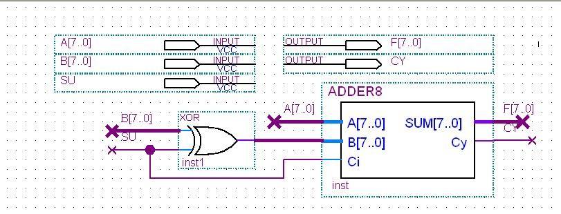
3 Extracting hardware requirements from the Instruction Set 1. Starting with the arithmetic instructions, ADD and SUB, ADD M[address] and SUB M[address] which mean add (subtract) the contents of the memory specified in the instruction from the contents of the accumulator and store the results to the accumulator. Symbolically, ACC <= ACC + M[address] or ACC <= ACC - M[address] one addend (minuend) is already in the ACC, while the other addend (subtrahend is found in the memory. It is typical that the data read from the memory is stored in a temporary register. This will lead to a configuration below; ACC ACC + TMP TMP 3
4 combining the add and subtract operations, ACC +/TMP su The addition or subtraction operation is selected by su. When su =, add operation is performed. when su = 1, subtraction is performed. 4
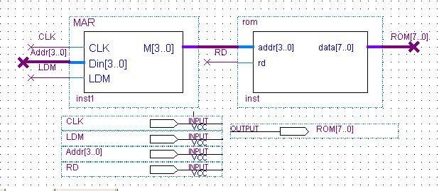
5 2. Memory Operation. Data manipulated by the arithmetic operations are stored in the memory. Accessing the memory requires two signals; the address signal which specifies the location of the data in the memory, and the rd control signal which specifies the exact time data is outputted by the memory. The address must be constantly applied to the memory during the entire memory read cycle. This necessitates the use of a register to hold the address, thus it is named the Memory Address Register (MAR).The size of MAR is equal to the number of address bits. Symbolically, memory read operation is represented as, rd : REG <= M[MAR] Memory Unit (2N x M MAR N Address Data out M REG rd 5
6 3. Sequencing of memory access. The memory contains both sequences of instruction codes (computer program), and operands (data to be manipulated by the program). The instruction code must be first read (fetched) from memory, decoded, and the memory is read again to get the operand (operand fetch). Processing of data then can be carried out (executed), in the processing elements. The type of processing ( arithmetic) is indicated by the instruction code. Thus, the computer cycles between operation code and operand fetch cycle (opcode and operand fetch), and the execute cycle. To keep track of the instruction code to be fetched next from memory, a Program Counter (PC) is used to always point to a memory address containing the next instruction code to be fetched. PC Memory Unit (2N x M) opcode/ operand fetch cycle EXecute Cycle MAR N Address Data out M rd 6
7 4. Fetch Cycle and Operand Fetch During the OpCode Fetch, the instruction code is read from memory and then stored in a special register called as the Instruction Register (IR). During the operand fetch, the address of the operand is stored in MAR in preparation to read the data from memory. Generally, data read from memory during operand fetch is stored in a general purpose register (example, the ACCumulator register). PC PC Memory Unit (2N x M) MAR N MAR Address Data out rd Memory Unit (2N x M) M IR N Address Data out M ACC rd 7
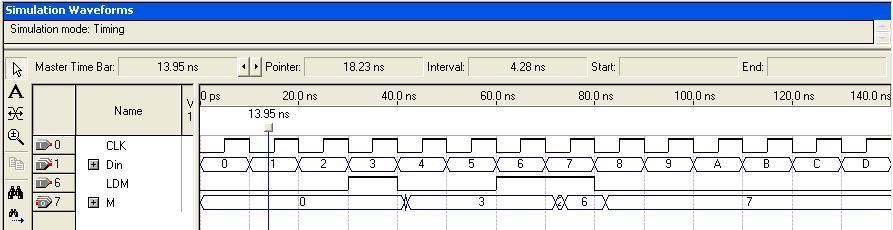
8 5. To support Data Transfer Operations, registers should have the capability to receive data in parallel (parallel load). The load control input when active enables the data at the data inputs to be loaded in parallel on the next clock pulse. Din Load clk Dout 8
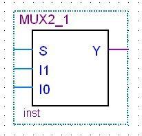
9 6. Data Transfer Operations. To support instructions that moves data between registers (to support arithmetic operations), various registers must be organized (interconnected) to facilitate the transfer of data. Data Routing Circuits, route data from source registers to the inputs of all registers. Source registers are selected by multiplexers and the target register is selected by a decoder. DECODER MXN 1 destination select 2 N N - 1 MUX Reg Reg1 1 Reg2 2 RegN N Y source select 9
10 Summary: the instruction set of a digital computer defines the set of operation its datapath can support. instructions defines the characteristics and capabilities of the processing elements of the datapath. arithmetic instructions such as addition and subtraction can be implemented using adder and subtractor circuit. registers are provided to hold data needed by arithmetic circuits. computer cycles involve the fetch cycle and the execute cycle. registers are organized to facilitate transfer of data to required parts of the system. 1
11 Control Unit Reset Control Signals Combinational Network Memory (State) 11
12 Reset Control Unit Datapath Combinational Network (Binary Multiplier) Memory (State) 12
13 Reset Control Unit Datapath Combinational Network General Purpose Processor Instruction Set Architecture Complex Instruction Set Computer Direct Addressing Mode Memory (State) 13
14 (General Data Processor): Fetch Cycle Control Unit Reset Combinational Network Memory (State) Datapath IR PC Memory 14
15 (General Data Processor) : Execute Cycle Control Unit Reset Combinational Network Memory (State) Datapath IR PC Memory ACC TMP Processing Elements +/su 15
16 (General Data Processor) : Execute Cycle Control Unit Reset Combinational Network Datapath IR PC Data Routing circuits Memory (State) Memory ACC TMP Processing Elements +/su 16
17 Simple As Possible Computer (SAP) 17
18 Simple As Possible Computer (SAP) MEMORY 18
19 Simple As Possible Computer (SAP) Fetch Cycle Elements 19
20 Simple As Possible Computer (SAP) Processing Elements (EXecute Cycle) 2
 Data Routing Circuits")
21 Simple As Possible Computer (SAP) Data Routing Circuits 21
22 Parts of a Digital Computer Control Unit Memory Unit Central Processing Unit InputOutput Unit 22
23 23

24 Read Only Memory 24

25 Memory Address Register 25
26 2-1 MULTIPLEXER 26

27 ALU -Arithmetic Logic Unit 27
28 Adder/Subtractor Circuit 28
29 29

30 8-BIT REGISTERS 3

31 8-BIT REGISTER TIMING 31
32 32
33 33
34 34
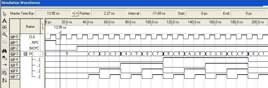
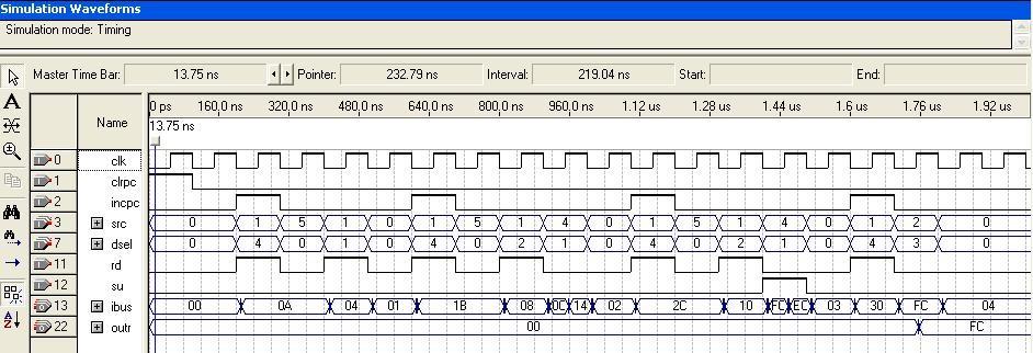
35 clrpc incpc dessel srcsel rd su 1 ' ' PC CLEAR PC or reset ' ' MAR PC PC to MAR 1' 1' 1 IR M[MAR] MEMORY TO IR (opcode fetch) 1 ' ' PC PC + 1 INCrement PC ' 11 MAR IR[3:] IR TO MAR Transfer operand 1' 1' 1 A M[MAR] MEMory to ACC memory read to A 1' 1' 1 B M[MAR] MEMory to B memory read to B 1' 1' A A+ B ALU to ACC (addition) 1' 1' 1 A A- B ALU to ACC (subtraction) 11' 1' OUTR A ACC to OUTR Micro operations Description 35
36 clrpc incpc dessel srcsel rd su Hexcode Micro operations RESET 1 ' ' 2 PC Fetch Cycle ' ' ' MAR PC 1 1' 1' IR M[MAR], PC PC + 1 LDA ' 11 1' MAR IR[3:] 1' 1' 1 26' A M[MAR], goto Fetch ADD ' 11 1' MAR IR[3:] 1' 1' 1 46' B M[MAR] 1' 1' 3' A A + B, goto Fetch SUB ' 11 1' MAR IR[3:] 1' 1' 1 46' B M[MAR] 1' 1' 1 31' A A - B, goto Fetch OUT 11' 1' 68' OUTR A, goto Fetch HLT ' ' ' enstate 36
37 37
38 Designing the Simple As Possible Computer Control Unit Memory Unit THANK YOU Central Processing Unit InputOutput Unit 38
COMARCH. COMPUTER ARCHITECTURE TERM 3 SY COMPUTER ENGINEERING DE LA SALLE UNIVERSITY Quiz 1
 COMARCH. COMPUTER ARCHITECTURE TERM 3 SY 2015 2016 COMPUTER ENGINEERING DE LA SALLE UNIVERSITY Quiz 1 1. Draw the logic symbol of the component whose operations are specified by the following microoperations:
Register Transfer and Micro-operations
 Register Transfer Language Register Transfer Bus Memory Transfer Micro-operations Some Application of Logic Micro Operations Register Transfer and Micro-operations Learning Objectives After reading this
CHAPTER SIX BASIC COMPUTER ORGANIZATION AND DESIGN
 CHAPTER SIX BASIC COMPUTER ORGANIZATION AND DESIGN 6.1. Instruction Codes The organization of a digital computer defined by: 1. The set of registers it contains and their function. 2. The set of instructions
Chapter 5. Computer Architecture Organization and Design. Computer System Architecture Database Lab, SANGJI University
 Chapter 5. Computer Architecture Organization and Design Computer System Architecture Database Lab, SANGJI University Computer Architecture Organization and Design Instruction Codes Computer Registers
REGISTER TRANSFER LANGUAGE
 REGISTER TRANSFER LANGUAGE The operations executed on the data stored in the registers are called micro operations. Classifications of micro operations Register transfer micro operations Arithmetic micro
COMPUTER ORGANIZATION
 COMPUTER ORGANIZATION INDEX UNIT-II PPT SLIDES Srl. No. Module as per Session planner Lecture No. PPT Slide No. 1. Register Transfer language 2. Register Transfer Bus and memory transfers 3. Arithmetic
SCRAM Introduction. Philipp Koehn. 19 February 2018
 SCRAM Introduction Philipp Koehn 19 February 2018 This eek 1 Fully work through a computer circuit assembly code Simple but Complete Random Access Machine (SCRAM) every instruction is 8 bit 4 bit for op-code:
Outcomes. Lecture 13 - Introduction to the Central Processing Unit (CPU) Central Processing UNIT (CPU) or Processor
 Central Processing UNIT (CPU) or Processor") Lecture 13 - Introduction to the Central Processing Unit (CPU) Outcomes What is a CPU? How are instructions prepared by the CPU before execution? What registers and operations are involved in this preparation
Lecture 13 - Introduction to the Central Processing Unit (CPU) Outcomes What is a CPU? How are instructions prepared by the CPU before execution? What registers and operations are involved in this preparation
Department of Computer and Mathematical Sciences. Lab 4: Introduction to MARIE
 Department of Computer and Mathematical Sciences CS 3401 Assembly Language 4 Lab 4: Introduction to MARIE Objectives: The main objective of this lab is to get you familiarized with MARIE a simple computer
CS 265. Computer Architecture. Wei Lu, Ph.D., P.Eng.
 CS 265 Computer Architecture Wei Lu, Ph.D., P.Eng. Part 3: von Neumann Architecture von Neumann Architecture Our goal: understand the basics of von Neumann architecture, including memory, control unit
REGISTER TRANSFER AND MICROOPERATIONS
 REGISTER TRANSFER AND MICROOPERATIONS Register Transfer Language Register Transfer Bus and Memory Transfers Arithmetic Microoperations Logic Microoperations Shift Microoperations Arithmetic Logic Shift
Computer Organization II CMSC 3833 Lecture 33
 Term MARIE Definition Machine Architecture that is Really Intuitive and Easy 4.8.1 The Architecture Figure s Architecture Characteristics: Binary, two s complement Stored program, fixed word length Word
REGISTER TRANSFER AND MICROOPERATIONS
 1 REGISTER TRANSFER AND MICROOPERATIONS Register Transfer Language Register Transfer Bus and Memory Transfers Arithmetic Microoperations Logic Microoperations Shift Microoperations Arithmetic Logic Shift
Chapter 4. The Processor
 Chapter 4 The Processor Introduction CPU performance factors Instruction count Determined by ISA and compiler CPI and Cycle time Determined by CPU hardware We will examine two MIPS implementations A simplified
16.1. Unit 16. Computer Organization Design of a Simple Processor
 6. Unit 6 Computer Organization Design of a Simple Processor HW SW 6.2 You Can Do That Cloud & Distributed Computing (CyberPhysical, Databases, Data Mining,etc.) Applications (AI, Robotics, Graphics, Mobile)
Processor (I) - datapath & control. Hwansoo Han
 - datapath & control. Hwansoo Han") Processor (I) - datapath & control Hwansoo Han Introduction CPU performance factors Instruction count - Determined by ISA and compiler CPI and Cycle time - Determined by CPU hardware We will examine two
Processor (I) - datapath & control Hwansoo Han Introduction CPU performance factors Instruction count - Determined by ISA and compiler CPI and Cycle time - Determined by CPU hardware We will examine two
UNIT-III REGISTER TRANSFER LANGUAGE AND DESIGN OF CONTROL UNIT
 UNIT-III 1 KNREDDY UNIT-III REGISTER TRANSFER LANGUAGE AND DESIGN OF CONTROL UNIT Register Transfer: Register Transfer Language Register Transfer Bus and Memory Transfers Arithmetic Micro operations Logic
The Processor: Datapath and Control. Jin-Soo Kim Computer Systems Laboratory Sungkyunkwan University
 The Processor: Datapath and Control Jin-Soo Kim (jinsookim@skku.edu) Computer Systems Laboratory Sungkyunkwan University http://csl.skku.edu Introduction CPU performance factors Instruction count Determined
CHAPTER 4: Register Transfer Language and Microoperations
 CS 224: Computer Organization S.KHABET CHAPTER 4: Register Transfer Language and Microoperations Outline Register Transfer Language Register Transfer Bus and Memory Transfers Arithmetic Microoperations
C.P.U Organization. Memory Unit. Central Processing Unit (C.P.U) Input-Output Processor (IOP) Figure (1) Digital Computer Block Diagram
 Input-Output Processor (IOP) Figure (1) Digital Computer Block Diagram") C.P.U Organization 1.1 Introduction A computer system is sometimes subdivided into two functional entities "Hardware" and "Software". The H/W of the computer consists of all the electronic components and
C.P.U Organization 1.1 Introduction A computer system is sometimes subdivided into two functional entities "Hardware" and "Software". The H/W of the computer consists of all the electronic components and
CPU ARCHITECTURE. QUESTION 1 Explain how the width of the data bus and system clock speed affect the performance of a computer system.
 CPU ARCHITECTURE QUESTION 1 Explain how the width of the data bus and system clock speed affect the performance of a computer system. ANSWER 1 Data Bus Width the width of the data bus determines the number
Computer architecture Assignment 3
 Computer architecture Assignment 3 1- An instruction at address 14E in the basic computer has I=0, an operation code of the AND instruction, and an address part equal to 109(all numbers are in hexadecimal).
COMPUTER ARCHITECTURE AND ORGANIZATION Register Transfer and Micro-operations 1. Introduction A digital system is an interconnection of digital
 Register Transfer and Micro-operations 1. Introduction A digital system is an interconnection of digital hardware modules that accomplish a specific information-processing task. Digital systems vary in
csitnepal Unit 3 Basic Computer Organization and Design
 Unit 3 Basic Computer Organization and Design Introduction We introduce here a basic computer whose operation can be specified by the resister transfer statements. Internal organization of the computer
CISC Processor Design
 CISC Processor Design Virendra Singh Indian Institute of Science Bangalore virendra@computer.org Lecture 3 SE-273: Processor Design Processor Architecture Processor Architecture CISC RISC Jan 21, 2008
PSIM: Processor SIMulator (version 4.2)
") PSIM: Processor SIMulator (version 4.2) by Charles E. Stroud, Professor Dept. of Electrical & Computer Engineering Auburn University July 23, 2003 ABSTRACT A simulator for a basic stored program computer
PSIM: Processor SIMulator (version 4.2) by Charles E. Stroud, Professor Dept. of Electrical & Computer Engineering Auburn University July 23, 2003 ABSTRACT A simulator for a basic stored program computer
Chapter 4. The Processor
 Chapter 4 The Processor Introduction CPU performance factors Instruction count Determined by ISA and compiler CPI and Cycle time Determined by CPU hardware 4.1 Introduction We will examine two MIPS implementations
General purpose registers These are memory units within the CPU designed to hold temporary data.
 Von Neumann Architecture Single processor is used Each instruction in a program follows a linear sequence of fetch decode execute cycle Program and data are held in same main memory Stored program Concept
Computer Organization and Design
 CSE211 Computer Organization and Design Lecture : 3 Tutorial: 1 Practical: 0 Credit: 4 KIDS Labs 1 Unit 1 : Basics of Digital Electronics Introduction Logic Gates Flip Flops Decoder Encoder Multiplexers
Faculty of Engineering Systems & Biomedical Dept. First Year Cairo University Sheet 6 Computer I
 aculty of Engineering Systems & Biomedical Dept. irst Year Cairo University Sheet 6 Computer I 1. Choose rue or alse for each of the following statements a) In a direct addressing mode instruction, the
Note that none of the above MAY be a VALID ANSWER.
 ECE 270 Learning Outcome 4-1 - Practice Exam / Solution OUTCOME #4: An ability to design and implement computer logic circuits. Multiple Choice select the single most appropriate response for each question.
Blog -
 . Instruction Codes Every different processor type has its own design (different registers, buses, microoperations, machine instructions, etc) Modern processor is a very complex device It contains Many
Basics of Microprocessor
 Unit 1 Basics of Microprocessor 1. Microprocessor Microprocessor is a multipurpose programmable integrated device that has computing and decision making capability. This semiconductor IC is manufactured
CS222: Processor Design
 CS222: Processor Design Dr. A. Sahu Dept of Comp. Sc. & Engg. Indian Institute of Technology Guwahati Processor Design building blocks Outline A simple implementation: Single Cycle Data pathandcontrol
UNIT - V MEMORY P.VIDYA SAGAR ( ASSOCIATE PROFESSOR) Department of Electronics and Communication Engineering, VBIT
 Department of Electronics and Communication Engineering, VBIT") UNIT - V MEMORY P.VIDYA SAGAR ( ASSOCIATE PROFESSOR) contents Memory: Introduction, Random-Access memory, Memory decoding, ROM, Programmable Logic Array, Programmable Array Logic, Sequential programmable
UNIT - V MEMORY P.VIDYA SAGAR ( ASSOCIATE PROFESSOR) contents Memory: Introduction, Random-Access memory, Memory decoding, ROM, Programmable Logic Array, Programmable Array Logic, Sequential programmable
Teaching London Computing
 Teaching London Computing CAS London CPD Day 2016 Little Man Computer William Marsh School of Electronic Engineering and Computer Science Queen Mary University of London Overview and Aims LMC is a computer
Chapter 4. The Processor. Instruction count Determined by ISA and compiler. We will examine two MIPS implementations
 Chapter 4 The Processor Part I Introduction CPU performance factors Instruction count Determined by ISA and compiler CPI and Cycle time Determined by CPU hardware We will examine two MIPS implementations
Unit II Basic Computer Organization
 1. Define the term. Internal Organization-The internal organization of a digital system is defined by the sequence of microoperations it performs on data stored in its registers. Program- A program is
Class Notes. Dr.C.N.Zhang. Department of Computer Science. University of Regina. Regina, SK, Canada, S4S 0A2
 Class Notes CS400 Part VI Dr.C.N.Zhang Department of Computer Science University of Regina Regina, SK, Canada, S4S 0A2 C. N. Zhang, CS400 83 VI. CENTRAL PROCESSING UNIT 1 Set 1.1 Addressing Modes and Formats
ECE260: Fundamentals of Computer Engineering
 Datapath for a Simplified Processor James Moscola Dept. of Engineering & Computer Science York College of Pennsylvania Based on Computer Organization and Design, 5th Edition by Patterson & Hennessy Introduction
Computer Architecture Programming the Basic Computer
 4. The Execution of the EXCHANGE Instruction The EXCHANGE routine reads the operand from the effective address and places it in DR. The contents of DR and AC are interchanged in the third microinstruction.
Chapter 16. Control Unit Operation. Yonsei University
 Chapter 16 Control Unit Operation Contents Micro-Operation Control of the Processor Hardwired Implementation 16-2 Micro-Operations Micro-Operations Micro refers to the fact that each step is very simple
Programming Level A.R. Hurson Department of Computer Science Missouri University of Science & Technology Rolla, Missouri
 Programming Level A.R. Hurson Department of Computer Science Missouri University of Science & Technology Rolla, Missouri 65409 hurson@mst.edu A.R. Hurson 1 Programming Level Computer: A computer with a
CHAPTER 5 Basic Organization and Design Outline Instruction Codes Computer Registers Computer Instructions Timing and Control Instruction Cycle
 CS 224: Computer Organization S.KHABET CHAPTER 5 Basic Organization and Design Outline Instruction Codes Computer Registers Computer Instructions Timing and Control Instruction Cycle Memory Reference Instructions
CN310 Microprocessor Systems Design
 CN310 Microprocessor Systems Design Simple Computer Nawin Somyat Department of Electrical and Computer Engineering Thammasat University Outline Course Contents 1 Introduction 2 Simple Computer 3 Microprocessor
Chapter 4. The Processor Designing the datapath
 Chapter 4 The Processor Designing the datapath Introduction CPU performance determined by Instruction Count Clock Cycles per Instruction (CPI) and Cycle time Determined by Instruction Set Architecure (ISA)
5-1 Instruction Codes
 Chapter 5: Lo ai Tawalbeh Basic Computer Organization and Design 5-1 Instruction Codes The Internal organization of a digital system is defined by the sequence of microoperations it performs on data stored
Combinational and sequential circuits (learned in Chapters 1 and 2) can be used to create simple digital systems.
 can be used to create simple digital systems.") REGISTER TRANSFER AND MICROOPERATIONS Register Transfer Language Register Transfer Bus and Memory Transfers Arithmetic Microoperations Logic Microoperations Shift Microoperations Arithmetic Logic Shift
REGISTER TRANSFER AND MICROOPERATIONS Register Transfer Language Register Transfer Bus and Memory Transfers Arithmetic Microoperations Logic Microoperations Shift Microoperations Arithmetic Logic Shift
THE MICROPROCESSOR Von Neumann s Architecture Model
 THE ICROPROCESSOR Von Neumann s Architecture odel Input/Output unit Provides instructions and data emory unit Stores both instructions and data Arithmetic and logic unit Processes everything Control unit
Block diagram view. Datapath = functional units + registers
 Computer design an application of digital logic design procedures Computer = processing unit + memory system Processing unit = control + datapath Control = finite state machine inputs = machine instruction,
BASIC COMPUTER ORGANIZATION AND DESIGN
 1 BASIC COMPUTER ORGANIZATION AND DESIGN Instruction Codes Computer Registers Computer Instructions Timing and Control Instruction Cycle Memory Reference Instructions Input-Output and Interrupt Complete
Pin Description, Status & Control Signals of 8085 Microprocessor
 Pin Description, Status & Control Signals of 8085 Microprocessor 1 Intel 8085 CPU Block Diagram 2 The 8085 Block Diagram Registers hold temporary data. Instruction register (IR) holds the currently executing
ASSIGNMENT ECE514 (COMPUTER ORGANIZATION) ASSIGNMENT NO. 3
 ASSIGNMENT NO. 3") ASSIGNMENT ECE514 (COMPUTER ORGANIZATION) ASSIGNMENT NO. 3 This is an individual assignment for ECE514. It carries a mark of 10%. The rubric of marks is given in Appendix 3. This assignment is about designing
ASSIGNMENT ECE514 (COMPUTER ORGANIZATION) ASSIGNMENT NO. 3 This is an individual assignment for ECE514. It carries a mark of 10%. The rubric of marks is given in Appendix 3. This assignment is about designing
Chapter 4. MARIE: An Introduction to a Simple Computer. Chapter 4 Objectives. 4.1 Introduction. 4.2 CPU Basics
 Chapter 4 Objectives Learn the components common to every modern computer system. Chapter 4 MARIE: An Introduction to a Simple Computer Be able to explain how each component contributes to program execution.
Control and Datapath 8
 Control and Datapath 8 Engineering attempts to develop design methods that break a problem up into separate steps to simplify the design and increase the likelihood of a correct solution. Digital system
Digital System Design Using Verilog. - Processing Unit Design
 Digital System Design Using Verilog - Processing Unit Design 1.1 CPU BASICS A typical CPU has three major components: (1) Register set, (2) Arithmetic logic unit (ALU), and (3) Control unit (CU) The register
Basic Computer Organization - Designing your first computer. Acknowledgment: Most of the slides are adapted from Prof. Hyunsoo Yoon s slides.
 Basic Computer Organization - Designing your first computer Acknowledgment: Most of the slides are adapted from Prof. Hyunsoo Yoon s slides. 1 This week- BASIC COMPUTER ORGANIZATION AND DESIGN Instruction
Little Man Computer (LMC)
") Little Man Computer (LMC) A-level Computing Independent Study Project Part Two The Little Man Computer (LMC) is a simulator which models the basic features of a modern computer. It features a central processing
Little Man Computer (LMC) A-level Computing Independent Study Project Part Two The Little Man Computer (LMC) is a simulator which models the basic features of a modern computer. It features a central processing
MICROPROCESSOR AND MICROCONTROLLER BASED SYSTEMS
 MICROPROCESSOR AND MICROCONTROLLER BASED SYSTEMS UNIT I INTRODUCTION TO 8085 8085 Microprocessor - Architecture and its operation, Concept of instruction execution and timing diagrams, fundamentals of
Memory General R0 Registers R1 R2. Input Register 1. Input Register 2. Program Counter. Instruction Register
 CPU Organisation Central Processing Unit (CPU) Memory General R0 Registers R1 R2 ALU R3 Output Register Input Register 1 Input Register 2 Internal Bus Address Bus Data Bus Addr. $ 000 001 002 Program Counter
MICROCOMPUTER OPERATION
 CET270 Intro to Microprocessors Notes 3 MICROCOMPUTER OPERATION Previously, we covered basics of microcomputers including terminology and simplified computer and processor architectural diagrams. Now we
Fundamentals of Computer Architecture. 8. Bringing It All Together The Hardware Engineer s Perspective
 Fundamentals of Computer Architecture 8. Bringing It All Together The Hardware Engineer s Perspective 1 CHAPTER OVERVIEW This chapter includes: Assigning tasks to individual processor components; Micro-instructions;
Advanced Parallel Architecture Lesson 3. Annalisa Massini /2015
 Advanced Parallel Architecture Lesson 3 Annalisa Massini - 2014/2015 Von Neumann Architecture 2 Summary of the traditional computer architecture: Von Neumann architecture http://williamstallings.com/coa/coa7e.html
BASIC COMPUTER ORGANIZATION AND DESIGN
 1 BASIC COMPUTER ORGANIZATION AND DESIGN Instruction Codes Computer Registers Computer Instructions Timing and Control Instruction Cycle Memory Reference Instructions Input-Output and Interrupt Complete
EXPERIMENT NO. 1 THE MKT 8085 MICROPROCESSOR TRAINER
 OBJECT: EXPERIMENT NO. 1 THE MKT 8085 MICROPROCESSOR TRAINER To understand the structure and operating instruction of the microprocessor trainer. INTRODUCTION: The MKT 8085 is a single-board microcomputer,
The MIPS Processor Datapath
 The MIPS Processor Datapath Module Outline MIPS datapath implementation Register File, Instruction memory, Data memory Instruction interpretation and execution. Combinational control Assignment: Datapath
Computer Organization (Autonomous)
") Computer Organization (Autonomous) UNIT II Sections - A & D Prepared by Anil Kumar Prathipati, Asst. Prof., Dept. of CSE. SYLLABUS Basic Computer Organization and Design: Instruction codes Stored Program
Computer Organization (Autonomous) UNIT II Sections - A & D Prepared by Anil Kumar Prathipati, Asst. Prof., Dept. of CSE. SYLLABUS Basic Computer Organization and Design: Instruction codes Stored Program
Assembly Language Programming of 8085
 Assembly Language Programming of 8085 Topics 1. Introduction 2. Programming model of 8085 3. Instruction set of 8085 4. Example Programs 5. Addressing modes of 8085 6. Instruction & Data Formats of 8085
A3 Computer Architecture
 A3 Computer Architecture Engineering Science 3rd year A3 Lectures Prof David Murray david.murray@eng.ox.ac.uk www.robots.ox.ac.uk/ dwm/courses/3co Michaelmas 2000 1 / 1 2: Introduction to the CPU 3A3 Michaelmas
The Itanium Bit Microprocessor Report
 The Itanium - 1986 8 Bit Microprocessor Report By PRIYANK JAIN (02010123) Group # 11 Under guidance of Dr. J. K. Deka & Dr. S. B. Nair Department of Computer Science & Engineering Indian Institute of Technology,
Instruction : A command to the microprocessor to perform a given task on specified data. Each instruction has two parts
 Lecture 4 Instruction : A command to the microprocessor to perform a given task on specified data. Each instruction has two parts One part is the task to be performed, called operation code or opcode in
The Processor (1) Jinkyu Jeong Computer Systems Laboratory Sungkyunkwan University
 Jinkyu Jeong Computer Systems Laboratory Sungkyunkwan University") The Processor (1) Jinkyu Jeong (jinkyu@skku.edu) Computer Systems Laboratory Sungkyunkwan University http://csl.skku.edu EEE3050: Theory on Computer Architectures, Spring 2017, Jinkyu Jeong (jinkyu@skku.edu)
The Processor (1) Jinkyu Jeong (jinkyu@skku.edu) Computer Systems Laboratory Sungkyunkwan University http://csl.skku.edu EEE3050: Theory on Computer Architectures, Spring 2017, Jinkyu Jeong (jinkyu@skku.edu)
Computer Architecture
 University of Craiova Faculty of Automation, Computers & Electronics Department of Computers & Information Technology Computer Architecture Elementary Educational Computer (EEC) Cătălina Mancaș catalina.mancas@yahoo.it
Chapter 2 Instruction Set Architecture
 Chapter 2 Instruction Set Architecture Course Outcome (CO) - CO2 Describe the architecture and organization of computer systems Program Outcome (PO) PO1 Apply knowledge of mathematics, science and engineering
CS 31: Intro to Systems Digital Logic. Kevin Webb Swarthmore College February 3, 2015
 CS 31: Intro to Systems Digital Logic Kevin Webb Swarthmore College February 3, 2015 Reading Quiz Today Hardware basics Machine memory models Digital signals Logic gates Circuits: Borrow some paper if
STRUCTURE OF DESKTOP COMPUTERS
 Page no: 1 UNIT 1 STRUCTURE OF DESKTOP COMPUTERS The desktop computers are the computers which are usually found on a home or office desk. They consist of processing unit, storage unit, visual display
Computer Organization (Autonomous)
") Computer Organization (Autonomous) UNIT I Sections - A & D Prepared by Anil Kumar Prathipati, Asst. Prof., Dept. of CSE. SYLLABUS Introduction: Types of Computers, Functional units of Basic Computer (Block
Computer Organization (Autonomous) UNIT I Sections - A & D Prepared by Anil Kumar Prathipati, Asst. Prof., Dept. of CSE. SYLLABUS Introduction: Types of Computers, Functional units of Basic Computer (Block
EE 2700 Project 2 Microprocessor Design
 EE 2700 Project 2 Microprocessor Design This project may be done individually or in teams of two. You may consult others for general questions but not for specific issues. Cheating will not be tolerated
The functional block diagram of 8085A is shown in fig.4.1.
 Lecture-13 Internal Architecture of Intel 05A The functional block diagram of 05A is shown in fig.4.1. INTA INTR RST7.5 RST5.5 RST6.5 TRAP SOD SID INTERRUPT SERIAL I/O (Internal Bus) FR(S) IR() B() C()
BASIC COMPUTER ORGANIZATION AND DESIGN
 BASIC COMPUTER ORGANIZATION AND DESIGN Instruction Codes Computer Registers Computer Instructions Timing and Control Instruction Cycle Memory Reference Instructions Input-Output and Interrupt Complete
CS 31: Intro to Systems Digital Logic. Kevin Webb Swarthmore College February 2, 2016
 CS 31: Intro to Systems Digital Logic Kevin Webb Swarthmore College February 2, 2016 Reading Quiz Today Hardware basics Machine memory models Digital signals Logic gates Circuits: Borrow some paper if
Section 6. Memory Components Chapter 5.7, 5.8 Physical Implementations Chapter 7 Programmable Processors Chapter 8
 Section 6 Memory Components Chapter 5.7, 5.8 Physical Implementations Chapter 7 Programmable Processors Chapter 8 Types of memory Two major types of memory Volatile When power to the device is removed
Lecture1: introduction. Outline: History overview Central processing unite Register set Special purpose address registers Datapath Control unit
 Lecture1: introduction Outline: History overview Central processing unite Register set Special purpose address registers Datapath Control unit 1 1. History overview Computer systems have conventionally
COMPUTER ORGANIZATION AND DESIGN. 5 th Edition. The Hardware/Software Interface. Chapter 4. The Processor
 COMPUTER ORGANIZATION AND DESIGN The Hardware/Software Interface 5 th Edition Chapter 4 The Processor Introduction CPU performance factors Instruction count Determined by ISA and compiler CPI and Cycle
Laboratory 5 Processor Datapath
 Laboratory 5 Processor Datapath Description of HW Instruction Set Architecture 16 bit data bus 8 bit address bus Starting address of every program = 0 (PC initialized to 0 by a reset to begin execution)
CO Computer Architecture and Programming Languages CAPL. Lecture 9
 CO20-320241 Computer Architecture and Programming Languages CAPL Lecture 9 Dr. Kinga Lipskoch Fall 2017 A Four-bit Number Circle CAPL Fall 2017 2 / 38 Functional Parts of an ALU CAPL Fall 2017 3 / 38 Addition
Computer Architecture and Organization: L04: Micro-operations
 Computer Architecture and Organization: L4: Micro-operations By: A. H. Abdul Hafez Abdul.hafez@hku.edu.tr, ah.abdulhafez@gmail.com, hafez@research.iiit.ac.in 1 Outlines 1. Arithmetic microoperation 2.
Processing Unit CS206T
 Processing Unit CS206T Microprocessors The density of elements on processor chips continued to rise More and more elements were placed on each chip so that fewer and fewer chips were needed to construct
Digital Circuit Design and Language. Datapath Design. Chang, Ik Joon Kyunghee University
 Digital Circuit Design and Language Datapath Design Chang, Ik Joon Kyunghee University Typical Synchronous Design + Control Section : Finite State Machine + Data Section: Adder, Multiplier, Shift Register
For more notes of DAE
 Created by ARSLAN AHMED SHAAD ( 1163135 ) AND MUHMMAD BILAL ( 1163122 ) VISIT : www.vbforstudent.com Also visit : www.techo786.wordpress.com For more notes of DAE CHAPTER #6 Intel 8088/86 System Timing
Computers and Microprocessors. Lecture 34 PHYS3360/AEP3630
 Computers and Microprocessors Lecture 34 PHYS3360/AEP3630 1 Contents Computer architecture / experiment control Microprocessor organization Basic computer components Memory modes for x86 series of microprocessors
Chapter 4. MARIE: An Introduction to a Simple Computer
 Chapter 4 MARIE: An Introduction to a Simple Computer Chapter 4 Objectives Learn the components common to every modern computer system. Be able to explain how each component contributes to program execution.
Microcomputer Architecture and Programming
 IUST-EE (Chapter 1) Microcomputer Architecture and Programming 1 Outline Basic Blocks of Microcomputer Typical Microcomputer Architecture The Single-Chip Microprocessor Microprocessor vs. Microcontroller
Introduction to CPU Design
 ١ Introduction to CPU Design Computer Organization & Assembly Language Programming Dr Adnan Gutub aagutub at uqu.edu.sa [Adapted from slides of Dr. Kip Irvine: Assembly Language for Intel-Based Computers]
CHAPTER 5 : Introduction to Intel 8085 Microprocessor Hardware BENG 2223 MICROPROCESSOR TECHNOLOGY
 CHAPTER 5 : Introduction to Intel 8085 Hardware BENG 2223 MICROPROCESSOR TECHNOLOGY The 8085A(commonly known as the 8085) : Was first introduced in March 1976 is an 8-bit microprocessor with 16-bit address
Processor: Multi- Cycle Datapath & Control
 Processor: Multi- Cycle Datapath & Control (Based on text: David A. Patterson & John L. Hennessy, Computer Organization and Design: The Hardware/Software Interface, 3 rd Ed., Morgan Kaufmann, 27) COURSE
DC57 COMPUTER ORGANIZATION JUNE 2013
 Q2 (a) How do various factors like Hardware design, Instruction set, Compiler related to the performance of a computer? The most important measure of a computer is how quickly it can execute programs.
1 MALP ( ) Unit-1. (1) Draw and explain the internal architecture of 8085.
 Unit-1. (1) Draw and explain the internal architecture of 8085.") (1) Draw and explain the internal architecture of 8085. The architecture of 8085 Microprocessor is shown in figure given below. The internal architecture of 8085 includes following section ALU-Arithmetic
(1) Draw and explain the internal architecture of 8085. The architecture of 8085 Microprocessor is shown in figure given below. The internal architecture of 8085 includes following section ALU-Arithmetic
Input. Output. Datapath: System for performing operations on data, plus memory access. Control: Control the datapath in response to instructions.
 path & Control Readings: 4.1-4.4 Computer Processor Devices Control Input path Output path: System for performing operations on data, plus memory access. Control: Control the datapath in response to instructions.
Register-Level Design
 Register-Level Design A digital system can be treated at different level of abstraction or compleity. So far, we have seen it at the gate level and the transistor level. At a higher level than the gate