Standardizing WSP Wafer Socket Pogo Pin Probe Cards
|
|
|
- Anne Palmer
- 6 years ago
- Views:
Transcription


1 John Hite Texas Instruments Standardizing WSP Wafer Socket Pogo Pin Probe Cards June 6 to 9, 2010 San Diego, CA USA
2 Agenda Introduction WLCSP and WSP Probing WSP Standardization Standard Alignment / Mounting Ring FEATURES PROCEDURES Summary Next Steps Acknowledgements June 6 to 9, 2010 IEEE SW Test Workshop 2
3 Introduction Recent growth of WLCSP Wafer Level Chip Size Package probing created an opportunity for probe card hardware standardization on new WSP probe card technology. A majority of WSP socket vendors did not have established design parameters for probe heads and probe cards. As a result, standard probe head and assembly hardware were developed to drive 2 main objectives: Provide TI Business Units and Test Floors a competitive WSP probe technology based on multiple supplier sources, rather than custom solutions. Provide an opportunity to Probe Card suppliers to enter and compete directly in terms of their probe head technology and manufacturing strengths. June 6 to 9, 2010 IEEE SW Test Workshop 3


4 WLCSP and WSP Texas Instruments has been successfully integrating WSP- Wafer Socket Probe technology; primarily for WLCSP- Wafer Level Chip Size Packages using solder bump interconnections into TI and Sub-Con Test Floors. 400 µm pitch RDL Al BUMP Bump UBM Nitride Silicon PI2 PI1 WSP is categorized into (4) major wafer-level probing applications, from 400 to 150µm pitch on 250 to 75µm diameter solder bumps and Al pads. RF-Radio Frequency NRF-Non RF NRF-Non RF w/ Kelvin FC-Flip Chip June 6 to 9, 2010 IEEE SW Test Workshop 4

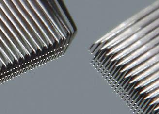

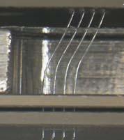
5 WLCSP Probing Technologies Cantilever Vertical Probe Card WSP Pogo-pin F F F D D D SELF-ALIGNS June 6 to 9, 2010 IEEE SW Test Workshop 5
6 WSP Major Attributes Self-Aligning 4 pts Bump Damage < VPC No Reflow Required Hand-Test Capable Lifetime > 3 M TDs PC Analyzer Not Req d. Single-pin repairable CRes < VPC Cost ~85% of VPC Cleaning < VPC Kelvin Capable 400um Deflection > VPC Force < VPC Interchangeable June 6 to 9, 2010 IEEE SW Test Workshop 6


7 Problem Statement No consistency across existing designs, sizes or shapes; Each requires a custom design. Inability to exchange heads from one vendor to another or transfer to another PCB design. June 6 to 9, 2010 IEEE SW Test Workshop 7
8 WSP Standardization Attributes INTERCHANGEABILITY: Incorporates precise alignment features and assembly hardware enabling both WSP Probe Head exchanges and overall hardware reusability. REDUCES PROBE CARD COSTS: A new PCB design is not required when a WSP probe head is changed. WSP Probe Heads from multiple vendors can be utilized on the same card allowing for multiple sourcing. SIMPLIFIES PROBE CARD DESIGN: Design of the probe card is simplified by having a single layout based on the size of the array and the X, Y coordinates of each probed pad. The layout allows the probe head to be vendor manufacturingindependent. June 6 to 9, 2010 IEEE SW Test Workshop 8
9 Collaborative Approach Reviewed conventional C VPC and prototype WSP probe heads designs to develop a standard PCB to WSP probe head interconnection across various WLCSP array patterns, sizes, multi sites, component space and PCB footprint requirements. Collaborated with TI Probe Technologists, Business Unit Test Engineers, Test Floor Operations and WSP Socket Vendors to arrive at a standard that all could support. June 6 to 9, 2010 IEEE SW Test Workshop 9

10 WSP Standardization Features WSP Probe Head Outline / Orientation Probe head to probe card alignment Component Cavities Pogo Length PCB Layout Multisite Layout Pogo Pad size Mounting holes Alignment holes Pad/Pin Alignment Keep Out Areas WSP Probe Head PCB Mounting- Alignment Ring Probes Pogo-Pin Probes 1 x 16 Array WSP Probe Card June 6 to 9, 2010 IEEE SW Test Workshop 10
11 Standard Design Basis WSP standard was based on current C VPC Heads Outer mounting ring with inner probe head Well understood on TI test floors and w/supplier base Three (3) mounting ring sizes selected to accommodate most WLCSP footprints, while allowing for component space and test cell requirements. Both mechanical and visual (ocular) alignment features were used based upon the pitch of the device. June 6 to 9, 2010 IEEE SW Test Workshop 11
12 WSP Mounting Ring Sizes 3.2 Standard Maximum Array Sizes up to 42mm x 42mm 2.25 Standard Maximum Array Sizes up to 28mm x 28mm 1.25 Standard Maximum Array Sizes up to 17mm x 17mm NOTE: A STANDARD STIFFENER IS ALSO PART OF THE HARDWARE CONFIGURATION ACROSS EACH OF THESE MOUNTING RINGS. June 6 to 9, 2010 IEEE SW Test Workshop 12
 Holes for Alignment Pins for Mounting Ring (thru) Hole for Alignment Pin for Probe Head (thru) (6) Screw Holes for Mounting Ring (tap) Mounting Ledge for the Probe Head Pin Array Space")
13 WSP Standard Mounting / Alignment Features 3.2 Standard (2) Holes for Alignment Pins for Mounting Ring (thru) Hole for Alignment Pin for Probe Head (thru) (6) Screw Holes for Mounting Ring (tap) Mounting Ledge for the Probe Head Pin Array Space (8) Screw Holes for Probe Head (tap) Hole for Alignment Pin for Probe Head (slotted) (4) Screw Holes for Test Lid Attachment (thru) June 6 to 9, 2010 IEEE SW Test Workshop 13

14 WSP Probe Head to Mounting / Alignment Ring Exploded View PROBE HEAD VENDOR DESIGN Probe unit Lower probe unit Interface Ring Mounting Ring Insulator Probe Card TI STANDARD DESIGN Insulator Alignment pin Stiffener June 6 to 9, 2010 IEEE SW Test Workshop 14
15 Mechanical Standard Alignment when pitch is > 400um. Mounting ring pinned to PCB Probe head pinned to mounting ring Relies on pin to hole tolerances No specialized assembly Attach and go June 6 to 9, 2010 IEEE SW Test Workshop 15
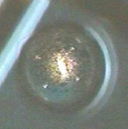
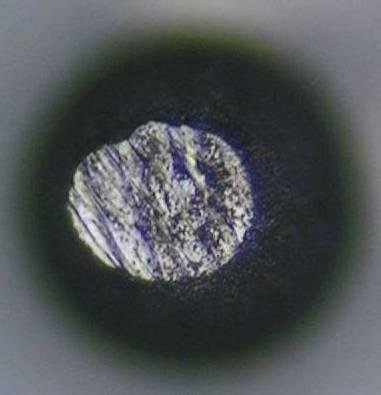
16 Visual Ocular Standard Alignment PCB uses fiducials Visual site holes in probe head Requires trained assembler when pitch is < 300um. Once procedure is completed, both the probe head and mounting ring is aligned to the PCB pad footprint. Any probe head for the same device can be exchanged with no further adjustment to the mounting required. 5 Fiducial Pads on PCB Looking through Probe Head Site Hole Probe Head + Mounting ring misaligned Both Aligned to PCB June 6 to 9, 2010 IEEE SW Test Workshop 16


17 WSP Mounting / Alignment Ring Assembly Mounting Ring Probe Head PCB Fiducial June 6 to 9, 2010 IEEE SW Test Workshop 17
18 SUMMARY Standardization has enabled TI to better integrate WSP probe card technology and multiple probe head suppliers on to TI test floors. As a result, standardization of mounting/alignment and assembly hardware has improved WSP Probe Card COO-cost of ownership in terms of: - PCB Single Design (facilitated re-orders) - Probe Head Cost (multi-source competition) - Test Floor Operations (interchangeability) June 6 to 9, 2010 IEEE SW Test Workshop 18


19 NEXT STEPS Standardization is expected to be further deployed across more device applications requiring wafer-level probing of both Bump and Pad test point features, not only for WSP, but also for conventional and advanced probe head technologies. WLCSP 400um Pitch, 250um Dia. Spherical Bump FLIP CHIP 150um Pitch, 130um Dia. Mushroom Bump FLIP CHIP 150um Pitch, 75 um Dia. Spherical Bump June 6 to 9, 2010 IEEE SW Test Workshop 19
20 ACKNOWLEDGEMENTS Norman Armendariz James Tong John Wolfe Rich Lewis Minette Ohmart Michelle Gephart* Mike Korson June 6 to 9, 2010 IEEE SW Test Workshop 20
ARCHIVE Multi Level Stacked Socket - Challenges & Solutions Mike Fedde, Ranjit Patil, Ila Pal, Vinayak Panavala Ironwood Electronics
 ARCHIVE 2010 TECHNIQUES, COMPONENTS & ADVANCES FOR NEXT GENERATION TEST Next Generation CiS (Capacitor in Socket) Featuring Discrete Capacitors and Elastomer Hybrid Schemes Shaul Lupo, Omer Vikinski Intel
Very Low Cost Probe Cards A Two Piece Approach
 E Boyd Daniels & Martin Gao Texas Instruments Mitch Baumann Millennium Circuits Very Low Cost Probe Cards A Two Piece Approach June 6 to 9, 2010 San Diego, CA USA Agenda Problem Statement Scope 2 Piece
Advance Low Force Probe cards Used on Solder Flip Chip Devices. Daniel Stillman Texas Instruments Kevin Hughes FormFactor
 Advance Low Force Probe cards Used on Solder Flip Chip Devices Daniel Stillman Texas Instruments Kevin Hughes FormFactor Overview Probe Solution Requirements Material Properties and Performance Production
Review of New, Flexible MEMS Technology to Reduce Cost of Test for Multi-site Wire Bond Applications
 Review of New, Flexible MEMS Technology to Reduce Cost of Test for Multi-site Wire Bond Applications Dan Stillman Texas Instruments Ben Eldridge FormFactor Overview Project Background & Objective Probe
Advanced CSP & Turnkey Solutions. Fumio Ohyama Tera Probe, Inc.
 Advanced CSP & Turnkey Solutions Fumio Ohyama Tera Probe, Inc. Tera Probe - Corporate Overview 1. Company : Tera Probe, Inc. 2. Founded : August, 2005 3. Capital : Approx. USD118.2 million (as of March
Multi Level Stacked Socket Challenges & Solutions
 Multi Level Stacked Socket Challenges & Solutions Mike Fedde, Ranjit Patil, Ila Pal & Vinayak Panavala Ironwood Electronics 2010 BiTS Workshop March 7-10, 2010 Content Introduction Multi Level IC Configuration
Katana RFx: A New Technology for Testing High Speed RF Applications Within TI
 Katana RFx: A New Technology for Testing High Speed RF Applications Within TI Compan Logo Probe Test Solutions Manager Overview Introduction Objectives Procedures Results Summary Follow-On Work 2 Introduction
Wafer Probe card solutions
 Wafer Probe card solutions Innovative Solutions to Test Chips in the Semiconductor Industry Our long term experience in the electronic industry and our strong developing and process teams are inspired
Over 5,000 products High Performance Adapters and Sockets Many Custom Designs Engineering Electrical and Mechanical ISO9001:2008 Registration
 Overview Company Overview Over 5,000 products High Performance Adapters and Sockets Many Custom Designs Engineering Electrical and Mechanical ISO9001:2008 Registration Adapter Technology Overview Pluggable
Adapter Technologies
 Adapter Technologies Toll Free: (800) 404-0204 U.S. Only Tel: (952) 229-8200 Fax: (952) 229-8201 email: info@ironwoodelectronics.com Introduction Company Overview Over 5,000 products High Performance Adapters
Panel Discussion Chair: Michael Huebner
 Panel Discussion Chair: Michael Huebner FormFactor Inc. Panel members Panel Discussion Mark Ojeda (Spansion/Cypress) Panel: I/II Rey Rincon (Freescale) Panel: II Al Wegleitner (TI) Panel: I/II Clark Liu
Products, Services & Capabilities
 Products, Services & Capabilities Toll Free: (800) 404-0204 U.S. Only Tel: (952) 229-8200 Fax: (952) 229-8201 email: info@ironwoodelectronics.com Overview Company Overview Founded 1986 Over 5,000 products
Wafer Probe card solutions
 Wafer Probe card solutions Innovative Solutions to Test Chips in the Semiconductor Industry Our long term experience in the electronic industry and our strong developing and process teams are inspired
Application Note. Pyramid Probe Cards
 Application Note Pyramid Probe Cards Innovating Test Technologies Pyramid Probe Technology Benefits Design for Test Internal pads, bumps, and arrays High signal integrity Rf and DC on same probe card Small
Reinforcement of PCB using Advanced Stiffeners for High Pin Count Devices
 Nicolas SALLES (SV Probe) Rehan Kazmi, PhD (SV Probe) Wayne Nelson (Reid-Ashman Manufacturing) Reinforcement of PCB using Advanced Stiffeners for High Pin Count Devices 2007 San Diego, CA USA Overview
Krzysztof Dabrowiecki, Probe2000 Inc Southwest Test Conference, San Diego, CA June 08, 2004
 Structural stability of shelf probe cards Krzysztof Dabrowiecki, Probe2000 Inc Southwest Test Conference, San Diego, CA June 08, 2004 Presentation Outline Introduction Objectives Multi die applications
Hybrid Wafer Testing Probe Card
 Chris Sellathamby Scanimetrics Inc. Hybrid Wafer Testing Probe Card June 5, 2007 San Diego, CA USA Overview Existing Issues Contact Damage Challenge Wireless (Non-contact) for Data Contact Probes for Power
E-tec Socketing solutions for BGA, LGA, CGA, CSP, MLF & Gullwing chips
 E-tec Socketing solutions for BGA, LGA, CGA, CSP, MLF & Gullwing chips Available contact styles: Elastomer interposers (10 Ghz & more) Probe pin sockets (generally below 5 Ghz) Other interposer styles
Novel Precision Probe Array for Wafer Level Final Test of WLCSP Jathan Edwards
 Novel Precision Probe Array for Wafer Level Final Test of WLCSP Johnstech International Presentation Outline Introduction to IQtouch Micro Final Test Probe Arrays for 300 500 micron pitch WLCSP Compare/contrast
Patented socketing system for the BGA/CSP technology
 Patented socketing system for the BGA/CSP technology Features: ZIF handling & only 40 grams per contact after closing the socket Sockets adapt to all package styles (at present down to 0.40mm pitch): Ceramic
The Influences of Signal Matching During Multi-site Testing
 Eddie McClanahan and Al Wegleitner Texas Instruments The Influences of Signal Matching During Multi-site Testing 2007 San Diego, CA USA Agenda Background Problem Statement Objective Methodology Results
Leveraging Multiprobe Probe Card learnings to help Standardize and improve Parametric and WLR Testing
 Leveraging Multiprobe Probe Card learnings to help Standardize and improve Parametric and WLR Testing Company Logo Brandon Mair Dawn Copeland Teas Instruments Agenda Introduction Overview Similarities
Non-contact Test at Advanced Process Nodes
 Chris Sellathamby, J. Hintzke, B. Moore, S. Slupsky Scanimetrics Inc. Non-contact Test at Advanced Process Nodes June 8-11, 8 2008 San Diego, CA USA Overview Advanced CMOS nodes are a challenge for wafer
Socket Technologies
 Socket Technologies Toll Free: (800) 404-0204 U.S. Only Tel: (952) 229-8200 Fax: (952) 229-8201 email: info@ironwoodelectronics.com Introduction Company Overview Over 5,000 products High Performance Adapters
Achieving GHz Speed in Socketed BGA Devices
 IC INTERCONNECT TOPIC #102 Technical Information from Ironwood Electronics Achieving GHz Speed in Socketed BGA Devices Ila Pal Director of R&D Ironwood Electronics Background For many products designed
AT&S Company. Presentation. 3D Component Packaging. in Organic Substrate. Embedded Component. Mark Beesley IPC Apex 2012, San Diego.
 3D Component Packaging AT&S Company in Organic Substrate Presentation Embedded Component Mark Beesley IPC Apex 2012, San Diego www.ats.net Austria Technologie & Systemtechnik Aktiengesellschaft Fabriksgasse13
Wafer Level Packaging The Promise Evolves Dr. Thomas Di Stefano Centipede Systems, Inc. IWLPC 2008
 Wafer Level Packaging The Promise Evolves Dr. Thomas Di Stefano Centipede Systems, Inc. IWLPC 2008 / DEVICE 1.E+03 1.E+02 1.E+01 1.E+00 1.E-01 1.E-02 1.E-03 1.E-04 1.E-05 1.E-06 1.E-07 Productivity Gains
Key Considerations to Probe Cu Pillars in High Volume Production
 Key Considerations to Probe Cu Pillars in High Volume Production Alexander Wittig (GLOBALFOUNDRIES) Amy Leong, Tin Nguyen, Tommaso Masi, Jarek Kister, Mike Slessor (Form Factor) Overview Key Industry Trends
2688 WESTHILLS COURT, SIMI VALLEY, CA
 NEW PRODUCT INTRODUCTION 2688 WESTHILLS COURT, SIMI VALLEY, CA 93065-2635 To: All Hirose Sales Personnel and Partners From: Hirose USA Marketing Dept. Subject: New Product Release for IT11 Series October
Packaging for parallel optical interconnects with on-chip optical access
 Packaging for parallel optical interconnects with on-chip optical access I. INTRODUCTION Parallel optical interconnects requires the integration of lasers and detectors directly on the CMOS chip. In the
Low Force MEMS Probe Solution for Full Wafer Single Touch Test
 Matt Losey Yohannes Desta Melvin Khoo Lakshmikanth Namburi Georg Aigeldinger Touchdown Technologies Low Force MEMS Probe Solution for Full Wafer Single Touch Test June 6 to 9, 2010 San Diego, CA USA Towards
ARCHIVE 2008 COPYRIGHT NOTICE
 Keynote Speaker ARCHIVE 2008 Packaging & Assembly in Pursuit of Moore s Law and Beyond Karl Johnson Ph.D. Vice President and Senior Fellow Advanced Packaging Systems Integration Laboratory Freescale Semiconductor
SOFIX - A fully shielded front IO solution. Product Presentation
 - A fully shielded front IO solution Product Presentation Product Description SOFIX is a front IO interconnection system comprised of R/A headers and cable plugs, suitable for the distribution of power
Power Matters. TM. Why Embedded Die? Piers Tremlett Microsemi 22/9/ Microsemi Corporation. Company Proprietary 1
 Power Matters. TM Why Embedded Die? Piers Tremlett Microsemi 22/9/16 1 Introduction This presentation: Outlines our journey to make miniaturised SiP modules Compares : Embedded Die Technology (EDT) With
3.3 Integrate Reconfigurable Mass Interconnect Solutions. Evaluating Platforms for Performance and Reusability
 3.3 Integrate Reconfigurable Mass Interconnect Solutions Evaluating Platforms for Performance and Reusability 157 What is a MASS INTERCONNECT? Creates Order From Chaos 158 Mass Interconnect Standardize
Burn-in & Test Socket Workshop
 Burn-in & Test Socket Workshop March 6-9, 2005 Hilton Phoenix East / Mesa Hotel Mesa, Arizona ARCHIVE TM Burn-in & Test Socket Workshop TM COPYRIGHT NOTICE The papers in this publication comprise the proceedings
Socket Technologies
 Socket Technologies Introduction Company Overview Over 5,000 products High Performance Adapters and Sockets Many Custom Designs Engineering Electrical and Mechanical ISO9001:2008 Registration Socket Technology
An integrated solution for KGD: At-speed wafer-level testing and full-contact wafer-level burn-in after flip chip bumping
 An integrated solution for KGD: At-speed wafer-level testing and full-contact wafer-level burn-in after flip chip bumping Yuan-Ping Tseng/ An-Hong Liu TD center ChipMOS Technologies Inc. June 5, 2001 1
Rolling Up Solutions of Wafer Probing Technologies Joey Wu
 Rolling Up Solutions of Wafer Probing Technologies Joey Wu Manager, Global Marketing Drivers of Semiconductor Industry Source: Yole, 2016 Source: Yole, 2016 Source: Yole, 2016 Source: Yole, 2016 Form-factor
High Parallelism Memory Test Advances based on MicroSpring Contact Technology
 High Parallelism Memory Test Advances based on MicroSpring Contact Technology Thomas Homorodi- Director of Marketing Robert Martin Technical Sales Eng. Southwest Test Workshop June 2001 Contents Introduction
2 protocol and ISO/IEC C, Qstar-5R. series is. tag chips. What s. more, it. up to 30. years in. dbm [2] QSTAR FAMILY - Qstar-5R series
![2 protocol and ISO/IEC C, Qstar-5R. series is. tag chips. What s. more, it. up to 30. years in. dbm [2] QSTAR FAMILY - Qstar-5R series](/thumbs/91/107188518.jpg "2 protocol and ISO/IEC C, Qstar-5R. series is. tag chips. What s. more, it. up to 30. years in. dbm [2] QSTAR FAMILY - Qstar-5R series") - Ver. 1.011 APR24, 2017 Datasheet for Public Use Overview Conforming to EPCglobal Class 1 Gen 2 protocol 1.2.0 and ISO/IEC 18000-6C, Qstar-5R series is a highly integrated UHF RFID tag chips with industry
- Ver. 1.011 APR24, 2017 Datasheet for Public Use Overview Conforming to EPCglobal Class 1 Gen 2 protocol 1.2.0 and ISO/IEC 18000-6C, Qstar-5R series is a highly integrated UHF RFID tag chips with industry
BiTS Poster Session. March 5-8, Hilton Phoenix / Mesa Hotel Mesa, Arizona. Archive Poster BiTS Workshop Image: tonda / istock
 March 5-8, 2017 Hilton Phoenix / Mesa Hotel Mesa, Arizona Archive Poster 2017 BiTS Workshop Image: tonda / istock Copyright Notice The presentation(s)/poster(s) in this publication comprise the Proceedings
Multi-Die Packaging How Ready Are We?
 Multi-Die Packaging How Ready Are We? Rich Rice ASE Group April 23 rd, 2015 Agenda ASE Brief Integration Drivers Multi-Chip Packaging 2.5D / 3D / SiP / SiM Design / Co-Design Challenges: an OSAT Perspective
Total Inspection Solutions Ensuring Known-Good 3DIC Package. Nevo Laron, Camtek USA, Santa Clara, CA
 Total Inspection Solutions Ensuring Known-Good 3DIC Package Nevo Laron, Camtek USA, Santa Clara, CA Density Packaging Trends vs. Defect Costs Functionality Package Yield 3DIC yield statistics 101 1.00
Spring Probes and Probe Cards for Wafer-Level Test. Jim Brandes Multitest. A Comparison of Probe Solutions for an RF WLCSP Product
 AND, AT THE WAFER LEVEL For many in the industry, performing final test at the wafer level is still a novel idea. While providing some much needed solutions, it also comes with its own set of challenges.
Innovative 3D Structures Utilizing Wafer Level Fan-Out Technology
 Innovative 3D Structures Utilizing Wafer Level Fan-Out Technology JinYoung Khim #, Curtis Zwenger *, YoonJoo Khim #, SeWoong Cha #, SeungJae Lee #, JinHan Kim # # Amkor Technology Korea 280-8, 2-ga, Sungsu-dong,
BGA Socketing Systems
 DATA BOOK BGA-TECH04 (REV. 3/04) BGA Socketing Systems Search for a footprint or build a part number online at www.bgasockets.com Solutions for Virtually Any BGA Application BGA Socket Adapter System Designed
Session 2. Burn-in & Test Socket Workshop Socket Design
 Session 2 Burn-in & Test Socket Workshop 2000 Socket Design BURN-IN & TEST SOCKET WORKSHOP COPYRIGHT NOTICE The papers in this publication comprise the proceedings of the 2000 BiTS Workshop. They reflect
LCD and Camera EMI Filter Array with ESD Protection
 LCD and Camera EMI Filter Array with ESD Protection Features Six and eight channels of EMI filtering with integrated ESD protection 0.4mm pitch, 15-bump, 2.360mm x 1.053mm footprint Chip Scale Package
Cantilever Based Ultra Fine Pitch Probing
 Cantilever Based Ultra Fine Pitch Probing Christian Leth Petersen Peter Folmer Nielsen Dirch Petersen SouthWest Test Workshop San Diego, June 2004 1 About CAPRES Danish MEMS probe & interfacing venture
Burn-in & Test Socket Workshop
 Burn-in & Test Socket Workshop IEEE March 4-7, 2001 Hilton Mesa Pavilion Hotel Mesa, Arizona IEEE COMPUTER SOCIETY Sponsored By The IEEE Computer Society Test Technology Technical Council COPYRIGHT NOTICE
TSV Test. Marc Loranger Director of Test Technologies Nov 11 th 2009, Seoul Korea
 TSV Test Marc Loranger Director of Test Technologies Nov 11 th 2009, Seoul Korea # Agenda TSV Test Issues Reliability and Burn-in High Frequency Test at Probe (HFTAP) TSV Probing Issues DFT Opportunities
March 5-8, 2017 Hilton Phoenix / Mesa Hotel Mesa, Arizona Archive Session 7
 March 5-8, 2017 Hilton Phoenix / Mesa Hotel Mesa, Arizona Archive Session 7 2017 BiTS Workshop Image: tonda / istock Copyright Notice The presentation(s)/poster(s) in this publication comprise the Proceedings
Package (1C) Young Won Lim 3/20/13
 Young Won Lim 3/20/13") Copyright (c) 2011-2013 Young W. Lim. Permission is granted to copy, distribute and/or modify this document under the terms of the GNU Free Documentation License, Version 1.2 or any later version published
Copyright (c) 2011-2013 Young W. Lim. Permission is granted to copy, distribute and/or modify this document under the terms of the GNU Free Documentation License, Version 1.2 or any later version published
Package (1C) Young Won Lim 3/13/13
 Young Won Lim 3/13/13") Copyright (c) 2011-2013 Young W. Lim. Permission is granted to copy, distribute and/or modify this document under the terms of the GNU Free Documentation License, Version 1.2 or any later version published
Copyright (c) 2011-2013 Young W. Lim. Permission is granted to copy, distribute and/or modify this document under the terms of the GNU Free Documentation License, Version 1.2 or any later version published
D-SUBMINIATURE PIN-IN-PASTE CONNECTORS
 INPUT/OUTPUT CONNECTORS D-SUBMINIATURE PIN-IN-PASTE CONNECTORS OVERVIEW The D-Subminiature connectors are one of the most popular I/O solutions, addressing segments such as Telecommunications, Industrial,
Lab 9 PCB Design & Layout
 Lab 9 PCB Design & Layout ECT 224L Department of Engineering Technology Lab 9 PCB Traces Size dependent upon electrical requirements, design constraints (routing space and clearance), and trace/space resolution
Packaging of Selected Advanced Logic in 2x and 1x nodes. 1 I TechInsights
 Packaging of Selected Advanced Logic in 2x and 1x nodes 1 I TechInsights Logic: LOGIC: Packaging of Selected Advanced Devices in 2x and 1x nodes Xilinx-Kintex 7XC 7 XC7K325T TSMC 28 nm HPL HKMG planar
3D profiler for contactless probe card inspection. Rob Marcelis
 3D profiler for contactless probe card inspection Rob Marcelis 1 Content Introduction Objectives Challenges Basics DOE Results Data transformation Advantages/disadvantages Summary conclusions Follow up
Using MLOs to Build Vertical Technology Space Transformers
 Presentation to Southwest Test Workshop 2002 Using MLOs to Build Vertical Technology Space Transformers Bill Fulton and Bill Pardee Wentworth Laboratories Overview 1. Terminology 2. Benefits of MLOs vs
Miniature 2.4 GHz Vertical-Mount PCBA Antenna
 Miniature 2.4 GHz Vertical-Mount PCBA Antenna Product Description Parsec s PTA2.4-V is a miniature 2.4 GHz antenna for Bluetooth, ZigBee, and Wi-Fi with 6.4 x 15.05 x 0.15 mm ( H x W x thickness) dimensions.
MAXIMUM SOLUTIONS (2/14 -- PR606) Mill-Max Mfg. Corp. 190 Pine Hollow Road, Oyster Bay, NY Fax:
 Mill-Max Mfg. Corp. 190 Pine Hollow Road, Oyster Bay, NY Fax:") MAXIMUM SOLUTIONS Mill-Max Series 854 Single Row and 855 Double Row Pitch Surface Mount and Through-Hole Spring-Loaded Connectors and Mating Target Connectors Mill-Max has developed high density, (1,27
MAXIMUM SOLUTIONS Mill-Max Series 854 Single Row and 855 Double Row Pitch Surface Mount and Through-Hole Spring-Loaded Connectors and Mating Target Connectors Mill-Max has developed high density, (1,27
Socket Mounting Recommendations and Reflow Profile
 Purpose This document is meant to serve as a guide for mounting E-tec surface mount device (SMD) sockets to the printed circuit board (PCB). The recommendations described here are guidelines only, and
Introduction Overview Of Intel Packaging Technology
 1 1.1 Overview Of Intel Packaging Technology As semiconductor devices become significantly more comple, electronics designers are challenged to fully harness their computing power. Transistor count in
Board Design Guidelines for Intel Programmable Device Packages
 Board Design Guidelines for Intel Programmable Device Packages AN-114 2017.02.24 Subscribe Send Feedback Contents Contents 1 Board Design Guidelines for Intel Programmable Device Packages...3 1.1 Overview
LTCC (Low Temperature Co-fired Ceramic)
") LTCC (Low Temperature Co-fired Ceramic) Design Guide Line. 381, Wonchun-Dong, Paldal-Ku, Suwon City, Kyung Ki-Do, Republic of Korea Tel : 82-31-217-2500 (Ext. 470) Fax : 82-31-217-7316 Homepage : http://www.pilkorcnd.co.kr
LTCC (Low Temperature Co-fired Ceramic) Design Guide Line. 381, Wonchun-Dong, Paldal-Ku, Suwon City, Kyung Ki-Do, Republic of Korea Tel : 82-31-217-2500 (Ext. 470) Fax : 82-31-217-7316 Homepage : http://www.pilkorcnd.co.kr
Company Overview March 12, Company Overview. Tuesday, October 03, 2017
 Company Overview Tuesday, October 03, 2017 HISTORY 1987 2001 2008 2016 Company started to design and manufacture low-cost, highperformance IC packages. Focus on using advanced organic substrates to reduce
March 15-18, 2015 Hilton Phoenix / Mesa Hotel Mesa, Arizona Archive Session 4
 Proceedings March 15-18, 2015 Hilton Phoenix / Mesa Hotel Mesa, Arizona Archive Session 4 2015 BiTS Workshop Image: BCFC/iStock Session 4 Rafiq Hussain Session Chair BiTS Workshop 2015 Schedule Performance
Application Note 5363
 Surface Laminar Circuit (SLC) Ball Grid Array (BGA) Lead-free Surface Mount Assembly Application Note 5363 Introduction This document outlines the design and assembly guidelines for surface laminar circuitry
Adapter guide for C167/ST10, emulators
 Adapter guide for C167/ST10, emulators As microcontrollers are getting more complex, and more pins are added, package land patterns are getting finer. This can present a problem when trying to attach an
An Introduction To Area Array Probing
 An Introduction To Area Array Probing Fred Taber IBM Corporation 1998 Southwest Test WorkShop 1 Topics: Introduction & Background Considerations & Experiences Q & A 2 Introduction & Background Vertical
Metrology and Probe Repair challenges with tighter pitch probe cards
 Anil Kaza Intel Corporation Metrology and Probe Repair challenges with tighter pitch probe cards June 6 to 9, 2010 San Diego, CA USA Overview Current trends with technology generation Intel PCM Work Flow
Test Development Validation Production. Micro-BGA Socketing System BGA Socket Adapter System Flip-Top BGA Socket BGA Interposer
 Test Development Validation Production Micro-BGA Socketing System BGA Socket Adapter System Flip-Top BGA Socket BGA Interposer BGA Socket Adapter Systems Micro-BGA Socket Adapter System 0.50mm and 0.65mm
Metrology for Characterization of Wafer Thickness Uniformity During 3D-IC Processing. SEMATECH Workshop on 3D Interconnect Metrology
 Metrology for Characterization of Wafer Thickness Uniformity During 3D-IC Processing SEMATECH Workshop on 3D Interconnect Metrology Chris Lee July 11, 2012 Outline Introduction Motivation For New Metrology
Module 7 Electronics Systems Packaging
 Module 7 Electronics Systems Packaging Component Assembly, materials for assembly and joining methods in electronics -Surface Mount technology- design, fabrication and assembly; -failures library; -materials
Micron Level Placement Accuracy for Wafer Scale Packaging of P-Side Down Lasers in Optoelectronic Products
 Micron Level Placement Accuracy for Wafer Scale Packaging of P-Side Down Lasers in Optoelectronic Products Daniel D. Evans, Jr. and Zeger Bok Palomar Technologies, Inc. 2728 Loker Avenue West Carlsbad,
Ericsson automation and. automation and design for. design for manufacturing. Manufacturing at Ericsson Tallinn WINTER SCHOOL
 Ericsson automation and automation and design for design for manufacturing Manufacturing at Ericsson Tallinn WINTER SCHOOL 14.02.2018 Agenda Ericsson company, Tallinn Factory, products and production processes
3D & Advanced Packaging
 Tuesday, October 03, 2017 Company Overview March 12, 2015 3D & ADVANCED PACKAGING IS NOW WITHIN REACH WHAT IS NEXT LEVEL INTEGRATION? Next Level Integration blends high density packaging with advanced
Introduction to Wafer Level Burn-In. William R. Mann General Chairman Southwest Test Workshop
 Introduction to Wafer Level Burn-In William R. Mann General Chairman Southwest Test Workshop Outline Conventional Burn In and Problems Wafer Level BI Driving Factors Initial Die Level BI Technical Challenges
Using Valor Trilogy to Generate 5DX Program Files
 Using Valor Trilogy to Generate 5DX Program Files Introduction NBS > Printed Circuit Board Design > Printed Circuit Board Assembly > Printed Circuit Board Test 5DX Programming 5DX Board Testing Agenda
High Speed Backplane Connectors. Catalog Issued 4-05
 Catalog 773095 Issued 4-05 2 Disclaimer While Tyco Electronics has made every reasonable effort to ensure the accuracy of the information in this catalog, Tyco Electronics does not guarantee that it is
Quilt Packaging Microchip Interconnect Technology
 Quilt Packaging Microchip Interconnect Technology 18 November 2012 Jason M. Kulick President, Co-Founder Indiana Integrated Circuits, LLC Overview Introduction to IIC Quilt Packaging (QP) Concept Electrical
40-Position BGA/LGA PCBeam Connector for Texas Instruments Series 310 DMD
 PCBeam Connector for 40-Position BGA/LGA PCBeam Connector for Texas Instruments Series 310 DMD Neoconix P/N: FBX0040CMFF6AU00 FEATURES High density 0.7424mm area-array pitch Low profile, 1.06mm mated height
3D Integration & Packaging Challenges with through-silicon-vias (TSV)
") NSF Workshop 2/02/2012 3D Integration & Packaging Challenges with through-silicon-vias (TSV) Dr John U. Knickerbocker IBM - T.J. Watson Research, New York, USA Substrate IBM Research Acknowledgements IBM
NSF Workshop 2/02/2012 3D Integration & Packaging Challenges with through-silicon-vias (TSV) Dr John U. Knickerbocker IBM - T.J. Watson Research, New York, USA Substrate IBM Research Acknowledgements IBM
HANDYLINK APPLICATION SPECIFICATION
 HANDYLINK I/O CONNECTORS 44828 SMT Receptacle 45560 SMT Cradle Connector Connector 45339 and 45593 Plug Connector Modules A1 HANDYLINK I/O CONNECTOR SYSTEM 2 of 26 Table of Contents Section Page Section
3-D Package Integration Enabling Technologies
 3-D Package Integration Enabling Technologies Nanium - Semi Networking Day David Clark - Choon Heung Lee - Ron Huemoeller June 27th, 2013 Enabling a Microelectronic World Mobile Communications Driving
HCI Power Connector System
 1 of 28 C Section TABLE OF CONTENTS page no. 1. OBJECTIVE... 1 2. SCOPE... 2 3. DRAWINGS AND APPLICABLE DOCUMENTS... 4 4. GENERAL CUSTOMER INFORMATION... 4 4.1 PRODUCT APPLICATION... 4 4.2 COMPATIBILITY...
A Test-Setup for Probe-Card Characterization
 Contents A test-setup for probe card characterization under Background production-like / Motivation operating conditions Third level 16pt Fourth level 14pt Michael Horn, Stephan Fuchs» Fifth level 12pt
Xmultiple Technology SFP Products Information
 Xmultiple Technology SFP Products Information SFP Products Fiber Channel InfiniBand Ethernet SFP Product Types Optic Modules SFP System Copper HSSDC2 Module HSSDC2 Cable Assemblies PT Connectors SFP History
ULL0402FC05C. Description. Mechanical characteristics PIN CONFIGURATION. SMART Phones Portable Electronics SMART Cards
 LOW CAPACITANCE unbumped flip chip tvs array Description The ULLC0402FC05C Flip Chip employs advanced silicon P/N junction technology for unmatched board-level transient voltage protection against Electrostatic
LUXEON UV U Line. Assembly and Handling Information. Introduction. Scope ILLUMINATION
 ILLUMINATION LUXEON UV U Line Assembly and Handling Information Introduction This application brief addresses the recommended assembly and handling procedures for LUXEON UV U Line emitters. Proper assembly,
Embedded UTCP interposers for miniature smart sensors
 Embedded UTCP interposers for miniature smart sensors T. Sterken 1,2, M. Op de Beeck 2, Tom Torfs 2, F. Vermeiren 1,2, C. Van Hoof 2, J. Vanfleteren 1,2 1 CMST (affiliated with Ugent and IMEC), Technologiepark
Material technology enhances the density and the productivity of the package
 Material technology enhances the density and the productivity of the package May 31, 2018 Toshihisa Nonaka, Ph D. Packaging Solution Center Advanced Performance Materials Business Headquarter Hitachi Chemical
Functional Testing of 0.3mm pitch Wafer Level Packages to Multi- GHz Speed made possible by Innovative Socket Technology
 Functional Testing of 0.3mm pitch Wafer Level Packages to Multi- GHz Speed made possible by Innovative Socket Technology Ila Pal - Ironwood Electronics Introduction Today s electronic packages have high
Development of a Design & Manufacturing Environment for Reliable and Cost- Effective PCB Embedding Technology
 Development of a Design & Manufacturing Environment for Reliable and Cost- Effective PCB Embedding Technology Outline Introduction CAD design tools for embedded components Thermo mechanical design rules
Ceramic Column Grid Array
 Application Note AC190 Ceramic Column Grid Array Table of Contents Introduction................................................ 1 CCGA Package Description....................................... 2 Column
Post Tenebras Lab. Written By: Post Tenebras Lab
 Post Tenebras Lab PTL-ino is an Arduino comptaible board, made entirely out of through-hole components. It is a perfect project to learn how to solder and start getting into the world of micro controllers.
SFC05-4 ChipClamp ΤΜ Flip Chip TVS Diode Array PRELIMINARY Features
 Description The SFC05-4 is a quad flip chip TVS array. They are state-of-the-art devices that utilize solid-state siliconavalanche technology for superior clamping performance and DC electrical characteristics.
Production Parametric Test - Challenges and Surprising Outcomes Running in a High Volume Manufacturing Environment
 Production Parametric Test - Challenges and Surprising Outcomes Running in a High Volume Manufacturing Environment Karen Armendariz, Celadon Systems John Reynolds, Freescale Semiconductor Greg Tyrpak,
Challenges of Integration of Complex FHE Systems. Nancy Stoffel GE Global Research
 Challenges of Integration of Complex FHE Systems Nancy Stoffel GE Global Research Products drive requirements to sub-systems, components and electronics GE PRODUCTS CTQs: SWaP, $$, operating environment,