Akrometrix Testing Applications
|
|
|
- Constance Ball
- 5 years ago
- Views:
Transcription

1 Akrometrix Optical Techniques: Akrometrix Testing Applications Three full-field optical techniques, shadow moiré, digital image correlation (DIC), and fringe projection (performed by the DFP) are used at Akrometrix for measuring flatness. For temperature dependent measurements the DIC and DFP systems operate as add-ons to the AXP and Studio PS400 models. The PS200S can also use the DIC add-on module. Shadow moiré is used for both TherMoiré and LineMoiré test plans. See the table below for practical and technical explanations. Which Technique to Use Technical Explanation Shadow Moiré DIC Fringe Projection Easily the most popular choice for current service work, as most Akrometrix systems are based on the shadow moiré technique. This technique is used in both TherMoiré and LineMoiré pricing quotes. The method is robust and flexible to a number of different sample types and sizes. It is also the only choice for samples with ROI above mm. Warpage measurement resolution is between 2.5 and 1.0 microns. Shadow moiré uses geometric interference between a reference grating and its shadow on a sample to measure relative vertical displacement at each pixel position in the resulting interference pattern image. It requires a Ronchi-ruled grating, a white line light source at approximately 45 degrees to the grating, and a camera perpendicular to the grating. Its optical configuration integrated with the heating chamber is shown in the figure below. A technique, known as phase stepping, is applied to shadow moiré to increase measurement resolution and provide automatic ordering of the interference fringes. This technique is implemented by vertically translating the sample relative to the grating. The only system that can perform in-plane measurements (strain, CTE). Out-of-plane data can also be taken and reported, but at limited effective in-plane resolution. The DIC can also handle "non-continuous" surfaces. Primarily, only customers looking at in-plane movements should request DIC. The maximum FOV is 88x66 mm. Strain resolution is 150 microstrain. Digital Image Correlation is an optical method for measuring both in-plane and out-of-plane displacements of an object surface. A high contrast, random speckle pattern is applied to the surface of interest. Two cameras are mounted above the oven, viewing the sample from different angles as shown in the figure below. Two simultaneous images from both cameras are digitized. Software identifies the same point on the surface from both perspectives, using pattern recognition of the speckles within a small pixel window. Using the principle of stereo triangulation, the spatial position of the pixel window relative to the cameras is determined in 3D space. Stepping the pixel window across the sample, the flatness of the surface can be mapped out. Fringe Projection is capable of measuring non continuous surfaces with high data density. The surfaces can be step heights or islands of data. The FOV for the DFP (Digital Fringe Projection) solution is limited to 64x48 mm. However, the location of the FOV can be moved around the oven by a movable gantry. Warpage measurement resolution is 5 microns. Fringe projection is a non-contact, full-field optical technique for out-of-plane topography measurement. A set of fringe patterns are projected onto the sample surface from an angle. Fringes will be distorted by the shape of the sample. Fringe patterns include phase-shifted patterns and gray code patterns. Phaseshifted patterns allow the DFP system to achieve high measurement resolution. Gray code patterns generate a unique coding across the full field, allowing for the fringe order of the phase-shifted patterns to be unambiguously identified, allowing step heights to be measured. The figure below shows the configuration of the fringe projection system. Data analysis is similar to that for shadow moiré. Diagrams Akrometrix Surface Characterization Outputs: Various sample types shown with 3D Surface Plots: Test results are divided into many different part types. Though Akrometrix software is capable of a number of different outputs, the 3D surface plot is shown in this section as the most effective visual method for communicating surface shape. Additionally, primarily the shadow moiré technique is shown. Results from the DFP and DIC modules are shown in some examples that highlight the strengths of each tool. In many cases samples measured with the shadow moiré technique could have also been measured by either the DFP or DIC module. Page 1 of 15

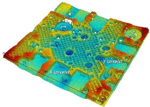
2 Components PCB Side Possible applications include: BGA, LGA, Flip Chip, PoP, QFP, QFN, CSP, TSOP, MLF, etc. Page 2 of 15


![Solder Balls]](/docs-images/89/98085144/images/3-4.jpg "[Solder Ball")
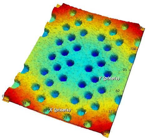
3 - DFP Module Results [Substrate only from BGA with Solder Balls] [Solder Ball Peaks] Page 3 of 15


4 - DIC Module Results Components Top Side [X-Strain Map] Possible applications include: BGA, Flip Chip, Die surface, PoP, Molder surfaces, QFP, TSOP, etc. [PoP: Topside of Bottom Component] [10 x 10 mm Die Surface] Page 4 of 15

5 - DFP Module Results Connectors and Sockets - DFP Module Results Page 5 of 15


6 Wafer Level and Bare Silicon Shields, Heatsinks, and Brake Rotors Page 6 of 15


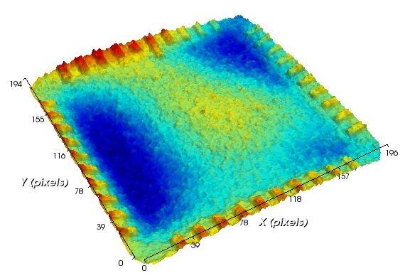
7 PCB Global, Assembled Boards, PCB Cutout Arrays, PCB Locals, Component Strips, Solid State Disks, Memory Devices - DFP Module results Page 7 of 15

8 - DIC Module results Page 8 of 15

9 Other Output Result Formats: Interface Analysis: This software exists as a separate entity from the Studio software. The purpose of Interface Analysis is to allow high-level and in-depth review of the attachment interface between two surfaces that warp during the reflow process. Using Interface Analysis, you can check both Macro characteristics of the interface such as Maximum Gap for all surfaces across all temperatures, and micro details such as the predicted gap between a single interconnect location, at a particular temperature. Page 9 of 15
 Custom Chord Plots: User defined chord plots.")

10 3D Contour Plots: An overhead contour map of 3D surface data (below) Pre-defined Chord Plots: Includes diagonals, edges, and centerline line plots (above) Custom Chord Plots: User defined chord plots. Specific line plots are drawn on an image of the part and plotted as lines (below) Displacement Matrices: A matrix of values where the height is shown in each pixel value and in-plane location is shown by cell location in the matrix. Page 10 of 15
11 Relative Plots: Akrometrix has the ability to take two data sets of the same size, subtract them from one another, and graph (visually or through displacement matrices) these results. This is particularly useful when comparing BGA bottoms to local PCB areas, top and bottom PoP packages, the same part at various temperature, or smoothed/fit data versus raw data (below). [Sample at Room Temperature] [Sample at 220 C] [Relative plot of change between room temperature and 220 C] Page 11 of 15
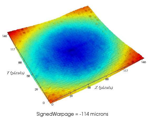
12 Gauges: Coplanarity Coplanarity is the difference between the highest and lowest data points within the Region of Interest. It is always positive. Center Deflection Center Deflection is an Akrometrix specific function defined as the difference between the average height of the four corners and the height at the center: Signed Warpage Signed Warpage has a magnitude equal to the coplanarity, and a sign (or polarity) determined by a special algorithm to distinguish between convex and concave curvature of the surface. The current implementation uses the curvature of the diagonals AB and CD in Figure 1, where the endpoints of the diagonals are adjusted to zero and the sign of the Signed Warpage Gauge is the same as the sign of Equation 1. (1) Figure 1. Coordinate Definitions for Gauges Full-field Signed Warpage Full-field Signed Warpage has a magnitude equal to the coplanarity, and a sign (or polarity) determined by a special algorithm to distinguish between convex and concave curvature of the surface. First, the full surface displacement data is fit to a 2 nd order polynomial. Then the polarity is assigned according to the sign of (, the curvature of the surface along the X and Y axes. Radius of Curvature (ROC) The ROC (Radius of Curvature) gauge returns the radius of a sphere used to fit a three-dimensional surface. A positive ROC sign represents a convex curvature (viewed from above) and a negative sign represents concave curvature. The sign definition is in accordance with JEDEC Standard No. 22B112. Radius of Curvature gauge units are always meters. To calculate the ROC, the 3D surface is first fitted with a sphere using the least squares algorithm. The function of the sphere can be expressed as, where is the sphere center and is the sphere radius. In this sphere function, we define a constraint as follows:, which requires that the sample surface should not be warped more than a semi-sphere shape. Page 12 of 15
13 The ROC gauge is designed for use with a near-sphere-segment shaped surface where there is only one surface curvature center and all four corners are warped in the same direction. The result will be less accurate shapes that do not meet these criteria such as saddle, cylinder, or asymmetric, nearly flat surfaces. Twist According to the IPC-TM-650 Test Methods manual, twist is a measure of the skewness of the opposite edges of a PCB, or equivalently, the extent to which one corner of the PCB lies above or below the plane defined by the other three corners. For a given ROI, Twist is calculated as: (2) where = physical distance of or based on user specified phase image dimensions Units are scaled such that the result is unit less and reported as a percentage. Bow According to the IPC-TM-650 Test Methods manual, bow is a measure of the curvature of the sample along its edges. Bow is reported to be the maximum bow calculated at any point along the four edges of the ROI. The bow value at any edge point along the ROI is determined by: bow (3) where is the displacement measured relative to a chord connecting the edge endpoints and is the edge length based on user specified phase image dimensions. Units are scaled such that the result is unit less and reported as a percentage. Figure 2. Parameter Definitions for Bow Page 13 of 15


14 Measurement Result Applications: Failure Analysis: Many customers use Akrometrix tools when they are seeing a specific problem that may be related to warpage. A common example would be a solder ball crack or open that is found through quality inspection after the reflow process. The warpage data from Akrometrix can often be correlated with failing part types, in locations when warpage is high and/or does not match between solder ball mating surfaces. Warpage or strain data can also correlate to other problems found in packages, including: die cracking, open/cracked leads, and surface delamination. Quality Assurance/Reliability: The TherMoire and LineMoire tools can quantify warpage criteria for customer products. Real world observation of product failures in either outgoing functionality tests or 1-year warranty replacements can be correlated with measured warpage values to find if product failures are specific to warpage levels. High Volume Testing (HVT): New technology introduced to the Studio software in 2011 allows the automatic locating and cropping of multiple samples within the measurement area. This feature, called Part Tracking, is built in to the measurement acquisition software (Surface Measurement). This approach is ideal for the measurement throughput necessary for lot sampling under thermal characterization, for customers doing high volume testing. Pass/Fail decisions versus industry standards: Both JEDEC and JEITA have set industry standards for package warpage. Akrometrix can provide exactly what a customer needs to compare their package with these standards. In fact, many of the example result plots in both of these standards were generated by Akrometrix equipment. Page 14 of 15
15 Matching and comparing shape of package and local site on PCB: Often the most important information can be, not how much a package warps, but how much does it warp in comparison to its mounting surface. Industry standards for package warpage do not take into account the local site warpage of the PCB attachment area. Akrometrix can quantify and compare both surfaces to best understand where package and PCB shape are mismatched. Refer to the section on Interface Analysis. Specific problems observed include: - Die-Substrate delamination - PCB-BGA cold joint/bridging - Stacked Die delamination - Head in Pillow and Head on Pillow defects Material and Design Choices for like Form Factors: Another common design consideration where Akrometrix data can be helpful is in choosing between different materials or designs for the same form factor. A customer may see no difference between three prototypes until they use an Akrometrix system to see which prototype shows favorable warpage characteristics; engineers can then make choices that will lead to more reliable solder joints. The same decisions can also be aided with CTE calculations and strain maps found with the DIC add-on module. Characterization of Local Features: Particularly with the DFP module for larger steps heights, Akrometrix can measure associated heights and consistency of these heights on local features. The ability to draw 2D chord plots is often helpful in these cases. Examples include: - Solder ball height - Solder mask versus bond pad height - Solder mask versus metal trace height - Flatness between connector leads - Socket pin flatness FEA Model Validation: Many companies will predict sample warpage under thermal conditions using FEA modeling software. Actual surface data from a sample through reflow in Akrometrix systems is often used to validate the results of these models. In these cases, Displacement Matrices are particularly useful as they can be imported into many FEA programs. Page 15 of 15
Introduction to High Volume Testing with Part Tracking in Akrometrix Studio 6.0
 Introduction to High Volume Testing with Part Tracking in Akrometrix Studio 6.0 (Twenty sockets automatically located and partitioned in Akrometrix Studio with Part Tracking ) Imagine never partitioning
Improvements in Decision Making Criteria for Thermal Warpage*
 Improvements in Decision Making Criteria for Thermal Warpage* Neil Hubble Director of Engineering *Originally published in imaps Device Packaging 2016 Thermal Warpage & Strain Metrology Concept Overview
Improvements in Decision Making Criteria for Thermal Warpage*
 Improvements in Decision Making Criteria for Thermal Warpage* Neil Hubble Director of Engineering *Originally published in imaps Device Packaging 2016 Thermal Warpage & Strain Metrology Concept Overview
Improvements in Decision Making Criteria for Thermal Warpage*
 Improvements in Decision Making Criteria for Thermal Warpage* Neil Hubble Akrometrix, LLC Atlanta, GA. USA nhubble@akrometrix.com ABSTRACT Surface mount components are commonly evaluated for outof-plane
COMPARING SHADOW MOIRÉ AND DIGITAL FRINGE PROJECTION WARPAGE METROLOGY TECHNIQUES
 COMPARING SHADOW MOIRÉ AND DIGITAL FRINGE PROJECTION WARPAGE METROLOGY TECHNIQUES Neil Hubble Akrometrix Atlanta, GA, USA nhubble@akrometrix.com Leon Weaver Akrometrix Atlanta, GA, USA ABSTRACT Shadow
Survey of Circuit Board Warpage During Reflow
 Survey of Circuit Board Warpage During Reflow Michael J. Varnau Delphi Electronics & Safety 8/20/07 Table of Contents Overview of Goals & Objectives Overview of uct Initial Circuit Board Characterization
ksa MOS Ultra-Scan Performance Test Data
 ksa MOS Ultra-Scan Performance Test Data Introduction: ksa MOS Ultra Scan 200mm Patterned Silicon Wafers The ksa MOS Ultra Scan is a flexible, highresolution scanning curvature and tilt-measurement system.
New Opportunities for 3D SPI
 New Opportunities for 3D SPI Jean-Marc PEALLAT Vi Technology St Egrève, France jmpeallat@vitechnology.com Abstract For some years many process engineers and quality managers have been questioning the benefits
Comparative Analysis of BGA Deformations and Strains Using Digital Image Correlation and Moiré Interferometry
 Comparative Analysis of BGA Deformations and Strains Using Digital Image Correlation and Moiré Interferometry Seungbae Park, Ramji Dhakal and Rahul Joshi Mechanical Engineering Department Binghamton University
Reliability Study of Bottom Terminated Components
 Reliability Study of Bottom Terminated Components Jennifer Nguyen, Hector Marin, David Geiger, Anwar Mohammed, and Murad Kurwa Flextronics International 847 Gibraltar Drive Milpitas, CA, USA Abstract Bottom
Vi Technology 3D Solder Paste Inspection Solutions
 VER.3.0.0 MAR 2008 Vi Technology 3D Solder Paste Inspection Solutions New Opportunities for Solder Paste Inspection Demands of 3D SPI Smaller and finer-pitch components like 01005 and flip-chip Higher
Measurement of Thermally Induced Warpage of BGA Packages/Substrates Using Phase-Stepping Shadow Moiré
 ABSTRACT Measurement of Thermally Induced Warpage of BGA Packages/Substrates Using Phase-Stepping Shadow Moiré Yinyan Wang and Patrick Hassell Electronic Packaging Services, Ltd. Co. 430 Tenth Street,
EFFECT OF PACKAGE WARPAGE AND COMPOSITE CTE ON FAILURE MODES IN BOARD-LEVEL THERMAL CYCLING
 EFFECT OF PACKAGE WARPAGE AND COMPOSITE CTE ON FAILURE MODES IN BOARD-LEVEL THERMAL CYCLING Andrew Mawer, Paul Galles, Mollie Benson and Burt Carpenter NXP Semiconductors, Austin, Texas USA andrew.mawer@nxp.com
Application Note 5363
 Surface Laminar Circuit (SLC) Ball Grid Array (BGA) Lead-free Surface Mount Assembly Application Note 5363 Introduction This document outlines the design and assembly guidelines for surface laminar circuitry
Design and Assembly Process Implementation for BGAs
 ASSOCIATION CONNECTING ELECTRONICS INDUSTRIES Design and Assembly Process Implementation for BGAs Developed by the Device Manufacturers Interface Committee of IPC October 25, 2000 Users of this standard
1. Summary of configurations for end face geometry and measurement conditions. Configurations for End Face Geometry
 31 October 2003 Guidance Document Guidance for Interferometer Inspection of Fiber Optic Ferrule, Fiber End Face Measurements, Ferrules with Domed End Faces 1. Summary of configurations for end face geometry
3D & Advanced Packaging
 Tuesday, October 03, 2017 Company Overview March 12, 2015 3D & ADVANCED PACKAGING IS NOW WITHIN REACH WHAT IS NEXT LEVEL INTEGRATION? Next Level Integration blends high density packaging with advanced
MULTI-FACETED APPROACH TO MINIMIZE PRINTED CIRCUIT BOARD WARPAGE IN BOARD ASSEMBLY PROCESS
 As originally published in the SMTA Proceedings MULTI-FACETED APPROACH TO MINIMIZE PRINTED CIRCUIT BOARD WARPAGE IN BOARD ASSEMBLY PROCESS Srinivasa Aravamudhan, Christopher Combs, Abhishek Prasad, and
Over 5,000 products High Performance Adapters and Sockets Many Custom Designs Engineering Electrical and Mechanical ISO9001:2008 Registration
 Overview Company Overview Over 5,000 products High Performance Adapters and Sockets Many Custom Designs Engineering Electrical and Mechanical ISO9001:2008 Registration Adapter Technology Overview Pluggable
Krzysztof Dabrowiecki, Probe2000 Inc Southwest Test Conference, San Diego, CA June 08, 2004
 Structural stability of shelf probe cards Krzysztof Dabrowiecki, Probe2000 Inc Southwest Test Conference, San Diego, CA June 08, 2004 Presentation Outline Introduction Objectives Multi die applications
E-tec Socketing solutions for BGA, LGA, CGA, CSP, MLF & Gullwing chips
 E-tec Socketing solutions for BGA, LGA, CGA, CSP, MLF & Gullwing chips Available contact styles: Elastomer interposers (10 Ghz & more) Probe pin sockets (generally below 5 Ghz) Other interposer styles
Adapter Technologies
 Adapter Technologies Toll Free: (800) 404-0204 U.S. Only Tel: (952) 229-8200 Fax: (952) 229-8201 email: info@ironwoodelectronics.com Introduction Company Overview Over 5,000 products High Performance Adapters
Patented socketing system for the BGA/CSP technology
 Patented socketing system for the BGA/CSP technology Features: ZIF handling & only 40 grams per contact after closing the socket Sockets adapt to all package styles (at present down to 0.40mm pitch): Ceramic
Flatness Measurement of a Moving Object Using Shadow Moiré Technique with Phase Shifting
 Flatness Measurement of a Moving Object Using Shadow Moiré Technique with Phase Shifting Jiahui Pan, Dirk Zwemer, Gregory Petriccione, and Sean McCarron AkroMetrix, LLC, 700 NE Expy., C-100, Atlanta, GA,
LEADLESS FLIP CHIP PLGA FOR NETWORKING APPLICATIONS
 As originally published in the SMTA Proceedings LEADLESS FLIP CHIP PLGA FOR NETWORKING APPLICATIONS Andrew Mawer, Tara Assi, Steve Safai and Trent Uehling NXP Semiconductors N.V. Austin, TX, USA andrew.mawer@nxp.com
PREDICTIVE AND ANALYTICAL METHODS FOR RAPIDLY ASSESSING THE RELIABILITY OF COMMERCIAL ELECTRONIC PACKAGING FOR MILITARY/INDUSTRIAL ENVIRONMENTS
 PREDICTIVE AND ANALYTICAL METHODS FOR RAPIDLY ASSESSING THE RELIABILITY OF COMMERCIAL ELECTRONIC PACKAGING FOR MILITARY/INDUSTRIAL ENVIRONMENTS S. Rahman, K. K. Choi, T. Zhang, and J. Tang Center for Computer-Aided
Package (1C) Young Won Lim 3/20/13
 Young Won Lim 3/20/13") Copyright (c) 2011-2013 Young W. Lim. Permission is granted to copy, distribute and/or modify this document under the terms of the GNU Free Documentation License, Version 1.2 or any later version published
Copyright (c) 2011-2013 Young W. Lim. Permission is granted to copy, distribute and/or modify this document under the terms of the GNU Free Documentation License, Version 1.2 or any later version published
Laser Technology Inc.
 Laser Shearography Inspection of Helicopter Rotor Blades A helicopter is an aircraft that has a main lifting rotor. Main rotor blades come in a variety of configurations. They can be a hollow composite
Package (1C) Young Won Lim 3/13/13
 Young Won Lim 3/13/13") Copyright (c) 2011-2013 Young W. Lim. Permission is granted to copy, distribute and/or modify this document under the terms of the GNU Free Documentation License, Version 1.2 or any later version published
Copyright (c) 2011-2013 Young W. Lim. Permission is granted to copy, distribute and/or modify this document under the terms of the GNU Free Documentation License, Version 1.2 or any later version published
WARPAGE MEASUREMENT OF PCB USING 3D PROFILOMETRY
 WARPAGE MEASUREMENT OF PCB USING 3D PROFILOMETRY Prepared by Craig Leising 6 Morgan, Ste156, Irvine CA 92618 P: 949.461.9292 F: 949.461.9232 nanovea.com Today's standard for tomorrow's materials. 2010
Correlated Model For Wafer Warpage Prediction of Arbitrarily Patterned Films
 2018 IEEE 68th Electronic Components and Technology Conference Correlated Model For Wafer Warpage Prediction of Arbitrarily Patterned Films Gregory T. Ostrowicki gtostrowicki@ti.com Siva P. Gurum sgurrum@ti.com
Functional Testing of 0.3mm pitch Wafer Level Packages to Multi- GHz Speed made possible by Innovative Socket Technology
 Functional Testing of 0.3mm pitch Wafer Level Packages to Multi- GHz Speed made possible by Innovative Socket Technology Ila Pal - Ironwood Electronics Introduction Today s electronic packages have high
Measurement of Deformation and Strain in Flip Chip on BGA (FC-BGA)
") Measurement of Deformation and Strain in Flip Chip on BGA (FC-BGA) Abstract An autofocus Digital Image Correlation (DIC) workstation incorporating image stacking functionality was used to perform a thermo-mechanical
Measurement of Deformation and Strain in Flip Chip on BGA (FC-BGA) Abstract An autofocus Digital Image Correlation (DIC) workstation incorporating image stacking functionality was used to perform a thermo-mechanical
Wafer Level Packaging The Promise Evolves Dr. Thomas Di Stefano Centipede Systems, Inc. IWLPC 2008
 Wafer Level Packaging The Promise Evolves Dr. Thomas Di Stefano Centipede Systems, Inc. IWLPC 2008 / DEVICE 1.E+03 1.E+02 1.E+01 1.E+00 1.E-01 1.E-02 1.E-03 1.E-04 1.E-05 1.E-06 1.E-07 Productivity Gains
Application Note AN Power QFN Technology Inspection Application Note
 Application Note AN-1137 Power QFN Technology Inspection Application Note Table of Contents Page Inspection techniques... 3 Examples of good assembly... 3 Summary of rejection criteria... 4 Types of faults...
1 INTRODUCTION. Solder paste deposits on grid array of soldering pads. SPI system integration in a PCB assembly production line
 1 INTRODUCTION Test Research Inc. (TRI) designs, manufactures and markets precision test equipment for the world s leading electronics manufacturing service (EMS) companies. Product lines include Automated
Linear, and segmented over up to 1000 points Squareness calibration Matrix compensation over up to 30 x 30 points
 ND 1404 Axes Encoder inputs* 4 (XYZQ)» 1 V PP or «TTL (other interfaces upon request) Subdivision factor* 10-fold (only for 1 V PP ) Display step 1) Display Functions Error compensation Data interface
Socket Technologies
 Socket Technologies Toll Free: (800) 404-0204 U.S. Only Tel: (952) 229-8200 Fax: (952) 229-8201 email: info@ironwoodelectronics.com Introduction Company Overview Over 5,000 products High Performance Adapters
Extract from new. Device Connectivity catalogue. HARTING har-flex. People Power Partnership
 Extract from new Device Connectivity catalogue HARTING har-flex People Power Partnership . har-flex CONNECTORS The continuous scalability by an even number of contacts, i.e. from 6 to 100, of the HARTING
Epigap FAQs Part packges and form factors typical LED packages
 3. packges and form factors 3.1. typical LED packages Radiation from LEDs is generated by a semiconductor chip mounted in a package. LEDs are available in a variety of designs significantly influencing
Measuring Die Tilt Using Shadow Moiré Optical Measurements; New Techniques for Discontinuous and Semi-Reflective Surfaces Phase 2
 Measuring Die Tilt Using Shadow Moiré Optical Measurements; New Techniques for Discontinuous and Semi-Reflective Surfaces Phase 2 Neil Hubble Akrometrix 2700 NE Expressway, Building B500 Atlanta, GA, 30360
And. Modal Analysis. Using. VIC-3D-HS, High Speed 3D Digital Image Correlation System. Indian Institute of Technology New Delhi
 Full Field Displacement And Strain Measurement And Modal Analysis Using VIC-3D-HS, High Speed 3D Digital Image Correlation System At Indian Institute of Technology New Delhi VIC-3D, 3D Digital Image Correlation
Burn-in & Test Socket Workshop
 Burn-in & Test Socket Workshop IEEE March 4-7, 2001 Hilton Mesa Pavilion Hotel Mesa, Arizona IEEE COMPUTER SOCIETY Sponsored By The IEEE Computer Society Test Technology Technical Council COPYRIGHT NOTICE
Eric Lindmark, Ph.D.
 Theory and Practical Application Written by: Eric Lindmark, Ph.D. v061608 4611 Chatsworth Street Shoreview, Minnesota, 55126-5813, USA www.promet.net Introduction In theory, higher bit rate fiber optic
AP Physics: Curved Mirrors and Lenses
 The Ray Model of Light Light often travels in straight lines. We represent light using rays, which are straight lines emanating from an object. This is an idealization, but is very useful for geometric
OPTICAL TOOL FOR IMPACT DAMAGE CHARACTERIZATION ON AIRCRAFT FUSELAGE
 OPTICAL TOOL FOR IMPACT DAMAGE CHARACTERIZATION ON AIRCRAFT FUSELAGE N.Fournier 1 F. Santos 1 - C.Brousset 2 J.L.Arnaud 2 J.A.Quiroga 3 1 NDT EXPERT, 2 AIRBUS France, 3 Universidad Cmplutense de Madrid
Automating Thermal Stress Reflow Simulation on PCBs
 Automating Thermal Stress Reflow Simulation on PCBs Introduction The purpose of this paper is to demonstrate the reflow process of thermal stress reflow simulation on bare PCB s per IPC-TM-650 Test Method
Innovative 3D Structures Utilizing Wafer Level Fan-Out Technology
 Innovative 3D Structures Utilizing Wafer Level Fan-Out Technology JinYoung Khim #, Curtis Zwenger *, YoonJoo Khim #, SeWoong Cha #, SeungJae Lee #, JinHan Kim # # Amkor Technology Korea 280-8, 2-ga, Sungsu-dong,
Custom Connectors Overview
 Company Overview March 12, 2015 Custom Connectors Overview Tuesday, October 03, 2017 CONNECTOR OVERVIEW Engineering Manufacturing Connector Products HiLo FlexFrame Custom Connectors Standard Connectors
Measurement and Prediction of Reliability for Double-Sided Area Array Assemblies
 Measurement and Prediction of Reliability for Double-Sided Area Array Assemblies Anthony Primavera, Ph.D. Mike Meilunas Universal Instruments Corporation Binghamton, NY James M. Pitarresi, Ph.D. Shiva
An integrated solution for KGD: At-speed wafer-level testing and full-contact wafer-level burn-in after flip chip bumping
 An integrated solution for KGD: At-speed wafer-level testing and full-contact wafer-level burn-in after flip chip bumping Yuan-Ping Tseng/ An-Hong Liu TD center ChipMOS Technologies Inc. June 5, 2001 1
Ultra Thin Substrate Assembly Challenges for Advanced Flip Chip Package
 Ultra Thin Substrate Assembly Challenges for Advanced Flip Chip Package by Fred Lee*, Jianjun Li*, Bindu Gurram* Nokibul Islam, Phong Vu, KeonTaek Kang**, HangChul Choi** STATS ChipPAC, Inc. *Broadcom
Advanced BGA Rework Station. Suitable for all kind of reworks on different SMT components
 Advanced BGA Rework Station Suitable for all kind of reworks on different SMT components Advanced BGA Rework Station New Key Features Compact and Stable Design Larger Board Holding Capacity One Touch Lock
Products, Services & Capabilities
 Products, Services & Capabilities Toll Free: (800) 404-0204 U.S. Only Tel: (952) 229-8200 Fax: (952) 229-8201 email: info@ironwoodelectronics.com Overview Company Overview Founded 1986 Over 5,000 products
Space Transformer Performance Study (Final report)
") Space Transformer Performance Study (Final report) Introduction As the pitch of devices becomes smaller, the complexity and cost of the test board becomes significantly higher. In some cases they can no
Space Transformer Performance Study (Final report) Introduction As the pitch of devices becomes smaller, the complexity and cost of the test board becomes significantly higher. In some cases they can no
PROBE CARD METROLOGY
 PROBE CARD METROLOGY HIGH TEMPERATURE TESTING OF PROBE CARDS Rod Schwartz VP & Technical Director Integrated Technology Corporation Dan Kosecki VP Software Development Integrated Technology Corporation
Assembly Considerations for Analog Devices Inc., µmodule TM LGA Packages AUGUST 2018
 Assembly Considerations for Analog Devices Inc., µmodule TM LGA Packages AUGUST 2018 1 Outline Outline Package Construction PCB Design Guidelines Moisture Sensitivity, Pack, Ship & Bake Board Assembly
12X Zoom. Incredible 12X (0.58-7X) magnification for inspection of a wider range of parts.
 magnification for inspection of a wider range of parts.") Incredible 12X (0.58-7X) magnification for inspection of a wider range of parts. Telecentric attachment gives you the world s first parfocal telecentric zoom lens with field coverage up to 50 mm. Increased
Incredible 12X (0.58-7X) magnification for inspection of a wider range of parts. Telecentric attachment gives you the world s first parfocal telecentric zoom lens with field coverage up to 50 mm. Increased
40-Position BGA/LGA PCBeam Connector for Texas Instruments Series 310 DMD
 PCBeam Connector for 40-Position BGA/LGA PCBeam Connector for Texas Instruments Series 310 DMD Neoconix P/N: FBX0040CMFF6AU00 FEATURES High density 0.7424mm area-array pitch Low profile, 1.06mm mated height
Micron Level Placement Accuracy for Wafer Scale Packaging of P-Side Down Lasers in Optoelectronic Products
 Micron Level Placement Accuracy for Wafer Scale Packaging of P-Side Down Lasers in Optoelectronic Products Daniel D. Evans, Jr. and Zeger Bok Palomar Technologies, Inc. 2728 Loker Avenue West Carlsbad,
Stereo Vision Based Automated Solder Ball Height Detection
 Stereo Vision Based Automated Solder Ball Height Detection Jinjin Li 1, Bonnie L. Bennett 2, Lina J. Karam 1, and Jeff S. Pettinato 2 1 School of Electrical, Computer, & Energy Engineering, Arizona State
Solder Reflow Guide for Surface Mount Devices Technical Note
 Solder Reflow Guide for Surface Mount Devices FPGA-TN-02041 Version 3.8 November 2017 Contents Acronyms in This Document... 3 1. Introduction... 4 2. Reflow... 4 3. Inspection... 4 4. Cleaning Recommendations...
Addressing High Precision Automated Optical Inspection Challenges with Unique 3D Technology Solution
 Addressing High Precision Automated Optical Inspection Challenges with Unique 3D Technology Solution John Hoffman CyberOptics Corporation jhoffman@cyberoptics.com Outline/Agenda Phase Profilometry SMT
ASSEMBLY YIELD MODEL FOR AREA ARRAY PACKAGES
 ASSEMBLY YIELD MODEL FOR AREA ARRAY PACKAGES SanJay Sharma Thesis submitted to the faculty of the Virginia Polytechnic Institute and State University in partial fulfillment of the requirements for the
TRIBOMETERS MICRO-MACRO TRIBOLOGY TESTING
 TRIBOMETERS MICRO-MACRO TRIBOLOGY TESTING The Tribometer provides highly accurate and repeatable wear friction testing in rotative and linear modes compliant to ISO and ASTM standards. Designed, at the
Packaging Technology for Image-Processing LSI
 Packaging Technology for Image-Processing LSI Yoshiyuki Yoneda Kouichi Nakamura The main function of a semiconductor package is to reliably transmit electric signals from minute electrode pads formed on
Additional Slides for Lecture 17. EE 271 Lecture 17
 Additional Slides for Lecture 17 Advantages/Disadvantages of Wire Bonding Pros Cost: cheapest packages use wire bonding Allows ready access to front side of die for probing Cons Relatively high inductance
Socket Technologies
 Socket Technologies Introduction Company Overview Over 5,000 products High Performance Adapters and Sockets Many Custom Designs Engineering Electrical and Mechanical ISO9001:2008 Registration Socket Technology
Modularized & parametric modeling methodology.
 Modularized & parametric modeling methodology. Active Device Passive Device Vias Foot print Lid Wall floor PWB Ceramic Taxonomy Technique Mechanical Component Library Analysis model Thermal Structural
Lumaxis, Sunset Hills Rd., Ste. 106, Reston, VA 20190
 White Paper High Performance Projection Engines for 3D Metrology Systems www.lumaxis.net Lumaxis, 11495 Sunset Hills Rd., Ste. 106, Reston, VA 20190 Introduction 3D optical metrology using structured light
Optilia Instruments. Empowering Your Vision!
 Optilia Instruments Empowering Your Vision! Product Review: Optilia BGA Inspection Systems Cutting edge technology in optical inspection of BGA, µbga, CSP and FlipChip soldering! RevB, November-2013 Optical
LGA vs. BGA: WHAT IS MORE RELIABLE? A2 nd LEVEL RELIABILITY COMPARISON
 LGA vs. BGA: WHAT IS MORE RELIABLE? A2 nd LEVEL RELIABILITY COMPARISON Ahmer Syed and Robert Darveaux Amkor Technology 1900 S. Price Road Chandler, AZ 85226 (480)821-5000 asyed@amkor.com ABSTRACT A recent
Using three-dimensional CURVIC contact models to predict stress concentration effects in an axisymmetric model
 Boundary Elements XXVII 245 Using three-dimensional CURVIC contact models to predict stress concentration effects in an axisymmetric model J. J. Rencis & S. R. Pisani Department of Mechanical Engineering,
Coherent Gradient Sensing Microscopy: Microinterferometric Technique. for Quantitative Cell Detection
 Coherent Gradient Sensing Microscopy: Microinterferometric Technique for Quantitative Cell Detection Proceedings of the SEM Annual Conference June 7-10, 010 Indianapolis, Indiana USA 010 Society for Experimental
TROI SPI Series. Key Features Overview
 TROI SPI Series Key Features Overview Key Features Enhanced Color 3D Display Reliable Simultaneous 2D & 3D for Shadow Free Golden Finger Ease of Use Fast & Accurate Strong Sales & Support Network Advanced
The VIC-3D 8 Measurement System
 The VIC-3D 8 Measurement System The VIC-3D 8 system is a turn-key non-contact measurement system for full-field surface shape, deformation, strain, vibration, and much more. The system s core is the VIC-3D
Calibration of a portable interferometer for fiber optic connector endface measurements
 Calibration of a portable interferometer for fiber optic connector endface measurements E. Lindmark Ph.D Light Source Reference Mirror Beamsplitter Camera Calibrated parameters Interferometer Interferometer
3DPIXA: options and challenges with wirebond inspection. Whitepaper
 3DPIXA: options and challenges with wirebond inspection Whitepaper Version Author(s) Date R01 Timo Eckhard, Maximilian Klammer 06.09.2017 R02 Timo Eckhard 18.10.2017 Executive Summary: Wirebond inspection
LQFP. Thermal Resistance. Body Size (mm) Pkg. 32 ld 7 x 7 5 x ld 7 x 7 5 x ld 14 x 14 8 x ld 20 x x 8.5
 Pkg. 32 ld 7 x 7 5 x ld 7 x 7 5 x ld 14 x 14 8 x ld 20 x x 8.5") LQFP Low Profile Quad Flat Pack Packages (LQFP) Amkor offers a broad line of LQFP IC packages designed to provide the same great benefits as MQFP packaging with a 1.4 mm body thickness. These packages
LQFP Low Profile Quad Flat Pack Packages (LQFP) Amkor offers a broad line of LQFP IC packages designed to provide the same great benefits as MQFP packaging with a 1.4 mm body thickness. These packages
Application Note AN-289
 BGA 256-pin Routing Application Note AN-289,QWURGXFWLRQ By Paul Snell and John Afonasiev IDT uses the 256 PBGA package for several of its products. Although creating an optimal layout with a PBGA package
QUALITY ASSURANCE OF MULTIFIBER CONNECTORS
 QUALITY ASSURANCE OF MULTIFIBER CONNECTORS Eric A. Norland/ Daniel Beerbohm Norland Products Inc. Cranbury, NJ 08512 ABSTRACT Industry requirements for compact, high fiber count connectors in both telecom
Advanced Stamping Manufacturing Engineering, Auburn Hills, MI
 RECENT DEVELOPMENT FOR SURFACE DISTORTION MEASUREMENT L.X. Yang 1, C.Q. Du 2 and F. L. Cheng 2 1 Dep. of Mechanical Engineering, Oakland University, Rochester, MI 2 DaimlerChrysler Corporation, Advanced
TB-2026 PROCESS FOR INSTALLATION OF PRESS FIT VHDM BACKPLANE CONNECTORS. Revision G
 PROCESS FOR INSTALLATION OF PRESS FIT VHDM BACKPLANE CONNECTORS Specification Revision Status Revision SCR No. Description Initial Date - 21120 Initial Release D. Manning 3-27-97 A 26393 Revised in its
Release Notes Version 5
 Release Notes Version 5 Version 5.1 (2017-01-31) Solder Joint Fatigue Calculix Support for Column Grid Array (CGA) modeling for Solder Joint Fatigue FEA analysis and the Solder Fatigue tool has been added
GDL Toolbox 2 Reference Manual
 Reference Manual Archi-data Ltd. Copyright 2002. New Features Reference Manual New Save GDL command Selected GDL Toolbox elements can be exported into simple GDL scripts. During the export process, the
Application Note AN-1703 Strain Filter Selection
 Application Note AN-1703 Strain Filter Selection Introduction Strain filters in Vic-2D and Vic-3D are user-defined so that users can select how localized or how averaged the strains will be presented in
Miniature 2.4 GHz Vertical-Mount PCBA Antenna
 Miniature 2.4 GHz Vertical-Mount PCBA Antenna Product Description Parsec s PTA2.4-V is a miniature 2.4 GHz antenna for Bluetooth, ZigBee, and Wi-Fi with 6.4 x 15.05 x 0.15 mm ( H x W x thickness) dimensions.
IT3D(M)-300S-BGA (37) Lead-Free THERMAL CYCLING TEST REPORT
-300S-BGA (37) Lead-Free THERMAL CYCLING TEST REPORT") TR066E-018 ITD(M)-00S-BGA (7) Lead-Free THERMAL CYCLING TEST REPORT - Post 6000 Cycles Report - APPROVED TY.ARAI Nov. 18, 009 CHECKED TM.MATSUO Nov. 17, 009 CHARGED TY.TAKADA Nov. 17, 009 HIROSE ELECTRIC
TR066E-018 ITD(M)-00S-BGA (7) Lead-Free THERMAL CYCLING TEST REPORT - Post 6000 Cycles Report - APPROVED TY.ARAI Nov. 18, 009 CHECKED TM.MATSUO Nov. 17, 009 CHARGED TY.TAKADA Nov. 17, 009 HIROSE ELECTRIC
Minimizing Noise and Bias in 3D DIC. Correlated Solutions, Inc.
 Minimizing Noise and Bias in 3D DIC Correlated Solutions, Inc. Overview Overview of Noise and Bias Digital Image Correlation Background/Tracking Function Minimizing Noise Focus Contrast/Lighting Glare
3-D Package Integration Enabling Technologies
 3-D Package Integration Enabling Technologies Nanium - Semi Networking Day David Clark - Choon Heung Lee - Ron Huemoeller June 27th, 2013 Enabling a Microelectronic World Mobile Communications Driving
Vincotech's Compliant Pin. Application Note. Advantages of Vincotech's Power Modules with Press-fit Technology
 Application Note Vincotech's Compliant Pin Advantages of Vincotech's Power Modules with Press-fit Technology Application Note no.: AN_2010-10_001-v04 Table of Contents Revision history:... 3 1 Abstract...
Thermo Mechanical Modeling of TSVs
 Thermo Mechanical Modeling of TSVs Jared Harvest Vamsi Krishna ih Yaddanapudi di 1 Overview Introduction to Through Silicon Vias (TSVs) Advantages of TSVs over wire bonding in packages Role of TSVs in
Chapter 1 Introduction of Electronic Packaging
 Chapter 1 Introduction of Electronic Packaging 1 Introduction of Electronic Packaging 2 Why Need Package? IC Foundry Packaging house Module Sub-system Product 3 Concept of Electric Packaging 4 Moore s
PROCESSING RECOMMENDATIONS
 PROCESSING RECOMMENDATIONS For Samtec s 0.80mm SEARAY Right Angle (SEAF8-RA) Connectors The method used to solder these high-density connectors is the same as that used for many BGA devices even though
Lecture 3 Sections 2.2, 4.4. Mon, Aug 31, 2009
 Model s Lecture 3 Sections 2.2, 4.4 World s Eye s Clip s s s Window s Hampden-Sydney College Mon, Aug 31, 2009 Outline Model s World s Eye s Clip s s s Window s 1 2 3 Model s World s Eye s Clip s s s Window
Challenges of Integration of Complex FHE Systems. Nancy Stoffel GE Global Research
 Challenges of Integration of Complex FHE Systems Nancy Stoffel GE Global Research Products drive requirements to sub-systems, components and electronics GE PRODUCTS CTQs: SWaP, $$, operating environment,
Mathematics High School Geometry An understanding of the attributes and relationships of geometric objects can be applied in diverse contexts
 Mathematics High School Geometry An understanding of the attributes and relationships of geometric objects can be applied in diverse contexts interpreting a schematic drawing, estimating the amount of
Advanced Vision Guided Robotics. David Bruce Engineering Manager FANUC America Corporation
 Advanced Vision Guided Robotics David Bruce Engineering Manager FANUC America Corporation Traditional Vision vs. Vision based Robot Guidance Traditional Machine Vision Determine if a product passes or
IC Obsolescence Solutions
 Company Overview March 12, 2015 Tuesday, October 03, 2017 IC FOOTPRINT CONVERSION ADAPTERS REPLACE OBSOLETE ICs WITHOUT RE-SPINNING YOUR PCB An IC Adapter is a small PCB designed that: Has a circuit and