Challenges of Integration of Complex FHE Systems. Nancy Stoffel GE Global Research
|
|
|
- Magnus McGee
- 5 years ago
- Views:
Transcription

1 Challenges of Integration of Complex FHE Systems Nancy Stoffel GE Global Research


2 Products drive requirements to sub-systems, components and electronics GE PRODUCTS CTQs: SWaP, $$, operating environment, life SYSTEMS & COMPONENTS CTQs: Efficiency, Torque, life, operating environment, stresses, etc. PACKAGING TECHNOLOGY CTQs: Size, power, communication, Heat Flux Density

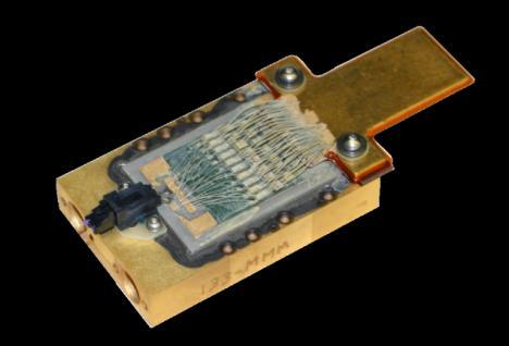
3 Flexible Hybrid Electronics Devices CMOS, MEMS, InP, GaAs, SiC Flexible Substrate New Materials & Processes Low cost Mfg methods FHE microsystem integration methods New Products Existing Products: New functionality via form factor, robustness etc New types of products

4 Interest in Wearables for Health Care From ICU to General Ward to Homecare 1. Traditional vital sign From monitoring: ICU to General Ward to H Wirefree Reduce cost and footprint o Comfort wearable devices- disposa Disposable 2. Implement New patient monitoring and develop ne parameters- sensors hydration Patient Experience Drives Requirements for : Wirefree monitoring Comfort on skin Reliable monitoring Comfortable form factor Disposable for infection control Battery, power management, RF communication, antenna, communication infrastructure in hospital or other setting New substrates: soft Robust sensor connection to patient, Data communication rates, signal fidelity, robust signal processing Miniaturization, thin devices or device packages, body attachment methods Low cost mfg methods, materials choices, product life cycle studies, Regulatory issues


5 FHE Elements for Monitoring System Sense Mechanical Thermal chemical Biological Opticalelectrical Power Process Signal Processing A/D Memory Communicat e Wireless Near Field User Display


6 Promise of Asset Monitoring Condition based monitoring of machine or structure to gain max productivity, performance and safety Requirements: Low profile on structure so as not to interfere with function Robust Attachment techniques to machine, tool or asset Energy Management: may require remote power sources Will be relatively low volume products Many applications are in harsh environments, and will require higher temperature sensor, substrates and interconnects
 Thin Device Handling: Pick and Place Electrical Interconnect Encapsulation Flexible Circuit Preparation Integration Flex circuitization Lamination for multilayers Via formation Pad")
7 Simple Process Flow for Chip on Flex Based Flexible Hybrid Electronics Device Wafer UBM or Redistribution Layer Routing Device Preparation Wafer Thinning (optional) Device Singulation Packaging of device (optional) Thin Device Handling: Pick and Place Electrical Interconnect Encapsulation Flexible Circuit Preparation Integration Flex circuitization Lamination for multilayers Via formation Pad finish Challenges: Maximum Form Factor Reduction Requires Change in Packaging Approach to Chip Scale Package or Thin Bare Die New materials/methods for flex circuits are not compatible with standard methods of die attach/interconnect (thermal & surface finish) Dynamic flexing, chip on flex prone to die delamination and die cracking. CTE mismatch between substrate and film Some Substrates of interest for wearables lack dimensional stability Modification of methods will be necessary to meet all CTQs
8 1 3M ACF GaTech-PRC on rigid interposer 3-StatsChip Pac 4- i3 Integration done on PI 5-GE POL techno 6-Ormet Tech Overview May 2012 Interconnect method Make table Interconnections: new approaches Low T compatible (<150C) Die position Bond pad prep I/O PItch Flip Chip BGA No facedown Yes, RDL and solderable finsh Copper pillar thermocompression No facedown Solder tipped copper pillar Copper bumps/ pillars into NCP No facedown Solder tipped copper pillar Area Array mm micro BGA: mm Area array 20 um 2 70 um 4 on flex Area array 40/80 um 3 Anisotropic conductive adhesive Yes facedown Bump Area array 200 um 1 Printed Interconnect yes up No Perimeter 100 um Micro via direct plated connections yes facedown no Area Array 50 um 5 3D Compliant structures Yes facedown Copper cantilevers, springs transient liquid phase sintering adhesives TAB Yes? Up Yes, bondable metal Wire-bonding yes up Yes, bondable metal Area array facedown bump Area array 300 um 6 Perimeter Perimeter 30 um 45 um


9 Integrated Flex System In Package Technology for Wearables, Portable Devices and Power Conversion Miniaturization of Advanced packaging technology ideal for industrial & consumer electronics as well as high power and RF applications. Integration of Sensors, Microprocessors, Antenna, Passives on single or multilayer flex platform High-Capability & High-Reliability technology with proven performance under exceptional environments Unique flex-based interconnection technology forms a foundation for the high quality, high volume production process
10 GE Thin Profile POL Development Objective to extend POL technology to thin profile packages for FOWLP, SiP, and PoP applications. Focus on sub 200µm modules with conductor layers on one or both sides. Structure realized using thin (~50µm) die and 25 µm PI layers. Early test vehicles and reliability testing done. Current development focused on manufacturability and handling of thin modules as well as full package qualification.

11 Balanced core structure with equal material layers on both side of the module <10 um die warp Thin Profile POL Module target thicknesses (actual ~-4%) Soldermask 20µm Objective to extend POL technology to 12µm thin profile packages for FOWLP, SiP, 23µm and PoP applications. Adhesive 13µm Focus on sub 200µm modules with conductor layers on one or both sides. Die PI 50µm Structure realized using thin (~50µm) die and 25 µm PI layers. 13µm Early test vehicles PI and reliability 23µm testing done. Cu 12µm 20µm 186µm Current development focused on manufacturability and handling of thin modules as well as full package qualification.
12 Conclusions Development of FHE infrastructure offers opportunities for new product implementations Products will require integration of sensing, computing, communication Manufacturing materials, processes, infrastructure, reliability needs to be addressed within Next Flex Program.
Bringing 3D Integration to Packaging Mainstream
 Bringing 3D Integration to Packaging Mainstream Enabling a Microelectronic World MEPTEC Nov 2012 Choon Lee Technology HQ, Amkor Highlighted TSV in Packaging TSMC reveals plan for 3DIC design based on silicon
TechSearch International, Inc.
 Silicon Interposers: Ghost of the Past or a New Opportunity? Linda C. Matthew TechSearch International, Inc. www.techsearchinc.com Outline History of Silicon Carriers Thin film on silicon examples Multichip
Advanced CSP & Turnkey Solutions. Fumio Ohyama Tera Probe, Inc.
 Advanced CSP & Turnkey Solutions Fumio Ohyama Tera Probe, Inc. Tera Probe - Corporate Overview 1. Company : Tera Probe, Inc. 2. Founded : August, 2005 3. Capital : Approx. USD118.2 million (as of March
Packaging Technology for Image-Processing LSI
 Packaging Technology for Image-Processing LSI Yoshiyuki Yoneda Kouichi Nakamura The main function of a semiconductor package is to reliably transmit electric signals from minute electrode pads formed on
Heterogeneous Integration and the Photonics Packaging Roadmap
 Heterogeneous Integration and the Photonics Packaging Roadmap Presented by W. R. Bottoms Packaging Photonics for Speed & Bandwidth The Functions Of A Package Protect the contents from damage Mechanical
New Era of Panel Based Technology for Packaging, and Potential of Glass. Shin Takahashi Technology Development General Division Electronics Company
 New Era of Panel Based Technology for Packaging, and Potential of Glass Shin Takahashi Technology Development General Division Electronics Company Connecting the World Connecting the World Smart Mobility
SMAFTI Package Technology Features Wide-Band and Large-Capacity Memory
 SMAFTI Package Technology Features Wide-Band and Large-Capacity Memory KURITA Yoichiro, SOEJIMA Koji, KAWANO Masaya Abstract and NEC Corporation have jointly developed an ultra-compact system-in-package
Embedded UTCP interposers for miniature smart sensors
 Embedded UTCP interposers for miniature smart sensors T. Sterken 1,2, M. Op de Beeck 2, Tom Torfs 2, F. Vermeiren 1,2, C. Van Hoof 2, J. Vanfleteren 1,2 1 CMST (affiliated with Ugent and IMEC), Technologiepark
Packaging Challenges for High Performance Mixed Signal Products. Caroline Beelen-Hendrikx, Eef Bagerman Semi Networking Day Porto, June 27, 2013
 Packaging Challenges for High Performance Mixed Signal Products Caroline Beelen-Hendrikx, Eef Bagerman Semi Networking Day Porto, June 27, 2013 Content HPMS introduction Assembly technology drivers for
Packaging of Selected Advanced Logic in 2x and 1x nodes. 1 I TechInsights
 Packaging of Selected Advanced Logic in 2x and 1x nodes 1 I TechInsights Logic: LOGIC: Packaging of Selected Advanced Devices in 2x and 1x nodes Xilinx-Kintex 7XC 7 XC7K325T TSMC 28 nm HPL HKMG planar
3D technology for Advanced Medical Devices Applications
 3D technology for Advanced Medical Devices Applications By, Dr Pascal Couderc,Jerome Noiray, Dr Christian Val, Dr Nadia Boulay IMAPS MEDICAL WORKSHOP DECEMBER 4 & 5,2012 P.COUDERC 3D technology for Advanced
Material technology enhances the density and the productivity of the package
 Material technology enhances the density and the productivity of the package May 31, 2018 Toshihisa Nonaka, Ph D. Packaging Solution Center Advanced Performance Materials Business Headquarter Hitachi Chemical
Innovative 3D Structures Utilizing Wafer Level Fan-Out Technology
 Innovative 3D Structures Utilizing Wafer Level Fan-Out Technology JinYoung Khim #, Curtis Zwenger *, YoonJoo Khim #, SeWoong Cha #, SeungJae Lee #, JinHan Kim # # Amkor Technology Korea 280-8, 2-ga, Sungsu-dong,
Solving Integration Challenges for Flexible Hybrid Electronics
 Solving Integration Challenges for Flexible Hybrid Electronics Nano for Defense Conference November 17, 2015 Approved for Public Release What are Flexible Hybrid Electronics? Printed Electronics Low Cost,
Wafer Level Packaging The Promise Evolves Dr. Thomas Di Stefano Centipede Systems, Inc. IWLPC 2008
 Wafer Level Packaging The Promise Evolves Dr. Thomas Di Stefano Centipede Systems, Inc. IWLPC 2008 / DEVICE 1.E+03 1.E+02 1.E+01 1.E+00 1.E-01 1.E-02 1.E-03 1.E-04 1.E-05 1.E-06 1.E-07 Productivity Gains
3-D Package Integration Enabling Technologies
 3-D Package Integration Enabling Technologies Nanium - Semi Networking Day David Clark - Choon Heung Lee - Ron Huemoeller June 27th, 2013 Enabling a Microelectronic World Mobile Communications Driving
Embedded Power Dies for System-in-Package (SiP)
") Embedded Power Dies for System-in-Package (SiP) D. Manessis, L. Boettcher, S. Karaszkiewicz, R.Patzelt, D. Schuetze, A. Podlasky, A. Ostmann Fraunhofer Institute for Reliability and Microintegration (IZM),
Embedded Power Dies for System-in-Package (SiP) D. Manessis, L. Boettcher, S. Karaszkiewicz, R.Patzelt, D. Schuetze, A. Podlasky, A. Ostmann Fraunhofer Institute for Reliability and Microintegration (IZM),
Power Matters. TM. Why Embedded Die? Piers Tremlett Microsemi 22/9/ Microsemi Corporation. Company Proprietary 1
 Power Matters. TM Why Embedded Die? Piers Tremlett Microsemi 22/9/16 1 Introduction This presentation: Outlines our journey to make miniaturised SiP modules Compares : Embedded Die Technology (EDT) With
From 3D Toolbox to 3D Integration: Examples of Successful 3D Applicative Demonstrators N.Sillon. CEA. All rights reserved
 From 3D Toolbox to 3D Integration: Examples of Successful 3D Applicative Demonstrators N.Sillon Agenda Introduction 2,5D: Silicon Interposer 3DIC: Wide I/O Memory-On-Logic 3D Packaging: X-Ray sensor Conclusion
Comparison & highlight on the last 3D TSV technologies trends Romain Fraux
 Comparison & highlight on the last 3D TSV technologies trends Romain Fraux Advanced Packaging & MEMS Project Manager European 3D Summit 18 20 January, 2016 Outline About System Plus Consulting 2015 3D
Package (1C) Young Won Lim 3/13/13
 Young Won Lim 3/13/13") Copyright (c) 2011-2013 Young W. Lim. Permission is granted to copy, distribute and/or modify this document under the terms of the GNU Free Documentation License, Version 1.2 or any later version published
Copyright (c) 2011-2013 Young W. Lim. Permission is granted to copy, distribute and/or modify this document under the terms of the GNU Free Documentation License, Version 1.2 or any later version published
Multi-Die Packaging How Ready Are We?
 Multi-Die Packaging How Ready Are We? Rich Rice ASE Group April 23 rd, 2015 Agenda ASE Brief Integration Drivers Multi-Chip Packaging 2.5D / 3D / SiP / SiM Design / Co-Design Challenges: an OSAT Perspective
Advances in Flexible Hybrid Electronics Reliability
 Advances in Flexible Hybrid Electronics Reliability LOPEC Smart & Hybrid Systems Munich 3/29/17 This work sponsored in part by Air Force Research Laboratory, Wright-Patterson AFB, for supporting reliability
Collaboration for Breakthrough Innovation in Human Performance Monitoring for the Warfighter
 Collaboration for Breakthrough Innovation in Human Performance Monitoring for the Warfighter NDIA 2018 Human Systems Conference Dr. Melissa Grupen-Shemansky Chief Technology Officer, SEMI / FlexTech megshemansky@semi.org
Rethinking the Hierarchy of Electronic Interconnections. Joseph Fjelstad Verdant Electronics
 Rethinking the Hierarchy of Electronic Interconnections Joseph Fjelstad Verdant Electronics The Industry s Terminology Challenge» The electronics industry continues to explore and develop new methods to
Burn-in & Test Socket Workshop
 Burn-in & Test Socket Workshop IEEE March 4-7, 2001 Hilton Mesa Pavilion Hotel Mesa, Arizona IEEE COMPUTER SOCIETY Sponsored By The IEEE Computer Society Test Technology Technical Council COPYRIGHT NOTICE
Thermo Mechanical Modeling of TSVs
 Thermo Mechanical Modeling of TSVs Jared Harvest Vamsi Krishna ih Yaddanapudi di 1 Overview Introduction to Through Silicon Vias (TSVs) Advantages of TSVs over wire bonding in packages Role of TSVs in
3D & Advanced Packaging
 Tuesday, October 03, 2017 Company Overview March 12, 2015 3D & ADVANCED PACKAGING IS NOW WITHIN REACH WHAT IS NEXT LEVEL INTEGRATION? Next Level Integration blends high density packaging with advanced
FHE Integration & Manufacturing for Killer Apps
 FHE Integration & Manufacturing for Killer Apps Nov. 18, 2015 Doug Hackler Introduction Small Business Privately Held Founded Nov. 2001 Member: New Boise, Idaho Facility Headquarters and manufacturing
Your Microelectronic Package Assembly Solution for MEMS Sensors. SMART Microsystems Ltd.
 Your Microelectronic Package Assembly Solution for MEMS Sensors Why MEMS is Important Growing Industry Segments About SMART Microsystems What We Do How We Do It Working with SMART 2 Why MEMS is Important
High Reliability Electronics for Harsh Environments
 High Reliability Electronics for Harsh Environments Core Capabilities API Technologies is a world leader in the supply of microelectronic products and services supporting mission critical applications,
Package (1C) Young Won Lim 3/20/13
 Young Won Lim 3/20/13") Copyright (c) 2011-2013 Young W. Lim. Permission is granted to copy, distribute and/or modify this document under the terms of the GNU Free Documentation License, Version 1.2 or any later version published
Copyright (c) 2011-2013 Young W. Lim. Permission is granted to copy, distribute and/or modify this document under the terms of the GNU Free Documentation License, Version 1.2 or any later version published
3D Integration & Packaging Challenges with through-silicon-vias (TSV)
") NSF Workshop 2/02/2012 3D Integration & Packaging Challenges with through-silicon-vias (TSV) Dr John U. Knickerbocker IBM - T.J. Watson Research, New York, USA Substrate IBM Research Acknowledgements IBM
NSF Workshop 2/02/2012 3D Integration & Packaging Challenges with through-silicon-vias (TSV) Dr John U. Knickerbocker IBM - T.J. Watson Research, New York, USA Substrate IBM Research Acknowledgements IBM
Solving Integration Challenges for Printed and Flexible Hybrid Electronics
 Solving Integration Challenges for Printed and Flexible Hybrid Electronics SEMICON West 16 July 2015 Proprietary Information www.americansemi.com What are Flexible Hybrid Electronics 2 Flexible Hybrid
Vertical Circuits. Small Footprint Stacked Die Package and HVM Supply Chain Readiness. November 10, Marc Robinson Vertical Circuits, Inc
 Small Footprint Stacked Die Package and HVM Supply Chain Readiness Marc Robinson Vertical Circuits, Inc November 10, 2011 Vertical Circuits Building Blocks for 3D Interconnects Infrastructure Readiness
Non-contact Test at Advanced Process Nodes
 Chris Sellathamby, J. Hintzke, B. Moore, S. Slupsky Scanimetrics Inc. Non-contact Test at Advanced Process Nodes June 8-11, 8 2008 San Diego, CA USA Overview Advanced CMOS nodes are a challenge for wafer
Ultra Thin Substrate Assembly Challenges for Advanced Flip Chip Package
 Ultra Thin Substrate Assembly Challenges for Advanced Flip Chip Package by Fred Lee*, Jianjun Li*, Bindu Gurram* Nokibul Islam, Phong Vu, KeonTaek Kang**, HangChul Choi** STATS ChipPAC, Inc. *Broadcom
Technology Platform and Trend for SiP Substrate. Steve Chiang, Ph.D CSO of Unimicron Technology
 Technology Platform and Trend for SiP Substrate Steve Chiang, Ph.D CSO of Unimicron Technology Contents Unimicron Introduction SiP Evolution Unimicron SiP platform - PCB, RF, Substrate, Glass RDL Connector.
CMOSETR Session C1, July 7 (Macroelectronics)
") Universal Flexible Hybrid System Development Kit including MCU, ADC and RFIC Prepared for: CMOSETR Session C1, July 7 (Macroelectronics) Doug Hackler President & CEO doughackler@americansemi.com 208 336-2773
Universal Flexible Hybrid System Development Kit including MCU, ADC and RFIC Prepared for: CMOSETR Session C1, July 7 (Macroelectronics) Doug Hackler President & CEO doughackler@americansemi.com 208 336-2773
Advanced Packaging for Wearables (Vital Signs Monitoring) Vikram Venkatadri IMAPS New England 5/1/2018
 Vikram Venkatadri IMAPS New England 5/1/2018") Advanced Packaging for Wearables (Vital Signs Monitoring) Vikram Venkatadri IMAPS New England 5/1/2018 Healthcare at ADI Improving Quality of Life Through Better Care Technology Diagnostics & therapy Imaging
Advanced Packaging for Wearables (Vital Signs Monitoring) Vikram Venkatadri IMAPS New England 5/1/2018 Healthcare at ADI Improving Quality of Life Through Better Care Technology Diagnostics & therapy Imaging
Photonics Integration in Si P Platform May 27 th Fiber to the Chip
 Photonics Integration in Si P Platform May 27 th 2014 Fiber to the Chip Overview Introduction & Goal of Silicon Photonics Silicon Photonics Technology Wafer Level Optical Test Integration with Electronics
Advances in FHE Integration using FleXform-ADC. 2016FLEX Conference March 03, 2015
 Advances in FHE Integration using FleXform-ADC 2016FLEX Conference March 03, 2015 What are Flexible Hybrid Electronics? Printed Electronics Low Cost, R2R, Large Format Flexible Hybrid System Combination
Beyond Chip Stacking---Quilt Packaging Enabled 3D Systems
 Beyond Chip Stacking---Quilt Packaging Enabled 3D Systems Jason Kulick, President & Co-Founder jason.kulick@indianaic.com 574-217-4612 (South Bend, IN) May 3, 2016 2016 New England IMAPS Symposium Presentation
Ultra Fine Pitch RDL Development in Multi-layer ewlb (embedded Wafer Level BGA) Packages
 Packages") Ultra Fine Pitch RDL Development in Multi-layer ewlb (embedded Wafer Level BGA) Packages Won Kyoung Choi*, Duk Ju Na*, Kyaw Oo Aung*, Andy Yong*, Jaesik Lee**, Urmi Ray**, Riko Radojcic**, Bernard Adams***
Ultra Fine Pitch RDL Development in Multi-layer ewlb (embedded Wafer Level BGA) Packages Won Kyoung Choi*, Duk Ju Na*, Kyaw Oo Aung*, Andy Yong*, Jaesik Lee**, Urmi Ray**, Riko Radojcic**, Bernard Adams***
ARCHIVE 2008 COPYRIGHT NOTICE
 Keynote Speaker ARCHIVE 2008 Packaging & Assembly in Pursuit of Moore s Law and Beyond Karl Johnson Ph.D. Vice President and Senior Fellow Advanced Packaging Systems Integration Laboratory Freescale Semiconductor
Applications, Processing and Integration Options for High Dielectric Constant Multi-Layer Thin-Film Barium Strontium Titanate (BST) Capacitors
 Capacitors") Applications, Processing and Integration Options for High Dielectric Constant Multi-Layer Thin-Film Barium Strontium Titanate (BST) Capacitors Agenda Introduction What is BST? Unique Characteristics of
Applications, Processing and Integration Options for High Dielectric Constant Multi-Layer Thin-Film Barium Strontium Titanate (BST) Capacitors Agenda Introduction What is BST? Unique Characteristics of
SYSTEM IN PACKAGE AND FUNCTIONAL MODULE FOR MOBILE AND IoT DEVICE ASSEMBLY
 SYSTEM IN PACKAGE AND FUNCTIONAL MODULE FOR MOBILE AND IoT DEVICE ASSEMBLY W. Koh, PhD Huawei Technologies JEDEC Mobile & IOT Forum Copyright 2017 Huawei Technologies, Ltd. OUTLINE Mobile and IoT Device
Advanced Packaging For Mobile and Growth Products
 Advanced Packaging For Mobile and Growth Products Steve Anderson, Senior Director Product and Technology Marketing, STATS ChipPAC Growing Needs for Silicon & Package Integration Packaging Trend Implication
DEPARTMENT WAFER LEVEL SYSTEM INTEGRATION
 FRAUNHOFER INSTITUTE FOR RELIABILITY AND MICROINTEGRATION IZM DEPARTMENT WAFER LEVEL SYSTEM INTEGRATION ALL SILICON SYSTEM INTEGRATION DRESDEN ASSID ALL SILICON SYSTEM INTEGRATION DRESDEN FRAUNHOFER IZM-ASSID
Packaging Innovation for our Application Driven World
 Packaging Innovation for our Application Driven World Rich Rice ASE Group March 14 th, 2018 MEPTEC / IMAPS Luncheon Series 1 What We ll Cover Semiconductor Roadmap Drivers Package Development Thrusts Collaboration
Stacked Silicon Interconnect Technology (SSIT)
") Stacked Silicon Interconnect Technology (SSIT) Suresh Ramalingam Xilinx Inc. MEPTEC, January 12, 2011 Agenda Background and Motivation Stacked Silicon Interconnect Technology Summary Background and Motivation
Stacked Silicon Interconnect Technology (SSIT) Suresh Ramalingam Xilinx Inc. MEPTEC, January 12, 2011 Agenda Background and Motivation Stacked Silicon Interconnect Technology Summary Background and Motivation
TechSearch International, Inc.
 Packaging and Assembly for Wearable Electronics Timothy G. Lenihan, Ph.D. Senior Analyst TechSearch International, Inc. www.techsearchinc.com What s Wearable Electronics? Wearable electronics not clearly
Wafer Probe card solutions
 Wafer Probe card solutions Innovative Solutions to Test Chips in the Semiconductor Industry Our long term experience in the electronic industry and our strong developing and process teams are inspired
ECP Embedded Component Packaging Technology
 ECP Embedded Component Packaging Technology A.Kriechbaum, H.Stahr, M.Biribauer, N.Haslebner, M.Morianz, M.Beesley AT&S Austria Technologie und Systemtechnik AG Abstract The packaging market has undergone
Flexible Hybrid Electronics Solutions for Wearable Sensor Systems. Richard Chaney American Semiconductor, Inc.
 Flexible Hybrid Electronics Solutions for Wearable Sensor Systems Richard Chaney American Semiconductor, Inc. What is a Flexible Hybrid System (FHS)? Printed Electronics Low Cost, R2R, Large Format Flexible
Review of New, Flexible MEMS Technology to Reduce Cost of Test for Multi-site Wire Bond Applications
 Review of New, Flexible MEMS Technology to Reduce Cost of Test for Multi-site Wire Bond Applications Dan Stillman Texas Instruments Ben Eldridge FormFactor Overview Project Background & Objective Probe
Wafer Probe card solutions
 Wafer Probe card solutions Innovative Solutions to Test Chips in the Semiconductor Industry Our long term experience in the electronic industry and our strong developing and process teams are inspired
IMEC CORE CMOS P. MARCHAL
 APPLICATIONS & 3D TECHNOLOGY IMEC CORE CMOS P. MARCHAL OUTLINE What is important to spec 3D technology How to set specs for the different applications - Mobile consumer - Memory - High performance Conclusions
Solving Integration Challenges for Flexible Hybrid Electronics. High performance flexible electronics
 Solving Integration Challenges for Flexible Hybrid Electronics High performance flexible electronics Wearable Sensor System Configurations 2 Wearable Hybrid System Sensor Signal Processing Data Processing
inemi Roadmap and Technical Plan on Organic PCB Bill Bader, inemi inemi PCB/Laminate Workshop, Taipei October 22, 2013
 inemi Roadmap and Technical Plan on Organic PCB Bill Bader, inemi inemi PCB/Laminate Workshop, Taipei October 22, 2013 Agenda inemi Roadmap Process and Scope 2013 PCB Roadmap and TIG Outcomes Summary &
Comparison of Singulation Techniques
 Comparison of Singulation Techniques Electronic Packaging Society, Silicon Valley Chapter Sept. 28, 2017 ANNETTE TENG Sept 28, 2017 1 Definition of Singulation 9/28/2017 Annetteteng@promex-ind.com 2 www.cpmt.org/scv
Physical Design Implementation for 3D IC Methodology and Tools. Dave Noice Vassilios Gerousis
 I NVENTIVE Physical Design Implementation for 3D IC Methodology and Tools Dave Noice Vassilios Gerousis Outline 3D IC Physical components Modeling 3D IC Stack Configuration Physical Design With TSV Summary
MOLEX COPPER FLEXIBLE CIRCUIT SOLUTIONS
 MOLEX COPPER FLEXIBLE CIRCUIT SOLUTIONS CIRCUITS DESIGNED WITH A RANGE OF CAPABILITIES Maximum Performance for Demanding Applications Flex and Rigid Flex (Typical) Layer Count 1 to 8 Layers Standard Panel
TechSearch International, Inc.
 On the Road to 3D ICs: Markets and Solutions E. Jan Vardaman President TechSearch International, Inc. www.techsearchinc.com High future cost of lithography Severe interconnect delay Noted in ITRS roadmap
LQFP. Thermal Resistance. Body Size (mm) Pkg. 32 ld 7 x 7 5 x ld 7 x 7 5 x ld 14 x 14 8 x ld 20 x x 8.5
 Pkg. 32 ld 7 x 7 5 x ld 7 x 7 5 x ld 14 x 14 8 x ld 20 x x 8.5") LQFP Low Profile Quad Flat Pack Packages (LQFP) Amkor offers a broad line of LQFP IC packages designed to provide the same great benefits as MQFP packaging with a 1.4 mm body thickness. These packages
LQFP Low Profile Quad Flat Pack Packages (LQFP) Amkor offers a broad line of LQFP IC packages designed to provide the same great benefits as MQFP packaging with a 1.4 mm body thickness. These packages
TechSearch International, Inc.
 Alternatives on the Road to 3D TSV E. Jan Vardaman President TechSearch International, Inc. www.techsearchinc.com Everyone Wants to Have 3D ICs 3D IC solves interconnect delay problem bandwidth bottleneck
Application Development for Flexible Hybrid Printed Electronics
 Application Development for Flexible Hybrid Printed Electronics Lok Boon Keng, Yusoff Bin Ismail, Joseph Chen Sihan, Cheng Ge, Ronnie Teo Large Area Processing Programme Emerging Application Division Outline
Application Note 5363
 Surface Laminar Circuit (SLC) Ball Grid Array (BGA) Lead-free Surface Mount Assembly Application Note 5363 Introduction This document outlines the design and assembly guidelines for surface laminar circuitry
WLSI Extends Si Processing and Supports Moore s Law. Douglas Yu TSMC R&D,
 WLSI Extends Si Processing and Supports Moore s Law Douglas Yu TSMC R&D, chyu@tsmc.com SiP Summit, Semicon Taiwan, Taipei, Taiwan, Sep. 9 th, 2016 Introduction Moore s Law Challenges Heterogeneous Integration
Wafer Level Packaging & Bumping A view from a European Service Provider
 9 th International IEEE CPMT Symposium on High Density Design, Packaging and Microsystem Integration (HDP 07) 26 th -28 th June 2007 Shanghai, China Wafer Level Packaging & Bumping A view from a European
Interconnect Challenges in a Many Core Compute Environment. Jerry Bautista, PhD Gen Mgr, New Business Initiatives Intel, Tech and Manuf Grp
 Interconnect Challenges in a Many Core Compute Environment Jerry Bautista, PhD Gen Mgr, New Business Initiatives Intel, Tech and Manuf Grp Agenda Microprocessor general trends Implications Tradeoffs Summary
AT&S Company. Presentation. 3D Component Packaging. in Organic Substrate. Embedded Component. Mark Beesley IPC Apex 2012, San Diego.
 3D Component Packaging AT&S Company in Organic Substrate Presentation Embedded Component Mark Beesley IPC Apex 2012, San Diego www.ats.net Austria Technologie & Systemtechnik Aktiengesellschaft Fabriksgasse13
Dispensing Applications and Methods. August, 2014 Mani Ahmadi, Director of Technical Services Nordson, Advanced Technology Systems
 Dispensing Applications and Methods August, 2014 Mani Ahmadi, Director of Technical Services Nordson, Advanced Technology Systems 1 August 2014 Agenda Introduction Dispensing method and technologies for
Packaging for parallel optical interconnects with on-chip optical access
 Packaging for parallel optical interconnects with on-chip optical access I. INTRODUCTION Parallel optical interconnects requires the integration of lasers and detectors directly on the CMOS chip. In the
Product Datasheet Revision: April 2014
 ALP8 8 GHz Product Datasheet Revision: April 1 Applications W-Band Imaging Sensors Radar X =.mm Y =.8mm Product Features RF frequency: 8 GHz Broadband Operation Linear gain: 9 db, typical Noise Figure:
Advanced Flip Chip Package on Package Technology for Mobile Applications
 Advanced Flip Chip Package on Package Technology for Mobile Applications by Ming-Che Hsieh Product and Technology Marketing STATS ChipPAC Pte. Ltd. Singapore Originally published in the 17 th International
3D technology evolution to smart interposer and high density 3D ICs
 3D technology evolution to smart interposer and high density 3D ICs Patrick Leduc, Jean Charbonnier, Nicolas Sillon, Séverine Chéramy, Yann Lamy, Gilles Simon CEA-Leti, Minatec Campus Why 3D integration?
Company Overview March 12, Company Overview. Tuesday, October 03, 2017
 Company Overview Tuesday, October 03, 2017 HISTORY 1987 2001 2008 2016 Company started to design and manufacture low-cost, highperformance IC packages. Focus on using advanced organic substrates to reduce
Quilt Packaging For Power Electronics
 Quilt Packaging For Power Electronics 21 March 2013 Jason M. Kulick President, Co-Founder Indiana Integrated Circuits, LLC Overview Introduction Quilt Packaging (QP) technology Concept Examples Advantages
Improvement of ELK Reliability in Flip Chip Packages using Bond-on-Lead (BOL) Interconnect Structure
 Interconnect Structure") Improvement of ELK Reliability in Flip Chip Packages using Bond-on-Lead (BOL) Interconnect Structure by Eric Ouyang, MyoungSu Chae, Seng Guan Chow, Roger Emigh, Mukul Joshi, Rob Martin, Raj Pendse STATS
Improvement of ELK Reliability in Flip Chip Packages using Bond-on-Lead (BOL) Interconnect Structure by Eric Ouyang, MyoungSu Chae, Seng Guan Chow, Roger Emigh, Mukul Joshi, Rob Martin, Raj Pendse STATS
A Highly Integrated and Comprehensive SiP Solutions for IoT
 A Highly Integrated and Comprehensive SiP Solutions for IoT Teck Lee Senior Technical Manager, ASE Group, Taiwan. Introduction IoT Segmentation Source: Yole, 2016/10 SAW Filter SAW Filter SiP Heterogeneous
Development of a Design & Manufacturing Environment for Reliable and Cost- Effective PCB Embedding Technology
 Development of a Design & Manufacturing Environment for Reliable and Cost- Effective PCB Embedding Technology Outline Introduction CAD design tools for embedded components Thermo mechanical design rules
Effect of Substrate Flexibility on Solder Joint Reliability
 CHAPTER IV Effect of Substrate Flexibility on Solder Joint Reliability 4.1 Introduction Flex substrate is very popular in electronics industry. Flex circuit packaging, a wellestablished technology that
THERMAL EXPLORATION AND SIGN-OFF ANALYSIS FOR ADVANCED 3D INTEGRATION
 THERMAL EXPLORATION AND SIGN-OFF ANALYSIS FOR ADVANCED 3D INTEGRATION Cristiano Santos 1, Pascal Vivet 1, Lee Wang 2, Michael White 2, Alexandre Arriordaz 3 DAC Designer Track 2017 Pascal Vivet Jun/2017
EECS 598: Integrating Emerging Technologies with Computer Architecture. Lecture 10: Three-Dimensional (3D) Integration
 Integration") 1 EECS 598: Integrating Emerging Technologies with Computer Architecture Lecture 10: Three-Dimensional (3D) Integration Instructor: Ron Dreslinski Winter 2016 University of Michigan 1 1 1 Announcements
1 EECS 598: Integrating Emerging Technologies with Computer Architecture Lecture 10: Three-Dimensional (3D) Integration Instructor: Ron Dreslinski Winter 2016 University of Michigan 1 1 1 Announcements
Thermal Management Challenges in Mobile Integrated Systems
 Thermal Management Challenges in Mobile Integrated Systems Ilyas Mohammed March 18, 2013 SEMI-THERM Executive Briefing Thermal Management Market Visions & Strategies, San Jose CA Contents Mobile computing
3D Hetero-Integration Technology for Future Automotive Smart Vehicle System
 3D Hetero-Integration Technology for Future Automotive Smart Vehicle System Kangwook Lee, Ph.D Professor, NICHe, Tohoku University Deputy Director, Global INTegration Initiative (GINTI) Kangwook Lee, Tohoku
Over 5,000 products High Performance Adapters and Sockets Many Custom Designs Engineering Electrical and Mechanical ISO9001:2008 Registration
 Overview Company Overview Over 5,000 products High Performance Adapters and Sockets Many Custom Designs Engineering Electrical and Mechanical ISO9001:2008 Registration Adapter Technology Overview Pluggable
LTCC (Low Temperature Co-fired Ceramic)
") LTCC (Low Temperature Co-fired Ceramic) Design Guide Line. 381, Wonchun-Dong, Paldal-Ku, Suwon City, Kyung Ki-Do, Republic of Korea Tel : 82-31-217-2500 (Ext. 470) Fax : 82-31-217-7316 Homepage : http://www.pilkorcnd.co.kr
LTCC (Low Temperature Co-fired Ceramic) Design Guide Line. 381, Wonchun-Dong, Paldal-Ku, Suwon City, Kyung Ki-Do, Republic of Korea Tel : 82-31-217-2500 (Ext. 470) Fax : 82-31-217-7316 Homepage : http://www.pilkorcnd.co.kr
Hybrid Wafer Testing Probe Card
 Chris Sellathamby Scanimetrics Inc. Hybrid Wafer Testing Probe Card June 5, 2007 San Diego, CA USA Overview Existing Issues Contact Damage Challenge Wireless (Non-contact) for Data Contact Probes for Power
Advance Low Force Probe cards Used on Solder Flip Chip Devices. Daniel Stillman Texas Instruments Kevin Hughes FormFactor
 Advance Low Force Probe cards Used on Solder Flip Chip Devices Daniel Stillman Texas Instruments Kevin Hughes FormFactor Overview Probe Solution Requirements Material Properties and Performance Production
2.5D FPGA-HBM Integration Challenges
 2.5D FPGA-HBM Integration Challenges Jaspreet Gandhi, Boon Ang, Tom Lee, Henley Liu, Myongseob Kim, Ho Hyung Lee, Gamal Refai-Ahmed, Hong Shi, Suresh Ramalingam Xilinx Inc., San Jose CA Page 1 Presentation
NORTH CORPORATION. Development of IC Packaging Components Enabling Increasing Product Functionality
 NORTH CORPORATION Development of IC Packaging Components Enabling Increasing Product Functionality I. Bump Interconnection (NMBI) Business PWB technology shift toward increased circuit layer count and
Advancing high performance heterogeneous integration through die stacking
 Advancing high performance heterogeneous integration through die stacking Suresh Ramalingam Senior Director, Advanced Packaging European 3D TSV Summit Jan 22 23, 2013 The First Wave of 3D ICs Perfecting
Xilinx SSI Technology Concept to Silicon Development Overview
 Xilinx SSI Technology Concept to Silicon Development Overview Shankar Lakka Aug 27 th, 2012 Agenda Economic Drivers and Technical Challenges Xilinx SSI Technology, Power, Performance SSI Development Overview
IPC-D-859. Design Standard for Thick Film Multilayer Hybrid Circuits ANSI/IPC-D-859. The Institute for. Interconnecting
 The Institute for Interconnecting and Packaging Electronic Circuits Design Standard for Thick Film Multilayer Hybrid Circuits ANSI/ Original Publication December 1989 A standard developed by the Institute
3D systems-on-chip. A clever partitioning of circuits to improve area, cost, power and performance. The 3D technology landscape
 Edition April 2017 Semiconductor technology & processing 3D systems-on-chip A clever partitioning of circuits to improve area, cost, power and performance. In recent years, the technology of 3D integration
Design and Assembly Process Implementation for BGAs
 ASSOCIATION CONNECTING ELECTRONICS INDUSTRIES Design and Assembly Process Implementation for BGAs Developed by the Device Manufacturers Interface Committee of IPC October 25, 2000 Users of this standard
MEMS Packaging for IoT Products
 MEMS Packaging for IoT Products 2015 MEPTEC Technology Symposium Enabling the Internet of Things Leland Chip Spangler, Ph.D. Aspen Microsystems, LLC 719-440-5753 Outline What is the IoT? System Partitioning
Lecture 20: Package, Power, and I/O
 Introduction to CMOS VLSI Design Lecture 20: Package, Power, and I/O David Harris Harvey Mudd College Spring 2004 1 Outline Packaging Power Distribution I/O Synchronization Slide 2 2 Packages Package functions