eaymanelshenawy.wordpress.com
|
|
|
- Julie Fields
- 6 years ago
- Views:
Transcription
1 Lectures on Memory Interface Designed and Presented by Dr. Ayman Elshenawy Elsefy Dept. of Systems & Computer Eng.. Al-Azhar University eaymanelshenawy@yahoo.com eaymanelshenawy.wordpress.com
2
3 Lecture 1 Microprocessor and Memory
4 Microprocessor Based Computer Systems
5 Memory The memory system is divided into three main parts: TPA (transient program area):holds the DOS (disk operating system) operating system and other programs that control the computer. System area: contains programs on a read-only memory (ROM) or flash memory, and areas of read/write (RAM) memory for data storage.

6 I/O systems The I/O (input/output) space in a computer system extends from I/O port 0000H to port FFFFH (may be 8-bit or 16-bit). I/O port address is similar to a memory address, except that instead of addressing memory, it addresses an I/O device. The I/O devices allow the microprocessor to communicate between itself and the outside world. T the I/O space allows the computer to access up to 64K different 8-bit I/O devices, 32K different 16-bit devices, or 16K different 32-bit devices.
7 Busses A bus is a common group of wires that interconnect components in a computer system. The buses transfer address, data, and control information between the microprocessor and its memory and I/O systems. Three buses exist for this transfer of information: Address Data Bus, Control signals Bus.
8 Microprocessor CPU Is the controlling element in a computer system. controls memory and I/O through a series of connections called buses. The buses select an I/O or memory device, transfer data between an I/O device or memory and the CPU, and control the I/O and memory system. Memory and I/O are controlled through instructions that are stored in the memory and executed by the CPU. The CPU performs three main tasks: data transfer between itself and the memory or I/O systems. simple arithmetic and logic operations program flow via simple decisions. The power of the CPU is in its capability to execute billions of millions of instructions per second from a program or software (group of instructions) stored in the memory system.
9 Microprocessor
10 Intel 8086 Programming model The programming model of the 8086 through the Core2 is considered to be program visible (registers are used during application programming and are specified by the instructions). Some registers, detailed later in this chapter, are considered to be program invisible ( are not addressable directly during applications programming) but may be used indirectly during system programming. Only the and above contain the program-invisible registers used to control and operate the protected memory system and other features of the microprocessor.

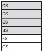
11 Intel 8086 Programming model
12 Intel 8086 Programming model The programming model contains 8, 16, and 32-bit registers. And some contains 64-bit registers when operated in the 64-bit mode The 8-bit registers are AH, AL, BH, BL, CH, CL, DH, and DL and are referred using two-letter designations (ADD AL,AH instruction adds the 8-bit contents of AH to AL, only AL changes due to instruction.) The 16-bit registers are AX, BX, CX, DX, SP, BP, DI, SI, IP, FLAGS, CS, DS, ES, SS, FS, and GS. Some of them consists of tow 8-bit registers (AX=AH + AL). The 16-bit registers are referenced with the two-letter designations such as AX ( ADD DX, CX instruction adds the 16-bit contents of CX to DX, Only DX changes due to this instruction). The extended 32-bit registers are EAX, EBX, ECX, EDX, ESP, EBP, EDI, ESI, EIP, and EFLAGS. These 32-bit extended registers, and 16-bit registers FS and GS( ADD ECX, EBX adds the 32-bit contents of EBX to ECX, Only ECX changes due to this instruction).
13 Intel 8086 Programming model General-purpose registers: include EAX, EBX, ECX, EDX, EBP, EDI, and ESI. Hold various data sizes (bytes, words, or double words) and are used for almost any purpose, as dictated by a program. RAX (accumulator), RBX (base index), Special Purpose registers include RIP, RSP, and RFLAGS; and the segment registers include CS, DS, ES, SS, FS, and GS. RIP (instruction register), RSP (Stack pointer),rflags (indicate the condition of the microprocessor and control its operation such as (C carry), (P parity ), (Z zero), (S Sign), (I interrupt), (O Overflow),...
14 how to interface: Chapter Objectives Explain how to interface both RAM and ROM to a microprocessor. Memory to an 8-, 16-, 32-, and 64-bit data bus by using various memory address sizes. Decode the memory address and use the outputs to select various memory components. Use programmable logic devices (PLDs) to decode memory addresses. Explain how error correction code (ECC) is used with memory. Explain the operation of a dynamic RAM controller. Interface dynamic RAM to the microprocessor
15 Introduction Every microprocessor-based system has a memory system. There are two main types of memory: Read-Only memory (ROM). contains system software and permanent system data. Random Access Memory (RAM) or read/write memory, contains temporary data and application software. This allows virtually any microprocessor to be interfaced to any memory system.
16 Common Types of Memory Devices There are four common types of memory: read-only memory (ROM) flash memory (EEPROM) static random access memory (SRAM) dynamic random access memory (DRAM).

17 Computer Memory Computers employ many different types of memory to hold data and programs. Semi-conductor Memories magnetic disks, USB sticks, DVDs etc.) Each type has its own characteristics and uses.
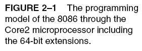
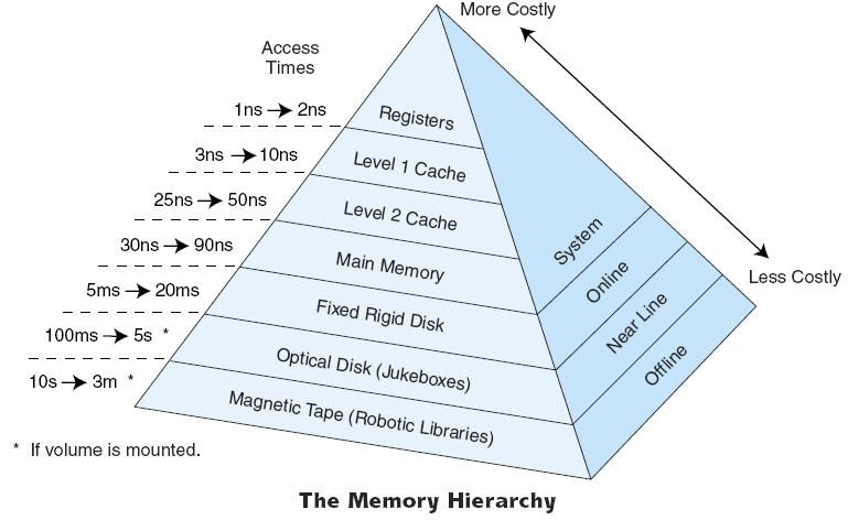
18 Memory Hierarchy For the same price: CPU processing speed (the number of instructions executed per second) has doubled every 18 months. Computer memory has quadrupling in size every 36 months. Memory speed, has increased at a rate of less than 10% per year. A gap between the speed of the processor and the speed of memory also increases.
19 Memory Hierarchy A computer have several types of memory, ranging from fast, expensive internal registers, to slow, inexpensive Hard Magnetic Disks. Registers: are matched in speed to the CPU consume a significant amount of power. only a small number of registers in a processor more expensive. Secondary storage: such as hard magnetic disks. the cost per stored bit is small in terms of money and electrical power. Access time is very long when compared with registers. Between the registers and secondary storage there are a number of other forms of memory that bridge the gap between the two.
20 Memory Hierarchy The memory hierarchy can be characterized by a number of parameters: Access Type: how physically the memory read/write is done (Random or Sequential). Capacity measured in bytes or KB or MB. Cycle time: the time elapsed from the start of a read operation to the start of a next read. Latency is defined as the time interval between the request for information and the access to the first bit of that information. Bandwidth: the number of bits that can be accessed in one second. Cost of a memory is usually specified as dollars/mb Total Cost = cost/mb * Memory Size.
21

22 The Memory Hierarchy Typical Cost = Cost/MB * Typical Amount
23
24
25 Memory Hierarchy Memory terminology: Hit: The requested data resides in a given level of memory. Miss: The requested data is not found in the given level of memory. Hit rate: The percentage of memory accesses found in a given level of memory. Miss rate: The percentage of memory accesses not found in a given level of memory. Miss Rate = 1 - Hit Rate. Hit time: The time required to access the requested information in a given level of memory.
26 Memory Hierarchy The processor makes a request for an item in memory as follows: The CPU tries to find the item in the first memory level of the memory hierarchy with hit ratio=h 1 or miss ratio=1-h 1. In case of miss, CPU tries to find the item in the second memory level with hit ratio, h 2 or miss ratio =1- h 2. The process is repeated until the item is found. In three levels memory hierarchy, the average memory access time can be expressed as follows: t 1, t 2, t 3 represent, the access times of the three levels
27 Main Memory The Figure shows an interface between the main memory and the CPU using two CPU registers: MAR (Memory Address Register): used to store the address of specific location. MDR (Memory Data Register): used to hold the data to be stored and/or retrieved in/from the memory location
28 Main Memory Internal Structure Main memory consists of: rows and columns of basic cells that store one bit of information. Cells in one row can be used to form a memory word. Address lines A n-1 A n-2.. A 1 A 0 are used as inputs to the address decoder in order to generate the word select lines W 2 n -1...W 1 W 0. A given word select line is common to all memory cells in the same row and is used to enable all cells in a row for read or write. Data (bit) lines are used to input or output the contents of cells. Each memory cell is connected to two data lines. A given data line is common to all cells in a given column.
29 2-1/2D Organization of a 64-Word by One-Bit RAM
30 Main Memory Internal Structure
31 All Memory devices have the following pins: Memory Pin connections Address input Pins Data input/output Pins Selection input Pins Control input Pins
32 Address Connections Used to select a memory location within the device. Labeled from A 0 (least significant address input), to A n-1 where n can be any value. No. of address pins = Log 2 (Memory Locations) No. of Memory Locations = 2 (Address Pins) A 1K memory device has 1024 memory locations and 10 address pins. It takes a 10-bit binary number to select any single location on a 1024-location device different combinations if a device has 11 address connections, it has 2 11 =2048 bit = 2KB internal memory locations
33 Address Input Pins The number 400H ( )B 1K-byte section of the memory system. represents a If a memory device is decoded to begin at memory address 10000H and it is a 1K device, its last location is at address (10000H + 400H)-1H = 103FFH one location less than 400H. 1000H is 4K. A memory device that contains a starting address of 14000H that is 4K bytes long ends at location 14FFFH one location less than 1000H. A third number is 64K, or 10000H. A memory that starts at location 30000H and ends at location 3FFFFH is a 64K-byte memory.
34 Data Connections All memory devices have a set of data outputs or input/outputs (bidirectional common I/O pins). data connections are points at which data are entered for storage (WRITE) or extracted for reading Data pins are labeled D0 through D7 for an 8-bit-wide memory device ( byte-wide memory ). most devices are 8 bits wide, some are 16 bits, 4 bits, or just 1 bit wide A memory device with 1K memory locations and 8 bits in each location is often listed as a 1K 8 by the manufacturer Memory devices are often classified according to total bit capacity.
35 Selection Connections Each memory device has an input that selects or enables the memory device ( sometimes more than one) This type of input is most often called a Chip Select (CS) Chip Enable (CE) or simply Select (S) input. RAM memory generally has at least one or tow inputs, and ROM has at least one If more than one CE connection is present, all must be activated to read or write data.
36 Control Connections ROM usually has one control input OE (Output Enable) allows data flow from output data pins. The OE enables and disables a set of three-state buffers located in the device and must be active to read data. RAM has either one or two control inputs: if one control input, it is often called R/W (Read / Write) If the RAM has two control inputs: WE write enable must be active to perform memory write. OE Output Enable must be active to perform a memory read when the two controls are present, they must never both be active at the same time If both inputs are inactive, data are neither written nor read. the connections are at their high-impedance state.
37 Main Memory Cell Each main memory cell consists of six CMOS transistors,the six transistor static CMOS memory cell consists of two inverters back to back.
38 Main Memory Cell
39 Memory Design Design a 1KX4 memory chip. It can be designed as where n=10, 1K rows of cells, each consisting of four cells. The chip will then have to have 10 pins for the address and four pins for the data. This not the Best utilization of chip area.
40 Design a 1KX4 memory chip. It can be designed as 64 rows, each consisting of 64 cells. In this case, 6 address lines forming the row address. The remaining 4 address lines (column address) will be used to select the appropriate 4 bits among the available 64 bits constituting a row. Memory Design Factors
41 Memory Design Design a 4k bits memory chip. Different organization of the same memory capacity can lead to a different number of chip pins requirement. It is clear from the table that increasing the number of bits per addressable location results in an increase in the number of pins needed in the integrated circuit.
42 Random Access Memory Random means that any memory location can be accessed in the same amount of time, regardless of its position in the memory. D flip-flop, with additional controls to allow the cell to be selected, read, and written. There is a (bidirectional) data line for data input and output. Static RAM cell (a) and dynamic RAM cell (b).
43 A Four-Word Memory with Four Bits per Word in a 2D Organization.
44 A Simplified Representation of the Four-Word by Four-Bit RAM Creating a Four-Word by Eight-Bit RAM using Two Four-Word by Four-Bit RAMs.
45 Two Four-Word by Four-Bit RAMs Make up an Eight-Word by Four-Bit RAM
46 ROM Memory The read-only memory (ROM): permanently stores programs and data that are resident to the system and must not change when power supply is disconnected. The ROM is permanently programmed non-volatile memory, because its contents do not change even if power is disconnected. Today, the ROM is available in many forms. A device we call a ROM is purchased in mass quantities from a manufacturer and programmed during its fabrication at the factory.
47 ROM Memory (EPROM and PROM) The EPROM (erasable programmable read-only memory), a type of ROM, is more commonly used when software must be changed often or when too few are in demand to make the ROM economical. An EPROM is programmed in the field on a device called an EPROM programmer. The EPROM is also erasable if exposed to high-intensity ultraviolet light for about 20 minutes or so, depending on the type of EPROM. The PROM (programmable read-only memory) is also programmed in the field by burning open tiny NI-chrome or silicon oxide fuses; but once it is programmed, it cannot be erased.
48 ROM Memory (Flash Memory) The flash memory is also often called an EEPROM (electrically erasable programmable ROM),or a NOVRAM (non-volatile RAM). Are electrically erasable in the system, but they require more time to erase than a normal RAM. The flash memory device is used to store setup information for systems such as the video card in the computer. It has all but replaced the EPROM in most computer systems for the BIOS memory. Some systems contain a password stored in the flash memory device. Flash memory has its biggest impact in memory cards for digital cameras and memory in MP3 audio players.
49 ROM Memory (Flash Memory)
50 A ROM Stores Four Four-Bit Words
51 ROM Memory (Flash Memory) Data appear on the output connections only after a logic 0 is placed on both CE and OE pin connections. If CE and OE are not both logic 0s, the data output connections remain at their high-impedance or off states. Note that the V PP pin must be placed at a logic 1 level for data to be read from the EPROM. In some cases, the V PP pin is in the same position as the WE pin on the SRAM. This will allow a single socket to hold either an EPROM or an SRAM.
52 ROM Memory (Flash Memory)
53 ROM Memory (Flash Memory)

54 Flash Memory (a) External view of flash memory module and (b) flash module internals. (Source: adapted from HowStuffWorks.com.)
55 Memory Access Time Memory access time T ACC the time that it takes the memory to read information. T ACC is measured from the appearance of the address at the address inputs until the appearance of the data at the output connections. This is based on the assumption that the CE input goes low at the same time that the address inputs become stable. Also, OE must be a logic 0 for the output connections to become active. The basic speed of EPROM is 450 ns. And 086/8088 operated with a 5 MHz clock allowed memory 460 ns to access data. Wait states are required to operate properly with the 8086/8088 microprocessors.
56 Static RAM Devices is a RAM chips that are based upon flip-flops, because the contents of each location persist as long as power is applied to the chips. Static RAM memory devices retain data for as long as DC power is applied. Because no special action (except power) is required to retain stored data, these devices are called static memory. They are also called volatile memory because they will not retain data without power. The SRAM, which stores temporary data, is used when the size of the read/write memory is relatively small.
57 Static RAM Devices
58 Static RAM Devices
59 Static RAM Devices
60 Static RAM Devices
61 Static RAM Devices
62 Dynamic RAM Devices DRAM The same as SRAM, except that it retains data for only 2 or 4 ms on an integrated capacitor. After 2 or 4 ms, the contents of the DRAM must be completely rewritten (refreshed) because the capacitors, which store a logic 1 or logic 0, lose their charges. Refresh is reading the content of memory location and write it again which is impossible task. This occurs during write, read or during special refresh cycle. the manufacturer has internally constructed the DRAM differently from the SRAM. So that, the entire content of the memory are refreshed with 256 reads in a 2-4-ms. DRAM requires so many address pins that the manufacturers have decided to multiplex the address
63 Dynamic RAM Devices DRAM Is a RAM chips, employ a capacitor, which stores a minute amount of electric charge, in which the charge level represents a 1 or a 0. Capacitors are much smaller than flip-flops, so a capacitor based DRAM can hold much more information in the same area than an SRAM. Since the charges on the capacitors dissipate with time, the charge in the capacitor storage cells in DRAMs must be restored, or refreshed frequently.
64 Dynamic RAM Devices DRAM
65 Dynamic RAM Devices DRAM A DRAM 64K 4 DRAM, which stores 256K bits of data. Can use only eight address inputs instead of 16 the number required to address 64K memory locations. The Multiplexing operation requires two special pins: the column address strobe (CAS ) and row address strobe ( RAS). First, A0 A7 are placed on the address pins and strobed into an internal row latch by RAS as the row address. Next, the address bits A8--A15 are placed on the same eight address inputs and strobed into an internal column latch by CAS as the column address. The 16-bit address held in these internal latches addresses the contents of one of the 4-bit memory locations.
66 Dynamic RAM Devices DRAM
67 Dynamic RAM Devices DRAM
68 Dynamic RAM Devices DRAM DRAM memory is often placed on small circuit boards called SIMMs (Single In-Line Memory Modules). The 30-pin SIMM is organized most often as 1M 8 or 1M 9, and 4M 8 or 4M 9. The ninth bit is the parity bit. Also shown is a newer 72 pin SIMM. The 72-pin SIMMs are often organized as 1M 32 or 1M 36 (with parity). Other sizes are 2M 32, 4M 32, 8M 32, and 16M 32. These are also available with parity.
69 Dynamic RAM Devices DRAM Pentium 4 microprocessors have a 64-bit wide data bus, SIMMs must be used in pairs to obtain a 64-bit-wide data connection. Today, the 64-bit-wide DIMMs (Dual In-line Memory Modules) have become the standard in most systems. The memory on these modules is organized as 64 bits wide. The common sizes available are 16M bytes (2M 64), 32M bytes (4M 64), 64M bytes (8M 64), 128M bytes (16M 64), 256M bytes (32M 64), 512M bytes (64M 64), and 1G bytes (128M 64).
70 Dynamic RAM Devices DRAM
71 Dynamic RAM Devices DRAM
72 Sheet 1 1. What types of connections are common to all memory devices? 2. List the number of words found in each memory device for the following numbers of address connections: (a) 8 (b) 11 (c) 12 (d) 13 (e) List the number of data items stored in each of the following memory devices and the number of bits in each datum: 4. (a) 2K 4 (b) 1K l (c) 4K 8 (d) 16K 1 (e) 64K 4 5. What is the purpose of the CS or CE pin on a memory component? 6. What is the purpose of theoe pin on a memory device? 7. What is the purpose of the WE pin on a SRAM? 8. How many bytes of storage do the following EPROM memory devices contain? (a) 2708 (b) 2716 (c) 2732 (d) 2764 (e) 27512
73 Sheet 1 9. Why won t a 450 ns EPROM work directly with a 5 MHz 8088? 10. What can be stated about the amount of time needed to erase and write a location in a flash memory device? 11. SRAM is an acronym for what type of device? 12. The 4016 memory has a G pin, S and W pin, and a pin. What are these pins used for in this RAM? 13. How much memory access time is required by the slowest 4016? 14. DRAM is an acronym for what type of device? 15. The 256M DIMM has 28 address inputs, yet it is a 256M DRAM. Explain how a 28-bit memory address is forced into 14 address inputs. 16. What are the purposes of the CAS and RAS inputs of a DRAM? 17. How much time is required to refresh the typical DRAM?
Introduction read-only memory random access memory
 Memory Interface Introduction Simple or complex, every microprocessorbased system has a memory system. Almost all systems contain two main types of memory: read-only memory (ROM) and random access memory
Hardware and Software Architecture. Chapter 2
 Hardware and Software Architecture Chapter 2 1 Basic Components The x86 processor communicates with main memory and I/O devices via buses Data bus for transferring data Address bus for the address of a
CS 16: Assembly Language Programming for the IBM PC and Compatibles
 CS 16: Assembly Language Programming for the IBM PC and Compatibles Discuss the general concepts Look at IA-32 processor architecture and memory management Dive into 64-bit processors Explore the components
Lecture (02) The Microprocessor and Its Architecture By: Dr. Ahmed ElShafee
 The Microprocessor and Its Architecture By: Dr. Ahmed ElShafee") Lecture (02) The Microprocessor and Its Architecture By: Dr. Ahmed ElShafee ١ INTERNAL MICROPROCESSOR ARCHITECTURE Before a program is written or instruction investigated, internal configuration of the
Lecture (02) The Microprocessor and Its Architecture By: Dr. Ahmed ElShafee ١ INTERNAL MICROPROCESSOR ARCHITECTURE Before a program is written or instruction investigated, internal configuration of the
Memory Overview. Overview - Memory Types 2/17/16. Curtis Nelson Walla Walla University
 Memory Overview Curtis Nelson Walla Walla University Overview - Memory Types n n n Magnetic tape (used primarily for long term archive) Magnetic disk n Hard disk (File, Directory, Folder) n Floppy disks
EEM336 Microprocessors I. The Microprocessor and Its Architecture
 EEM336 Microprocessors I The Microprocessor and Its Architecture Introduction This chapter presents the microprocessor as a programmable device by first looking at its internal programming model and then
UMBC. Select. Read. Write. Output/Input-output connection. 1 (Feb. 25, 2002) Four commonly used memories: Address connection ... Dynamic RAM (DRAM)
 Four commonly used memories: Address connection ... Dynamic RAM (DRAM)") Memory Types Two basic types: ROM: Read-only memory RAM: Read-Write memory Four commonly used memories: ROM Flash (EEPROM) Static RAM (SRAM) Dynamic RAM (DRAM) Generic pin configuration: Address connection
Memory Types Two basic types: ROM: Read-only memory RAM: Read-Write memory Four commonly used memories: ROM Flash (EEPROM) Static RAM (SRAM) Dynamic RAM (DRAM) Generic pin configuration: Address connection
6/17/2011. Introduction. Chapter Objectives Upon completion of this chapter, you will be able to:
 Chapter 2: The Microprocessor and its Architecture Chapter 2: The Microprocessor and its Architecture Chapter 2: The Microprocessor and its Architecture Introduction This chapter presents the microprocessor
Concept of Memory. The memory of computer is broadly categories into two categories:
 Concept of Memory We have already mentioned that digital computer works on stored programmed concept introduced by Von Neumann. We use memory to store the information, which includes both program and data.
EC-333 Microprocessor and Interfacing Techniques
 EC-333 Microprocessor and Interfacing Techniques Lecture 3 The Microprocessor and its Architecture Dr Hashim Ali Fall - 2018 Department of Computer Science and Engineering HITEC University Taxila Slides
Chapter 2: The Microprocessor and its Architecture
 Chapter 2: The Microprocessor and its Architecture Chapter 2: The Microprocessor and its Architecture Chapter 2: The Microprocessor and its Architecture Introduction This chapter presents the microprocessor
EXPERIMENT WRITE UP. LEARNING OBJECTIVES: 1. Get hands on experience with Assembly Language Programming 2. Write and debug programs in TASM/MASM
 EXPERIMENT WRITE UP AIM: Assembly language program for 16 bit BCD addition LEARNING OBJECTIVES: 1. Get hands on experience with Assembly Language Programming 2. Write and debug programs in TASM/MASM TOOLS/SOFTWARE
The Microprocessor and its Architecture
 The Microprocessor and its Architecture Contents Internal architecture of the Microprocessor: The programmer s model, i.e. The registers model The processor model (organization) Real mode memory addressing
Moodle WILLINGDON COLLEGE SANGLI (B. SC.-II) Digital Electronics
 Digital Electronics") Moodle 4 WILLINGDON COLLEGE SANGLI (B. SC.-II) Digital Electronics Advanced Microprocessors and Introduction to Microcontroller Moodle developed By Dr. S. R. Kumbhar Department of Electronics Willingdon
Moodle 4 WILLINGDON COLLEGE SANGLI (B. SC.-II) Digital Electronics Advanced Microprocessors and Introduction to Microcontroller Moodle developed By Dr. S. R. Kumbhar Department of Electronics Willingdon
Address connections Data connections Selection connections
 Interface (cont..) We have four common types of memory: Read only memory ( ROM ) Flash memory ( EEPROM ) Static Random access memory ( SARAM ) Dynamic Random access memory ( DRAM ). Pin connections common
Allmost all systems contain two main types of memory :
 Memory Interface Allmost all systems contain two main types of memory : read-only memory (ROM) system software and permanent system data random access memory (RAM) or read/write memory application software
Assembly Language for x86 Processors 7 th Edition. Chapter 2: x86 Processor Architecture
 Assembly Language for x86 Processors 7 th Edition Kip Irvine Chapter 2: x86 Processor Architecture Slides prepared by the author Revision date: 1/15/2014 (c) Pearson Education, 2015. All rights reserved.
7/6/2011. Introduction. Chapter Objectives Upon completion of this chapter, you will be able to:
 Introduction Simple or complex, every microprocessorbased system has a memory system. Almost all systems contain two main types of memory: read-only memory (ROM) and random access memory (RAM) or read/write
Addressing Modes on the x86
 Addressing Modes on the x86 register addressing mode mov ax, ax, mov ax, bx mov ax, cx mov ax, dx constant addressing mode mov ax, 25 mov bx, 195 mov cx, 2056 mov dx, 1000 accessing data in memory There
COMP3221: Microprocessors and. and Embedded Systems. Overview. Lecture 23: Memory Systems (I)
") COMP3221: Microprocessors and Embedded Systems Lecture 23: Memory Systems (I) Overview Memory System Hierarchy RAM, ROM, EPROM, EEPROM and FLASH http://www.cse.unsw.edu.au/~cs3221 Lecturer: Hui Wu Session
COMP3221: Microprocessors and Embedded Systems Lecture 23: Memory Systems (I) Overview Memory System Hierarchy RAM, ROM, EPROM, EEPROM and FLASH http://www.cse.unsw.edu.au/~cs3221 Lecturer: Hui Wu Session
Lecture 15 Intel Manual, Vol. 1, Chapter 3. Fri, Mar 6, Hampden-Sydney College. The x86 Architecture. Robb T. Koether. Overview of the x86
 Lecture 15 Intel Manual, Vol. 1, Chapter 3 Hampden-Sydney College Fri, Mar 6, 2009 Outline 1 2 Overview See the reference IA-32 Intel Software Developer s Manual Volume 1: Basic, Chapter 3. Instructions
IA-32 Architecture COE 205. Computer Organization and Assembly Language. Computer Engineering Department
 IA-32 Architecture COE 205 Computer Organization and Assembly Language Computer Engineering Department King Fahd University of Petroleum and Minerals Presentation Outline Basic Computer Organization Intel
We can study computer architectures by starting with the basic building blocks. Adders, decoders, multiplexors, flip-flops, registers,...
 COMPUTER ARCHITECTURE II: MICROPROCESSOR PROGRAMMING We can study computer architectures by starting with the basic building blocks Transistors and logic gates To build more complex circuits Adders, decoders,
machine cycle, the CPU: (a) Fetches an instruction, (b) Decodes the instruction, (c) Executes the instruction, and (d) Stores the result.
 Fetches an instruction, (b) Decodes the instruction, (c) Executes the instruction, and (d) Stores the result.") Central Processing Unit (CPU) A processor is also called the CPU, and it works hand in hand with other circuits known as main memory to carry out processing. The CPU is the "brain" of the computer; it
Central Processing Unit (CPU) A processor is also called the CPU, and it works hand in hand with other circuits known as main memory to carry out processing. The CPU is the "brain" of the computer; it
211: Computer Architecture Summer 2016
 211: Computer Architecture Summer 2016 Liu Liu Topic: Assembly Programming Storage - Assembly Programming: Recap - project2 - Structure/ Array Representation - Structure Alignment Rutgers University Liu
CREATED BY M BILAL & Arslan Ahmad Shaad Visit:
 CREATED BY M BILAL & Arslan Ahmad Shaad Visit: www.techo786.wordpress.com Q1: Define microprocessor? Short Questions Chapter No 01 Fundamental Concepts Microprocessor is a program-controlled and semiconductor
Computer Organization and Assembly Language (CS-506)
") Computer Organization and Assembly Language (CS-506) Muhammad Zeeshan Haider Ali Lecturer ISP. Multan ali.zeeshan04@gmail.com https://zeeshanaliatisp.wordpress.com/ Lecture 2 Memory Organization and Structure
Computer Organization and Assembly Language (CS-506) Muhammad Zeeshan Haider Ali Lecturer ISP. Multan ali.zeeshan04@gmail.com https://zeeshanaliatisp.wordpress.com/ Lecture 2 Memory Organization and Structure
For your convenience Apress has placed some of the front matter material after the index. Please use the Bookmarks and Contents at a Glance links to
 For your convenience Apress has placed some of the front matter material after the index. Please use the Bookmarks and Contents at a Glance links to access them. Contents at a Glance About the Author...xi
k -bit address bus n-bit data bus Control lines ( R W, MFC, etc.)
") THE MEMORY SYSTEM SOME BASIC CONCEPTS Maximum size of the Main Memory byte-addressable CPU-Main Memory Connection, Processor MAR MDR k -bit address bus n-bit data bus Memory Up to 2 k addressable locations
THE MEMORY SYSTEM SOME BASIC CONCEPTS Maximum size of the Main Memory byte-addressable CPU-Main Memory Connection, Processor MAR MDR k -bit address bus n-bit data bus Memory Up to 2 k addressable locations
Microcontroller Systems. ELET 3232 Topic 11: General Memory Interfacing
 Microcontroller Systems ELET 3232 Topic 11: General Memory Interfacing 1 Objectives To become familiar with the concepts of memory expansion and the data and address bus To design embedded systems circuits
chapter 8 The Memory System Chapter Objectives
 chapter 8 The Memory System Chapter Objectives In this chapter you will learn about: Basic memory circuits Organization of the main memory Memory technology Direct memory access as an I/O mechanism Cache
3 Computer Architecture and Assembly Language
 3 Computer Architecture and Assembly Language 3.1 Overview of the Organization of a Computer System All general-purpose computers require the following hardware components: Main memory: enables a computer
The x86 Microprocessors. Introduction. The 80x86 Microprocessors. 1.1 Assembly Language
 The x86 Microprocessors Introduction 1.1 Assembly Language Numbering and Coding Systems Human beings use the decimal system (base 10) Decimal digits: 0, 1, 2, 3, 4, 5, 6, 7, 8, 9 Computer systems use the
THE MICROCOMPUTER SYSTEM CHAPTER - 2
 THE MICROCOMPUTER SYSTEM CHAPTER - 2 20 2.1 GENERAL ASPECTS The first computer was developed using vacuum tubes. The computers thus developed were clumsy and dissipating more power. After the invention
The x86 Architecture
 The x86 Architecture Lecture 24 Intel Manual, Vol. 1, Chapter 3 Robb T. Koether Hampden-Sydney College Fri, Mar 20, 2015 Robb T. Koether (Hampden-Sydney College) The x86 Architecture Fri, Mar 20, 2015
Basic Organization Memory Cell Operation. CSCI 4717 Computer Architecture. ROM Uses. Random Access Memory. Semiconductor Memory Types
 CSCI 4717/5717 Computer Architecture Topic: Internal Memory Details Reading: Stallings, Sections 5.1 & 5.3 Basic Organization Memory Cell Operation Represent two stable/semi-stable states representing
UNIT V (PROGRAMMABLE LOGIC DEVICES)
") UNIT V (PROGRAMMABLE LOGIC DEVICES) Introduction There are two types of memories that are used in digital systems: Random-access memory(ram): perform both the write and read operations. Read-only memory(rom):
UNIT V (PROGRAMMABLE LOGIC DEVICES) Introduction There are two types of memories that are used in digital systems: Random-access memory(ram): perform both the write and read operations. Read-only memory(rom):
ECE 341. Lecture # 16
 ECE 341 Lecture # 16 Instructor: Zeshan Chishti zeshan@ece.pdx.edu November 24, 2014 Portland State University Lecture Topics The Memory System Basic Concepts Semiconductor RAM Memories Organization of
8051 INTERFACING TO EXTERNAL MEMORY
 8051 INTERFACING TO EXTERNAL MEMORY Memory Capacity The number of bits that a semiconductor memory chip can store Called chip capacity It can be in units of Kbits (kilobits), Mbits (megabits), and so on
UNIT:4 MEMORY ORGANIZATION
 1 UNIT:4 MEMORY ORGANIZATION TOPICS TO BE COVERED. 4.1 Memory Hierarchy 4.2 Memory Classification 4.3 RAM,ROM,PROM,EPROM 4.4 Main Memory 4.5Auxiliary Memory 4.6 Associative Memory 4.7 Cache Memory 4.8
COMP2121: Microprocessors and Interfacing. Introduction to Microprocessors
 COMP2121: Microprocessors and Interfacing Introduction to Microprocessors http://www.cse.unsw.edu.au/~cs2121 Lecturer: Hui Wu Session 2, 2017 1 1 Contents Processor architectures Bus Memory hierarchy 2
Contents. Main Memory Memory access time Memory cycle time. Types of Memory Unit RAM ROM
 Memory Organization Contents Main Memory Memory access time Memory cycle time Types of Memory Unit RAM ROM Memory System Virtual Memory Cache Memory - Associative mapping Direct mapping Set-associative
Overview. Memory Classification Read-Only Memory (ROM) Random Access Memory (RAM) Functional Behavior of RAM. Implementing Static RAM
 Random Access Memory (RAM) Functional Behavior of RAM. Implementing Static RAM") Memories Overview Memory Classification Read-Only Memory (ROM) Types of ROM PROM, EPROM, E 2 PROM Flash ROMs (Compact Flash, Secure Digital, Memory Stick) Random Access Memory (RAM) Types of RAM Static
Memories Overview Memory Classification Read-Only Memory (ROM) Types of ROM PROM, EPROM, E 2 PROM Flash ROMs (Compact Flash, Secure Digital, Memory Stick) Random Access Memory (RAM) Types of RAM Static
DIGITAL SYSTEM FUNDAMENTALS (ECE421) DIGITAL ELECTRONICS FUNDAMENTAL (ECE422)
 DIGITAL ELECTRONICS FUNDAMENTAL (ECE422)") COURSE / CODE DIGITAL SYSTEM FUNDAMENTALS (ECE421) DIGITAL ELECTRONICS FUNDAMENTAL (ECE422) Memory In computing, memory refers to the computer hardware devices used to store information for immediate use
COURSE / CODE DIGITAL SYSTEM FUNDAMENTALS (ECE421) DIGITAL ELECTRONICS FUNDAMENTAL (ECE422) Memory In computing, memory refers to the computer hardware devices used to store information for immediate use
MICROPROCESSOR MCQs. 1) What does the microprocessor comprise of? a. Register section b. One or more ALU c. Control unit d.
 What does the microprocessor comprise of? a. Register section b. One or more ALU c. Control unit d.") 1) What does the microprocessor comprise of? a. Register section b. One or more ALU c. Control unit 2) What is stored by a register? a. data b. operands c. memory MICROPROCESSOR MCQs 3) Accumulator based
1) What does the microprocessor comprise of? a. Register section b. One or more ALU c. Control unit 2) What is stored by a register? a. data b. operands c. memory MICROPROCESSOR MCQs 3) Accumulator based
Read and Write Cycles
 Read and Write Cycles The read cycle is shown. Figure 41.1a. The RAS and CAS signals are activated one after the other to latch the multiplexed row and column addresses respectively applied at the multiplexed
William Stallings Computer Organization and Architecture 6th Edition. Chapter 5 Internal Memory
 William Stallings Computer Organization and Architecture 6th Edition Chapter 5 Internal Memory Semiconductor Memory Types Semiconductor Memory RAM Misnamed as all semiconductor memory is random access
The Memory Component
 The Computer Memory Chapter 6 forms the first of a two chapter sequence on computer memory. Topics for this chapter include. 1. A functional description of primary computer memory, sometimes called by
Introduction to IA-32. Jo, Heeseung
 Introduction to IA-32 Jo, Heeseung IA-32 Processors Evolutionary design Starting in 1978 with 8086 Added more features as time goes on Still support old features, although obsolete Totally dominate computer
Computer Processors. Part 2. Components of a Processor. Execution Unit The ALU. Execution Unit. The Brains of the Box. Processors. Execution Unit (EU)
") Part 2 Computer Processors Processors The Brains of the Box Computer Processors Components of a Processor The Central Processing Unit (CPU) is the most complex part of a computer In fact, it is the computer
Part 2 Computer Processors Processors The Brains of the Box Computer Processors Components of a Processor The Central Processing Unit (CPU) is the most complex part of a computer In fact, it is the computer
INTRODUCTION TO IA-32. Jo, Heeseung
 INTRODUCTION TO IA-32 Jo, Heeseung IA-32 PROCESSORS Evolutionary design Starting in 1978 with 8086 Added more features as time goes on Still support old features, although obsolete Totally dominate computer
CENG4480 Lecture 09: Memory 1
 CENG4480 Lecture 09: Memory 1 Bei Yu byu@cse.cuhk.edu.hk (Latest update: November 8, 2017) Fall 2017 1 / 37 Overview Introduction Memory Principle Random Access Memory (RAM) Non-Volatile Memory Conclusion
CS429: Computer Organization and Architecture
 CS429: Computer Organization and Architecture Dr. Bill Young Department of Computer Sciences University of Texas at Austin Last updated: November 28, 2017 at 14:31 CS429 Slideset 18: 1 Random-Access Memory
CS 320 February 2, 2018 Ch 5 Memory
 CS 320 February 2, 2018 Ch 5 Memory Main memory often referred to as core by the older generation because core memory was a mainstay of computers until the advent of cheap semi-conductor memory in the
CS429: Computer Organization and Architecture
 CS429: Computer Organization and Architecture Dr. Bill Young Department of Computer Sciences University of Texas at Austin Last updated: April 9, 2018 at 12:16 CS429 Slideset 17: 1 Random-Access Memory
Assembly Language Each statement in an assembly language program consists of four parts or fields.
 Chapter 3: Addressing Modes Assembly Language Each statement in an assembly language program consists of four parts or fields. The leftmost field is called the label. - used to identify the name of a memory
UNIT-V MEMORY ORGANIZATION
 UNIT-V MEMORY ORGANIZATION 1 The main memory of a computer is semiconductor memory.the main memory unit is basically consists of two kinds of memory: RAM (RWM):Random access memory; which is volatile in
Memory and Programmable Logic
 Memory and Programmable Logic Memory units allow us to store and/or retrieve information Essentially look-up tables Good for storing data, not for function implementation Programmable logic device (PLD),
CENG3420 Lecture 08: Memory Organization
 CENG3420 Lecture 08: Memory Organization Bei Yu byu@cse.cuhk.edu.hk (Latest update: February 22, 2018) Spring 2018 1 / 48 Overview Introduction Random Access Memory (RAM) Interleaving Secondary Memory
Computer Organization. 8th Edition. Chapter 5 Internal Memory
 William Stallings Computer Organization and Architecture 8th Edition Chapter 5 Internal Memory Semiconductor Memory Types Memory Type Category Erasure Write Mechanism Volatility Random-access memory (RAM)
Components of a personal computer
 Components of a personal computer Computer systems ranging from a controller in a microwave oven to a large supercomputer contain components providing five functions. A typical personal computer has hard,
ECE 485/585 Microprocessor System Design
 Microprocessor System Design Lecture 4: Memory Hierarchy Memory Taxonomy SRAM Basics Memory Organization DRAM Basics Zeshan Chishti Electrical and Computer Engineering Dept Maseeh College of Engineering
Instruction Set Architectures
 Instruction Set Architectures Computer Systems: Section 4.1 Suppose you built a computer What Building Blocks would you use? Arithmetic Logic Unit (ALU) OP1 OP2 OPERATION ALU RES ALU + Registers R0: 0x0000
Assembler Programming. Lecture 2
 Assembler Programming Lecture 2 Lecture 2 8086 family architecture. From 8086 to Pentium4. Registers, flags, memory organization. Logical, physical, effective address. Addressing modes. Processor Processor
Chapter 5 Internal Memory
 Chapter 5 Internal Memory Memory Type Category Erasure Write Mechanism Volatility Random-access memory (RAM) Read-write memory Electrically, byte-level Electrically Volatile Read-only memory (ROM) Read-only
Microprocessor (COM 9323)
") Microprocessor (COM 9323) Lecture 3: The Microprocessor and Its Architecture Ahmed Elnakib, PhD Assistant Professor, Mansoura University, Egypt Feb 24 th, 2016 1 Text Book/References* Textbook: The Intel
Microprocessor (COM 9323) Lecture 3: The Microprocessor and Its Architecture Ahmed Elnakib, PhD Assistant Professor, Mansoura University, Egypt Feb 24 th, 2016 1 Text Book/References* Textbook: The Intel
Program controlled semiconductor device (IC) which fetches (from memory), decodes and executes instructions.
 which fetches (from memory), decodes and executes instructions.") 8086 Microprocessor Microprocessor Program controlled semiconductor device (IC) which fetches (from memory), decodes and executes instructions. It is used as CPU (Central Processing Unit) in computers.
8086 Microprocessor Microprocessor Program controlled semiconductor device (IC) which fetches (from memory), decodes and executes instructions. It is used as CPU (Central Processing Unit) in computers.
Large and Fast: Exploiting Memory Hierarchy
 CSE 431: Introduction to Operating Systems Large and Fast: Exploiting Memory Hierarchy Gojko Babić 10/5/018 Memory Hierarchy A computer system contains a hierarchy of storage devices with different costs,
MICROPROCESSOR TECHNOLOGY
 MICROPROCESSOR TECHNOLOGY Assis. Prof. Hossam El-Din Moustafa Lecture 5 Ch.2 A Top-Level View of Computer Function (Cont.) 24-Feb-15 1 CPU (CISC & RISC) Intel CISC, Motorola RISC CISC (Complex Instruction
Menu. word size # of words byte = 8 bits
 Menu LSI Components >Random Access Memory (RAM) Static RAM (SRAM) Dynamic RAM (DRAM) Read-Only Memory (ROM) Look into my... See figures from Lam text on web: RAM_ROM_ch6.pdf 1 It can be thought of as 1
MODE (mod) FIELD CODES. mod MEMORY MODE: 8-BIT DISPLACEMENT MEMORY MODE: 16- OR 32- BIT DISPLACEMENT REGISTER MODE
 FIELD CODES. mod MEMORY MODE: 8-BIT DISPLACEMENT MEMORY MODE: 16- OR 32- BIT DISPLACEMENT REGISTER MODE") EXERCISE 9. Determine the mod bits from Figure 7-24 and write them in Table 7-7. MODE (mod) FIELD CODES mod 00 01 10 DESCRIPTION MEMORY MODE: NO DISPLACEMENT FOLLOWS MEMORY MODE: 8-BIT DISPLACEMENT MEMORY
EXERCISE 9. Determine the mod bits from Figure 7-24 and write them in Table 7-7. MODE (mod) FIELD CODES mod 00 01 10 DESCRIPTION MEMORY MODE: NO DISPLACEMENT FOLLOWS MEMORY MODE: 8-BIT DISPLACEMENT MEMORY
Module 5a: Introduction To Memory System (MAIN MEMORY)
") Module 5a: Introduction To Memory System (MAIN MEMORY) R E F E R E N C E S : S T A L L I N G S, C O M P U T E R O R G A N I Z A T I O N A N D A R C H I T E C T U R E M O R R I S M A N O, C O M P U T E
Module 5a: Introduction To Memory System (MAIN MEMORY) R E F E R E N C E S : S T A L L I N G S, C O M P U T E R O R G A N I Z A T I O N A N D A R C H I T E C T U R E M O R R I S M A N O, C O M P U T E
Assembly Language for Intel-Based Computers, 4 th Edition. Kip R. Irvine. Chapter 2: IA-32 Processor Architecture
 Assembly Language for Intel-Based Computers, 4 th Edition Kip R. Irvine Chapter 2: IA-32 Processor Architecture Chapter Overview General Concepts IA-32 Processor Architecture IA-32 Memory Management Components
Summer 2003 Lecture 18 07/09/03
 Summer 2003 Lecture 18 07/09/03 NEW HOMEWORK Instruction Execution Times: The 8088 CPU is a synchronous machine that operates at a particular clock frequency. In the case of the original IBM PC, that clock
Memory classification:- Topics covered:- types,organization and working
 Memory classification:- Topics covered:- types,organization and working 1 Contents What is Memory? Cache Memory PC Memory Organisation Types 2 Memory what is it? Usually we consider this to be RAM, ROM
Design with Microprocessors
 Design with Microprocessors Year III Computer Sci. English 1-st Semester Lecture 12: Memory interfacing Typical Memory Hierarchy [1] On-Chip Components Control edram Datapath RegFile ITLB DTLB Instr Data
Memory memories memory
 Memory Organization Memory Hierarchy Memory is used for storing programs and data that are required to perform a specific task. For CPU to operate at its maximum speed, it required an uninterrupted and
Intel 8086 MICROPROCESSOR ARCHITECTURE
 Intel 8086 MICROPROCESSOR ARCHITECTURE 1 Features It is a 16-bit μp. 8086 has a 20 bit address bus can access up to 2 20 memory locations (1 MB). It can support up to 64K I/O ports. It provides 14, 16
William Stallings Computer Organization and Architecture 8th Edition. Chapter 5 Internal Memory
 William Stallings Computer Organization and Architecture 8th Edition Chapter 5 Internal Memory Semiconductor Memory The basic element of a semiconductor memory is the memory cell. Although a variety of
Organization. 5.1 Semiconductor Main Memory. William Stallings Computer Organization and Architecture 6th Edition
 William Stallings Computer Organization and Architecture 6th Edition Chapter 5 Internal Memory 5.1 Semiconductor Main Memory 5.2 Error Correction 5.3 Advanced DRAM Organization 5.1 Semiconductor Main Memory
6/20/2011. Introduction. Chapter Objectives Upon completion of this chapter, you will be able to:
 Introduction Efficient software development for the microprocessor requires a complete familiarity with the addressing modes employed by each instruction. This chapter explains the operation of the stack
Memory Study Material
 Computer memory refers to the devices that are used to store data or programs on a temporary or permanent basis for use in a computer. Any data or instruction entered into the memory of a computer is considered
COA. Prepared By: Dhaval R. Patel Page 1. Q.1 Define MBR.
 Q.1 Define MBR. MBR( Memory buffer register) A Memory Buffer Register (MBR) is the register in a computers processor that stores the data being transferred to and from the devices It allowing the processor
CMSC 313 COMPUTER ORGANIZATION & ASSEMBLY LANGUAGE PROGRAMMING LECTURE 03, SPRING 2013
 CMSC 313 COMPUTER ORGANIZATION & ASSEMBLY LANGUAGE PROGRAMMING LECTURE 03, SPRING 2013 TOPICS TODAY Moore s Law Evolution of Intel CPUs IA-32 Basic Execution Environment IA-32 General Purpose Registers
Internal Memory. Computer Architecture. Outline. Memory Hierarchy. Semiconductor Memory Types. Copyright 2000 N. AYDIN. All rights reserved.
 Computer Architecture Prof. Dr. Nizamettin AYDIN naydin@yildiz.edu.tr nizamettinaydin@gmail.com Internal Memory http://www.yildiz.edu.tr/~naydin 1 2 Outline Semiconductor main memory Random Access Memory
Assembly Language for Intel-Based Computers, 4 th Edition. Chapter 2: IA-32 Processor Architecture. Chapter Overview.
 Assembly Language for Intel-Based Computers, 4 th Edition Kip R. Irvine Chapter 2: IA-32 Processor Architecture Slides prepared by Kip R. Irvine Revision date: 09/25/2002 Chapter corrections (Web) Printing
MICROPROCESSOR PROGRAMMING AND SYSTEM DESIGN
 MICROPROCESSOR PROGRAMMING AND SYSTEM DESIGN ROAD MAP SDK-86 Intel 8086 Features 8086 Block Diagram 8086 Architecture Bus Interface Unit Execution Unit 8086 Architecture 8086 Programmer s Model Flag Register
Memory & Simple I/O Interfacing
 Chapter 10 Memory & Simple I/O Interfacing Expected Outcomes Explain the importance of tri-state devices in microprocessor system Distinguish basic type of semiconductor memory and their applications Relate
The Instruction Set. Chapter 5
 The Instruction Set Architecture Level(ISA) Chapter 5 1 ISA Level The ISA level l is the interface between the compilers and the hardware. (ISA level code is what a compiler outputs) 2 Memory Models An
Intel 8086 MICROPROCESSOR. By Y V S Murthy
 Intel 8086 MICROPROCESSOR By Y V S Murthy 1 Features It is a 16-bit μp. 8086 has a 20 bit address bus can access up to 2 20 memory locations (1 MB). It can support up to 64K I/O ports. It provides 14,
1. INTRODUCTION TO MICROPROCESSOR AND MICROCOMPUTER ARCHITECTURE:
 1. INTRODUCTION TO MICROPROCESSOR AND MICROCOMPUTER ARCHITECTURE: A microprocessor is a programmable electronics chip that has computing and decision making capabilities similar to central processing unit
Chapter 4 Main Memory
 Chapter 4 Main Memory Course Outcome (CO) - CO2 Describe the architecture and organization of computer systems Program Outcome (PO) PO1 Apply knowledge of mathematics, science and engineering fundamentals
The Memory Hierarchy Part I
 Chapter 6 The Memory Hierarchy Part I The slides of Part I are taken in large part from V. Heuring & H. Jordan, Computer Systems esign and Architecture 1997. 1 Outline: Memory components: RAM memory cells
Memory Interfacing & decoding. Intel CPU s
 Memory Interfacing & decoding in Intel CPU s Outline Address decoding Chip select Memory configurations Minimum Mode - - A19 - A19 - Simplified Drawing of 8088 Minimum Mode MEMORY MEMW When Memory is selected?
Complex Instruction Set Computer (CISC)
") Introduction ti to IA-32 IA-32 Processors Evolutionary design Starting in 1978 with 886 Added more features as time goes on Still support old features, although obsolete Totally dominate computer market
Introduction ti to IA-32 IA-32 Processors Evolutionary design Starting in 1978 with 886 Added more features as time goes on Still support old features, although obsolete Totally dominate computer market
Design with Microprocessors
 Design with Microprocessors Year III Computer Sci. English 1-st Semester Lecture 12: Memory interfacing Typical Memory Hierarchy [1] On-Chip Components Control edram Datapath RegFile ITLB DTLB Instr Data
Sir Sadiq s computer notes for class IX. Chapter no 4. Storage Devices
 17 Q: Define Computer memory or storage. Ans: Memory: Memory refers to the place where data is kept for later use. For example, a human being has a memory where he/she stores the things that can be recalled
Lecture-7 Characteristics of Memory: In the broad sense, a microcomputer memory system can be logically divided into three groups: 1) Processor
 Processor") Lecture-7 Characteristics of Memory: In the broad sense, a microcomputer memory system can be logically divided into three groups: 1) Processor memory 2) Primary or main memory 3) Secondary memory Processor
Lecture-7 Characteristics of Memory: In the broad sense, a microcomputer memory system can be logically divided into three groups: 1) Processor memory 2) Primary or main memory 3) Secondary memory Processor
Embedded Systems Design: A Unified Hardware/Software Introduction. Outline. Chapter 5 Memory. Introduction. Memory: basic concepts
 Hardware/Software Introduction Chapter 5 Memory Outline Memory Write Ability and Storage Permanence Common Memory Types Composing Memory Memory Hierarchy and Cache Advanced RAM 1 2 Introduction Memory:
Embedded Systems Design: A Unified Hardware/Software Introduction. Chapter 5 Memory. Outline. Introduction
 Hardware/Software Introduction Chapter 5 Memory 1 Outline Memory Write Ability and Storage Permanence Common Memory Types Composing Memory Memory Hierarchy and Cache Advanced RAM 2 Introduction Embedded