Velo readout board RB3. Common L1 board (ROB)
|
|
|
- Dale Williams
- 6 years ago
- Views:
Transcription


1 Velo readout board RB3 Testing... Common L1 board (ROB) Specifying Federica Legger 10 February
2 Summary LHCb Detectors Online (Trigger, DAQ) VELO (detector and Readout chain) L1 electronics for VELO Functionalities and Prototyping Syncronization and error correction L1T Preprocessing L1B Implementations (DSP - SBSRAM vs. FPGA - QDR) Testing What s next RB4 -> L1 Common Board (ROB) (VELO, VETO, ST, OT) 10 February

3 LHCb Systematic studies of CP violation in the beauty sector by measuring particle - antiparticle time dependent decay rate asymmetries. 10 February
4 Online Data Flow Detectors Event data High p T tracks No pile-up L0 electronics L0-trigger data L0 Trigger Event data L0-trigger decision Secondary vertices L1 electronics L1-trigger data L1 Trigger Event data L1-trigger decision Reconstructed B events DAQ (L2 and L3 trigger) Storage 10 February
5 Trigger/DAQ Fixed latency 4.0 µs Variable latency <1 ms Level 0 Trigger Level 1 Trigger 40 MHz 1 MHz 40 khz 1 MHz Number of Channels Bunch crossing rate 40 MHz Level-0 accept rate 1 MHz Level-1 accept rate 40 khz Readout Rate 40 khz Variable latency L2 ~10 ms L3 ~200 ms Timing & Fast Control Throttle L0 L1 Storage VDET TRACK ECAL HCAL MUON RICH RU SFC RU CPU CPU RU LHCb Detector Front-End Electronics Front-End Multiplexers (FEM) Read-out Network (RN) SFC CPU CPU Trigger Level 2 & 3 Event Filter Front End Links Read-out units (RU) (Network Processors) Sub-Farm Controllers (SFC) Control & Monitoring LAN Data rates 40 TB/s 1 TB/s 4 GB/s 2-4 GB/s 20 MB/s 10 February

 1 sensor = 1 hybrid (84 hybrids in total) 10 February")
6 VELO Detector Sensor design: Double metal layer strips readout Analog readout for better hit resolution and monitoring 2048 strips/sensor - 16 Front-End chips (128 channels per chip FE chips in total) Present configuration: 21 stations 1 station = 2 modules (left and right) 1 module = 2 sensors (84 sensors in total) 1 sensor = 1 hybrid (84 hybrids in total) 10 February
7 Counting room (~40 m): VELO L1 Read-Out VELO Power supplies Standard components Cavern (~10 m): VELO L0 TFC/ECS Rad tolerant components VELO (1-2 m): VELO L0 Front-End Rad Hard components Limited space and access High radiation levels 10 February
8 Readout Chain VELO L0 (Front-End) FE chips Link drivers TFC/ECS receivers VELO L0 (ECS) TFC/ECS drivers VELO L1 (Read-Out) Readout boards Power supplies Silicon sensor 2K strips 16 Front-end chips on hybrid Vacuum vessel Connectors on hybrid Feedthroughs Kapton cables Cavern 1 m 10 m Repeater cards SPECS crate TFC coupler ~40 m 64 data links to the L1 electronics Counting room LHCb TFC/ECS 64-channel readout board 10 February
9 VELO L1 Board functional overview Analog FADC Sync Logic L1PPI L1T L1 Buffer DAQI DAQ ECS, TFC 10 February
 To setup the")

 40 MHz")


10 L1 - Prototyping RB1 (1999) To setup the design and test environment 10 MHz 2-ch FADC card 2K FIFO FPGA TTCrx RB2 (2000) 40 MHz 4-ch FADC Clock delay line Widely used for VELO/IT detector tests L1T preprocessor FADC card ECS prototype 10 February

11 Clock & Vref Synchronization and L1T preprocessor RB3 (2001) 16-channels board All functionalities of the final board L1B card ECS interface SLINK card 4-ch FADC to L1T RU card TTCrx receiver SLINK control FPGAs Front-End Emulator SLINK card to DAQ Control FPGA Power connectors 10 February
12 TFC Link (optical) Analog Data Links (twisted pairs) L1 Functionality (RB3) Vref control (16) 64 input analog links from (4) 16 Front-End chips TTCrx receiver chip Clock phase Front-End Emulator Synchronization and error detection logic FADC Ve rte xtrigg e r Pre p r ocesso r Verte x Trigge r Interface (4) 8-bit 40MHz FADC (Clock & Vref) TFC interface (TTCrx) Front-End Emulator L1 Accept 40 khz Readout board L1 Buffe r L1 derandomizer Synchronization and error detection Vertex L1 Trigger preprocessor L1 Buffer (1900 events) and L1 derandomizer (FIFO/SRAM/QDR) Data Processing (DSP/FPGA) Single link to L1 Trigger RU Data processing (DSP/FPGA) Control interface DAQ interface Single link to DAQ NP Standard LHCb ECS interface (Credit Card PC) ECS link (Ethernet) DAQ Link (to NP) Link to L1 trigger (to RU) Located in standard LHCb crate with power back-plane 10 February
13 Synchronization and error checking Each board is equipped with a TTCrx chip. It provides: the 40 MHz sampling clock for the ADC s which is used together with a delay chip for channel individual phase adjustment the L0 accept signal used in the FEM and to increment the EvId counter which serves as event identification identification on the board the Bunch counter the L1 decision The FE emulator is based on the actual readout chip and provides an accurate generation of the situation at the detector level. Event identification consistency check is done among neighboring channels, TTC information and the FE emulator. All errors are flagged and attached to the data. 10 February

14 L0 FE Chip Analog readout of the silicon sensor: Better hit resolution and detector monitoring L0 Accept Beetle February
15 L1 Pre Processor tasks Pre Processing Interface to L1T ADC Pedestal subtraction (strip individual) Channel reordering Faulty channel masking Common mode suppression Hit detection Cluster encoding Cluster encapsulation Input to the processor Pedestal table Channel mask Parameters Hit threshold table Parameters, alignment table Event and board information To L1T 10 February
16 The LCMS algorithm Noise in channel i Y i = a + b i Input data after pedestal correction Mean value calculation Mean value Mean value correction 10 February
17 Calculate the slope Correct the slope RMS calculation RMS value Hit detected Hit detection 10 February
18 Set detected hit to zero Hit set to zero for second iteration Calculate mean value Correct the mean value Calculate the slope again Correct the slope 10 February
19 Insert the hits previously set to zero Insert previous hit This is also a hit Apply strip individual hit threshold mask 10 February
20 Common mode suppression Tested by mixing "noise" coming from test beam data and "signal" m(b > ππ) from Monte-Carlo LCMS (Linear Common Mode Suppression) Applied on 1 analog channel (32 detector channels) 8 bit precision The data processing has been verified to be bit accurate by using: the FPGA simulation and a C coded algorithm Now implemented on DSP (C/Assembler) to produce the same results 10 February
21 L1PPI prototype The LCMS algorithm has been implemented in an ALTERA APEX 100k Gate FPGA 128 detector channels have been processed working at 80 MHz resource usage: 3200 (77%) LE 20 (70%) ESB 10 February
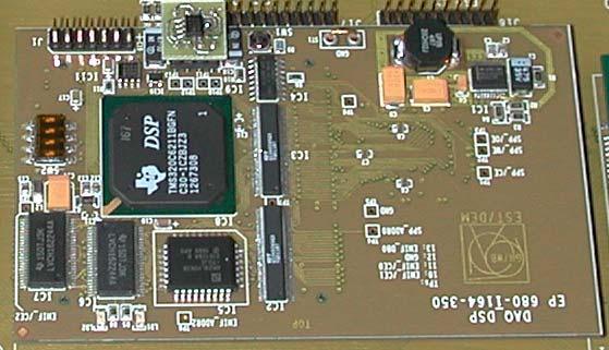
 L1 Buffer Bus Switch Evaluation card for Texas Instrument TMS320C6711 DSP 10 February 2003")
22 DSP based DAQ interface test setup FPGA used as L1B controller and data source Control interface (RB2) L1 Buffer Bus Switch Evaluation card for Texas Instrument TMS320C6711 DSP 10 February
23 L1 Buffer L1 electronics requirements for read and write: Simultaneously: Write: 36 word / 900ns Read: 36 word / 900ns (The read time can be longer for some special L1B implementations, where only L1 accepted events are read out). L1 buffer size Buffer size is 1820 events deep => 64k word deep buffer (36 word / event) Memory type options FIFO SRAM QDR/DDR 10 February
24 Comparison FIFO SRAM Simple to control since dual port and no addresses high I/O count per channel (low bandwidth) high cost, increasing depth adds high cost ($100k / 1820 events) L1 rejected events have to be read out low cost direct access from DSP possible (SBSRAM supported by DSP s) only L1 accepted events are read out Memory controller and bus arbitration necessary (single port memory) QDR/DDR very high bandwidth and therefore low I/O usage, allows high integration of the system Memory controller but no bus arbitration necessary not directly accessible by DSP 10 February
25 Comparison of two approaches to DAQ Interface DSP vs FPGA The data rate after L1 accept is 25 times lower than for the L1PPI (~25µs / event). => DSP processing is possible DSP approach Advantages Flexible for changes in algorithm since most (~90%) of the code can be written in C. Idem for special acquisition modes implementation Low cost DSP s can be used Disadvantages Some assembler is still needed. Limited bandwidth does not allow very high integration. Processing is distributed over several DSP s. 10 February
26 Comparison of two approaches to DAQ Interface DSP vs FPGA FPGA approach Advantages Only VHDL needed Processing for DAQ and L1 Pre Processor is done on only one chip, this reduces board complexity High bandwidth dual port memory can be used for easy bus arbitration Disadvantages High performance FPGA need to be used - higher cost Special mode processing also has to be implemented in VHDL 10 February
27 L1B Implementation DSP DAQ FPGA DAQ 10 February


28 Test setup Beetle setup for ST and Analog Transmission 2 RB3 setups 10 February
29 TFC Link (optical) Analog Data Links (twisted pairs) TTCrx receiver chip Vref control Clock phase Front-End Emulator Synchronization and error detection L1 Buffer FADC Ve rte x Trigg e r Preprocessor Vertex Trigger Interface RB3 Data Flow L1 Accept 40 khz L1 derandomizer Readout board Data Processing (DSP/FPGA) Area under test Control interface DAQ interface ECS link (Ethernet) DAQ Link (to NP) Link to L1 trigger (to RU) 10 February
30 RB3 testing in Lausanne Event generator on board to test readout from RB3 to L1T (S-Link to PC) DSP based DAQ card with SBSRAM L1B FPGA based card with QDR L1B Delayed clock generator for ADC s tested on FPGA FADC data read and sent to L1T (S-Link to PC) Synchronization of input data with FEM Complete read out system with FE-chip, analog transmission, FEM based synchronization, L1B, transmission via S-Link to PC. L1T Preprocessing and DAQ link 10 February

31 What s next RB3 RB4 ROB Common L1 Board VELO and VETO Inner and Outer Tracker 10 February
32 Input to L1 board VELO and VETO Analog transmission from detector to counting room FADC on L1 board 64 analog inputs (2k detector channels) SILICON TRACKER Output analog signals digitized in rad hard zone Optical link to L1 board (Serial transmission) Each ST L1 board receives data from 48 FE chips (1536 detector channels) OUTER TRACKER 32-channel OTIS TDC FE chip Optical link to L1 board (as ST -> 1536 detector channels) 10 February
33 Data flow overview Max. 24 optical inputs per board FE FE FE FE 2 or 4 RxCards 4 PP-FPGAs 1 SyncLink-FPGA 2 RO-TxCards TTCrx CC-PC FEM A-RxCard (O-RxCard) PP-FPGA L1B CC-PC TTCrx A-RxCard (O-RxCard) PP-FPGA L1B PP-FPGA L1B SyncLink-FPGA RO-Tx A-RxCard (O-RxCard) RO-Tx A-RxCard (O-RxCard) PP-FPGA L1B FEM ECS TTC L1T DAQ L1 throttle 10 February
34 Firmware framework Many common interfaces have to be implemented Blocks in red have to be developed individual for each sub-detector. Interfaces between blocks will be defined. L1B L1B L1B To PP-FPGA left and right 8 Clock Generator L1B Ctrl L1B Ctrl L1B Ctrl ECS Reset Generator Broad Cast CMD Input from RxCard Sync Sync Sync Sync Sync Sync L1T ZSupp L1A Generator L1T ZSupp 8 DAQ PPLink SyncData Generator DAQ ZSupp L1T ZSupp Throttle OR 32 L1T ZSupp 8 32 L1T ZSupp L1T PPLink L1T ZSupp PP- FPGA F I F O F I F O DAQ Link & Encapsulation L1T Link & Encapsulation ECS FIFO FIFO RO-Interface SyncLink FPGA 10 February TTCrx Throttle To RO-TxCards
35 Physical layout and its constraints Maximal card height needed for A-RxCard, not other interfaces on panel allowed. No transition module for analogue signals Front panel side 50 Pin 50 Pin 50 Pin 50 Pin A-RxCard for 16 ADC Channels A-RxCard for 16 ADC Channels A-RxCard for 16 ADC Channels A-RxCard for 16 ADC Channels Pin 200 Pin 200 Pin 200 Pin PP FPGA PP FPGA RAM RAM DDR RAM RAM PP FPGA RAM RAM PP FPGA RAM RAM RAM RAM RAM Glue Card Power 64-bit S-Link RO-TxCard SyncLink FPGA 64-bit S-Link RO-TxCard FEM TTCrx CC-PC Power Gbit Ethernet Throttle TTC Gbit Ethernet Ethernet 10 February

36 To do list Finish RB3 testing Start writing code for ROB Start a physics analysis before next seminar 10 February
Vertex Detector Electronics: ODE to ECS Interface
 Vertex Detector Electronics: ODE to ECS Interface LHCb Technical Note Issue: 1 Revision: 0 Reference: LHCb 2000-012 VELO Created: 1 February 2000 Last modified: 20 March 2000 Prepared By: Yuri Ermoline
2008 JINST 3 S Online System. Chapter System decomposition and architecture. 8.2 Data Acquisition System
 Chapter 8 Online System The task of the Online system is to ensure the transfer of data from the front-end electronics to permanent storage under known and controlled conditions. This includes not only
LHCb Online System BEAUTY-2002
 BEAUTY-2002 8th International Conference on B-Physics at Hadron machines June 17-21 2002 antiago de Compostela, Galicia (pain ) Niko Neufeld, CERN EP (for the LHCb Online Team) 1 Mission The LHCb Online
The LHCb upgrade. Outline: Present LHCb detector and trigger LHCb upgrade main drivers Overview of the sub-detector modifications Conclusions
 The LHCb upgrade Burkhard Schmidt for the LHCb Collaboration Outline: Present LHCb detector and trigger LHCb upgrade main drivers Overview of the sub-detector modifications Conclusions OT IT coverage 1.9
Electronics on the detector Mechanical constraints: Fixing the module on the PM base.
 PID meeting Mechanical implementation ti Electronics architecture SNATS upgrade proposal Christophe Beigbeder PID meeting 1 Electronics is split in two parts : - one directly mounted on the PM base receiving
Vertex Detector Electronics: ODE Pre-Prototype
 Vertex Detector Electronics: ODE Pre-Prototype User Manual Issue: 2 Revision: 1 Reference: IPHE 2000-008, LHCb 2001-057 VELO Created: 28 February 2000 Last modified: 4 May 2001 Prepared By: Yuri Ermoline
First Operational Experience from the LHCb Silicon Tracker
 First Operational Experience from the LHCb Silicon Tracker 7 th International Hiroshima Symposium on Development and Application of Semiconductor Tracking Devices The LHCb Silicon Tracker Installation
BTeV at C0. p p. Tevatron CDF. BTeV - a hadron collider B-physics experiment. Fermi National Accelerator Laboratory. Michael Wang
 BTeV Trigger BEAUTY 2003 9 th International Conference on B-Physics at Hadron Machines Oct. 14-18, 2003, Carnegie Mellon University, Fermilab (for the BTeV collaboration) Fermi National Accelerator Laboratory
RT2016 Phase-I Trigger Readout Electronics Upgrade for the ATLAS Liquid-Argon Calorimeters
 RT2016 Phase-I Trigger Readout Electronics Upgrade for the ATLAS Liquid-Argon Calorimeters Nicolas Chevillot (LAPP/CNRS-IN2P3) on behalf of the ATLAS Liquid Argon Calorimeter Group 1 Plan Context Front-end
First results from the LHCb Vertex Locator
 First results from the LHCb Vertex Locator Act 1: LHCb Intro. Act 2: Velo Design Dec. 2009 Act 3: Initial Performance Chris Parkes for LHCb VELO group Vienna Conference 2010 2 Introducing LHCb LHCb is
RPC Trigger Overview
 RPC Trigger Overview presented by Maciek Kudla, Warsaw University RPC Trigger ESR Warsaw, July 8th, 2003 RPC Trigger Task The task of RPC Muon Trigger electronics is to deliver 4 highest momentum muons
The ALICE TPC Readout Control Unit 10th Workshop on Electronics for LHC and future Experiments September 2004, BOSTON, USA
 Carmen González Gutierrez (CERN PH/ED) The ALICE TPC Readout Control Unit 10th Workshop on Electronics for LHC and future Experiments 13 17 September 2004, BOSTON, USA Outline: 9 System overview 9 Readout
Update on PRad GEMs, Readout Electronics & DAQ
 Update on PRad GEMs, Readout Electronics & DAQ Kondo Gnanvo University of Virginia, Charlottesville, VA Outline PRad GEMs update Upgrade of SRS electronics Integration into JLab DAQ system Cosmic tests
USCMS HCAL FERU: Front End Readout Unit. Drew Baden University of Maryland February 2000
 USCMS HCAL FERU: Front End Readout Unit Drew Baden University of Maryland February 2000 HCAL Front-End Readout Unit Joint effort between: University of Maryland Drew Baden (Level 3 Manager) Boston University
Stefan Koestner on behalf of the LHCb Online Group ( IEEE - Nuclear Science Symposium San Diego, Oct.
 Stefan Koestner on behalf of the LHCb Online Group (email: Stefan.Koestner@cern.ch) IEEE - Nuclear Science Symposium San Diego, Oct. 31 st 2006 Dedicated to B-physics : single arm forward spectrometer
Validation of the front-end electronics and firmware for LHCb vertex locator.
 Validation of the front-end electronics and firmware for LHCb vertex locator. Antonio Fernández Prieto Universidade de santiago de compostela, Spain E-mail: antonio.fernandez.prieto@cern.ch Pablo Vázquez
Construction of a compact DAQ-system using DSP-based VME modules
 Abstract We have developed a DSP based data-acquisition syustem(daq) system, based on the DSP. The system utilizes VME boards with one or two s. Our intension was to consturct a compact DAQ framework which
The ATLAS Level-1 Muon to Central Trigger Processor Interface
 The ATLAS Level-1 Muon to Central Processor D. Berge a, N. Ellis a, P. Farthouat a, S. Haas a, P. Klofver a, A. Krasznahorkay a,b, A. Messina a, T. Pauly a, G. Schuler a, R. Spiwoks a, T. Wengler a,c a
Production and Quality Assurance of Detector Modules for the LHCb Silicon Tracker
 Production and Quality Assurance of Detector Modules for the LHCb Silicon Tracker Olaf Steinkamp for Dmytro Volyanskyy Physik-Institut der Universität Zürich 10th ICATPP Conference on Astroparticle, Particle,
The LHCb Upgrade. LHCC open session 17 February Large Hadron Collider Physics (LHCP) Conference New York, 2-7 June 2014
 Conference New York, 2-7 June 2014") The LHCb Upgrade LHCC open session 17 February 2010 Large Hadron Collider Physics (LHCP) Conference New York, 2-7 June 2014 Andreas Schopper on behalf of Motivation LHCb is a high precision experiment
The LHCb Upgrade LHCC open session 17 February 2010 Large Hadron Collider Physics (LHCP) Conference New York, 2-7 June 2014 Andreas Schopper on behalf of Motivation LHCb is a high precision experiment
Trigger Layout and Responsibilities
 CMS EMU TRIGGER ELECTRONICS B. Paul Padley Rice University February 1999 Trigger Layout and Responsibilities Basic Requirements z Latency: < 3.2 us z Fully pipelined synchronous architecture, dead time
APV-25 based readout electronics for the SBS front GEM Tracker
 APV-25 based readout electronics for the SBS front GEM Tracker Authors: Evaristo Cisbani, Paolo Musico Date: 26/June/2014 Version: 1.0 APV-25 based readout electronics for the SBS front GEM Tracker...
The Trigger and Data Acquisition system for the NA62 experiment at CERN
 The Trigger and Data Acquisition system for the NA62 experiment at CERN M. Sozzi University of Pisa and INFN 11 th Pisa Meeting on Advanced Detectors Introduction for the unaware In year 2009 a.d. CERN
Straw Detectors for the Large Hadron Collider. Dirk Wiedner
 Straw Detectors for the Large Hadron Collider 1 Tracking with Straws Bd π π? B-Mesons properties? Charge parity symmetry violation? 2 Tracking with Straws Bd proton LHC Start 2007 π proton 14 TeV π? B-Mesons
The FTK to Level-2 Interface Card (FLIC)
") The FTK to Level-2 Interface Card (FLIC) J. Anderson, B. Auerbach, R. Blair, G. Drake, A. Kreps, J. Love, J. Proudfoot, M. Oberling, R. Wang, J. Zhang November 5th, 2015 2015 IEEE Nuclear Science Symposium
The FTK to Level-2 Interface Card (FLIC) J. Anderson, B. Auerbach, R. Blair, G. Drake, A. Kreps, J. Love, J. Proudfoot, M. Oberling, R. Wang, J. Zhang November 5th, 2015 2015 IEEE Nuclear Science Symposium
The MROD. The MDT Precision Chambers ROD. Adriaan König University of Nijmegen. 5 October nd ATLAS ROD Workshop 1
 The MROD The MDT Precision Chambers ROD Adriaan König University of Nijmegen 5 October 2000 2nd ATLAS ROD Workshop 1 Contents System Overview MROD-0 Prototype MROD-1 Prototype Performance Study FE Parameter
A flexible stand-alone testbench for facilitating system tests of the CMS Preshower
 A flexible stand-alone testbench for facilitating system tests of the CMS Preshower Paschalis Vichoudis 1,2, Serge Reynaud 1, David Barney 1, Wojciech Bialas 1, Apollo Go 3, Georgios Sidiropoulos 2, Yves
A generic firmware core to drive the Front-End GBT-SCAs for the LHCb upgrade
 A generic firmware core to drive the Front-End GBT-SCAs for the LHCb upgrade F. Alessio 1, C. Caplan, C. Gaspar 1, R. Jacobsson 1, K. Wyllie 1 1 CERN CH-, Switzerland CBPF Rio de Janeiro, Brazil Corresponding
Trigger and DAQ systems (at the LHC)
") Trigger and DAQ systems (at the LHC) Paris Sphicas CERN/PH and Univ. of Athens Summer Student Lectures August 3 2004 Introduction Level-1 Trigger DAQ Readout Switching and Event Building Control and Monitor
Trigger and DAQ systems (at the LHC) Paris Sphicas CERN/PH and Univ. of Athens Summer Student Lectures August 3 2004 Introduction Level-1 Trigger DAQ Readout Switching and Event Building Control and Monitor
Schematic. A: Overview of the Integrated Detector Readout Electronics and DAQ-System. optical Gbit link. 1GB DDR Ram.
 A: Overview of the Integrated Detector Readout Electronics and DAQ-System N s CASCADE Detector Frontend (X0) (X) (Y0) (Y) optional: CIPix- Board (T) Optical Gigabit Link CDR.0 FPGA based readout board
CMS FPGA Based Tracklet Approach for L1 Track Finding
 CMS FPGA Based Tracklet Approach for L1 Track Finding Anders Ryd (Cornell University) On behalf of the CMS Tracklet Group Presented at AWLC June 29, 2017 Anders Ryd Cornell University FPGA Based L1 Tracking
SVT detector Electronics Status
 SVT detector Electronics Status On behalf of the SVT community Mauro Citterio INFN Milano Overview: - SVT design status - F.E. chips - Electronic design - Hit rates and data volumes 1 SVT Design Detectors:
A synchronous architecture for the L0 muon trigger
 CPPM, IN2P3 CNRS et Université d Aix Marseille II A synchronous architecture for the L0 muon trigger LHCb Technical Note Issue: 1 Revision: 1 Reference: LHCb 2001 010 Created: January 23, 2001 Last modified:
New slow-control FPGA IP for GBT based system and status update of the GBT-FPGA project
 New slow-control FPGA IP for GBT based system and status update of the GBT-FPGA project 1 CERN Geneva CH-1211, Switzerland E-mail: julian.mendez@cern.ch Sophie Baron a, Pedro Vicente Leitao b CERN Geneva
CLAS12 DAQ, Trigger and Online Computing Requirements. Sergey Boyarinov Sep 25, 2017
 CLAS12 DAQ, Trigger and Online Computing Requirements Sergey Boyarinov Sep 25, 2017 Notation ECAL old EC (electromagnetic calorimeter) PCAL preshower calorimeter DC drift chamber HTCC high threshold cherenkov
Ignacy Kudla, Radomir Kupczak, Krzysztof Pozniak, Antonio Ranieri
 *** Draft *** 15/04/97 *** MK/RK/KTP/AR *** ***use color print!!!*** RPC Muon Trigger Detector Control Ignacy Kudla, Radomir Kupczak, Krzysztof Pozniak, Antonio Ranieri $Ã&06 Ã*(1(5$/ RPC Muon Trigger
SoLID GEM Detectors in US
 SoLID GEM Detectors in US Kondo Gnanvo University of Virginia SoLID Collaboration Meeting @ JLab, 05/07/2016 Outline Overview of SoLID GEM Trackers Design Optimization Large Area GEMs for PRad in Hall
MCC-DSM Specifications
 DETECTOR CHIP BUMP ELECTRONIC CHIP MCC Design Group Receiver Issue: Revision: 0.1 Reference: ATLAS ID-xx Created: 30 September 2002 Last modified: 7 October 2002 03:18 Edited By: R. Beccherle and G. Darbo
Level 0 trigger decision unit for the LHCb experiment
 Level 0 trigger decision unit for the LHCb experiment J. Laubser, H. Chanal, R. Cornat, O. Deschamps, M. Magne, P. Perret for the LHCb Collaboration Laboratoire de Physique Corpusculaire (IN2P3/CNRS),
Front End Electronics. Level 1 Trigger
 0. CMS HCAL rigger and Readout Electronics Project he overall technical coordination for the HCAL trigger and readout electronics (ri- DAS) project will be located in the Maryland HEP group, led by Drew
L1 and Subsequent Triggers
 April 8, 2003 L1 and Subsequent Triggers Abstract During the last year the scope of the L1 trigger has changed rather drastically compared to the TP. This note aims at summarising the changes, both in
The CMS Event Builder
 The CMS Event Builder Frans Meijers CERN/EP-CMD CMD on behalf of the CMS-DAQ group CHEP03, La Jolla, USA, March 24-28 28 2003 1. Introduction 2. Selected Results from the Technical Design Report R&D programme
LHC Detector Upgrades
 Su Dong SLAC Summer Institute Aug/2/2012 1 LHC is exceeding expectations in many ways Design lumi 1x10 34 Design pileup ~24 Rapid increase in luminosity Even more dramatic pileup challenge Z->µµ event
ATLAS TDAQ RoI Builder and the Level 2 Supervisor system
 ATLAS TDAQ RoI Builder and the Level 2 Supervisor system R. E. Blair 1, J. Dawson 1, G. Drake 1, W. Haberichter 1, J. Schlereth 1, M. Abolins 2, Y. Ermoline 2, B. G. Pope 2 1 Argonne National Laboratory,
PoS(EPS-HEP2017)492. Performance and recent developments of the real-time track reconstruction and alignment of the LHCb detector.
492. Performance and recent developments of the real-time track reconstruction and alignment of the LHCb detector.") Performance and recent developments of the real-time track reconstruction and alignment of the LHCb detector. CERN E-mail: agnieszka.dziurda@cern.ch he LHCb detector is a single-arm forward spectrometer
Performance and recent developments of the real-time track reconstruction and alignment of the LHCb detector. CERN E-mail: agnieszka.dziurda@cern.ch he LHCb detector is a single-arm forward spectrometer
Trigger and Data Acquisition at the Large Hadron Collider
 Trigger and Data Acquisition at the Large Hadron Collider Acknowledgments (again) This overview talk would not exist without the help of many colleagues and all the material available online I wish to
Prototyping NGC. First Light. PICNIC Array Image of ESO Messenger Front Page
 Prototyping NGC First Light PICNIC Array Image of ESO Messenger Front Page Introduction and Key Points Constructed is a modular system with : A Back-End as 64 Bit PCI Master/Slave Interface A basic Front-end
EMU FED. --- Crate and Electronics. ESR, CERN, November B. Bylsma, S. Durkin, Jason Gilmore, Jianhui Gu, T.Y. Ling. The Ohio State University
 EMU FED --- Crate and Electronics B. Bylsma, S. Durkin, Jason Gilmore, Jianhui Gu, T.Y. Ling The Ohio State University ESR, CERN, November 2004 EMU FED Design EMU FED: Outline FED Crate & Custom Backplane
Data Acquisition in Particle Physics Experiments. Ing. Giuseppe De Robertis INFN Sez. Di Bari
 Data Acquisition in Particle Physics Experiments Ing. Giuseppe De Robertis INFN Sez. Di Bari Outline DAQ systems Theory of operation Case of a large experiment (CMS) Example of readout GEM detectors for
BES-III off-detector readout electronics for the GEM detector: an update
 BES-III off-detector readout electronics for the GEM detector: an update The CGEM off-detector collaboration ( INFN/Univ. FE, INFN LNF, Univ. Uppsala ) 1 Outline Reminder Update on development status Off-detector
SoLID GEM Detectors in US
 SoLID GEM Detectors in US Kondo Gnanvo University of Virginia SoLID Collaboration Meeting @ JLab, 08/26/2016 Outline Design Optimization U-V strips readout design Large GEMs for PRad in Hall B Requirements
Field Program mable Gate Arrays
 Field Program mable Gate Arrays M andakini Patil E H E P g r o u p D H E P T I F R SERC school NISER, Bhubaneshwar Nov 7-27 2017 Outline Digital electronics Short history of programmable logic devices
Technical Information Manual
 Technical Information Manual Revision n. 3 28 August 2002 MOD. V550 / V550 B MOD. V550 A / V550 AB 2 CHANNEL C-RAMS CAEN will repair or replace any product within the guarantee period if the Guarantor
Using the SPECS in LHCb
 LHCb 2003-005 DAQ 21 January 2003 Using the in LHCb Dominique Breton, Daniel Charlet Laboratoire de l Accélérateur Linéaire - Orsay ABSTRACT This document attempts to describe how to use the in LHCb. The
Track-Finder Test Results and VME Backplane R&D. D.Acosta University of Florida
 Track-Finder Test Results and VME Backplane R&D D.Acosta University of Florida 1 Technical Design Report Trigger TDR is completed! A large amount effort went not only into the 630 pages, but into CSC Track-Finder
ALIBAVA: A portable readout system for silicon microstrip sensors
 ALIBAVA: A portable readout system for silicon microstrip sensors Marco-Hernández, R. a, Bernabeu, J. a, Casse, G. b, García, C. a, Greenall, A. b, Lacasta, C. a, Lozano, M. c, Martí i García, S. a, Martinez,
Modules and Front-End Electronics Developments for the ATLAS ITk Strips Upgrade
 Modules and Front-End Electronics Developments for the ATLAS ITk Strips Upgrade Carlos García Argos, on behalf of the ATLAS ITk Collaboration University of Freiburg International Conference on Technology
NEMbox / NIMbox Programmable NIM Module
 NEMbox / NIMbox Programmable NIM Module Request Quote NEMbox / NIMbox Programmable NIM Module NEMbox (Nuclear Electronics Miniature Box) is a programmable Logic / DAQ module, powered either in a NIM crate
CSC Trigger Motherboard
 CSC Trigger Motherboard Functions of TMB Tests: Performance at summer 2003 test beam Radiation, magnetic fields, etc. Plans for TMB production and testing 1 Cathode LCT CSC Trigger Requirements Identify
Detector Control LHC
 Detector Control Systems @ LHC Matthias Richter Department of Physics, University of Oslo IRTG Lecture week Autumn 2012 Oct 18 2012 M. Richter (UiO) DCS @ LHC Oct 09 2012 1 / 39 Detectors in High Energy
Readout Systems. Liquid Argon TPC Analog multiplexed ASICs SiPM arrays. CAEN 2016 / 2017 Product Catalog
 Readout Systems Liquid Argon TPC Analog multiplexed ASICs SiPM arrays CAEN 2016 / 2017 Product Catalog 192 Readout Systems SY2791 Liquid Argon TPC Readout System The SY2791 is a complete detector readout
The Read-Out Driver (ROD) for the ATLAS Liquid Argon Calorimeters
 for the ATLAS Liquid Argon Calorimeters") The Read-Out Driver (ROD) for the ATLAS Liquid Argon Calorimeters Outline The read-out architecture The front-end boards The front-end links The read-out driver (ROD) modules design considerations prototype
The Read-Out Driver (ROD) for the ATLAS Liquid Argon Calorimeters Outline The read-out architecture The front-end boards The front-end links The read-out driver (ROD) modules design considerations prototype
Overview of SVT DAQ Upgrades. Per Hansson Ryan Herbst Benjamin Reese
 Overview of SVT DAQ Upgrades Per Hansson Ryan Herbst Benjamin Reese 1 SVT DAQ Requirements and Constraints Basic requirements for the SVT DAQ Continuous readout of 23 040 channels Low noise (S/N>20 to
Alternative Ideas for the CALICE Back-End System
 Alternative Ideas for the CALICE Back-End System Matthew Warren and Gordon Crone University College London 5 February 2002 5 Feb 2002 Alternative Ideas for the CALICE Backend System 1 Concept Based on
GLAST Silicon Microstrip Tracker Status
 R.P. Johnson Santa Cruz Institute for Particle Physics University of California at Santa Cruz Mechanical Design Detector Procurement Work list for the Prototype Tracker Construction. ASIC Development Hybrids
Electronics, Trigger and Data Acquisition part 3
 Electronics, Trigger and Data Acquisition part 3 Summer Student Programme 2016, CERN Roberto Ferrari Instituto Nazionale di Fisica Nucleare roberto.ferrari@pv.infn.it Event Building 2 Two Philosophies
TOF Electronics. J. Schambach University of Texas Review, BNL, 2 Aug 2007
 TOF Electronics J. Schambach University of Texas Review, BNL, 2 Aug 2007 1 Outline Electronics Overview Trigger & DAQ Interfaces Board Status, Tests & Plans 2 Electronics for One Side 3 Tray Level Electronics
CLAS12 DAQ & Trigger Status and Timeline. Sergey Boyarinov Oct 3, 2017
 CLAS12 DAQ & Trigger Status and Timeline Sergey Boyarinov Oct 3, 2017 Notation ECAL old EC (electromagnetic calorimeter) PCAL preshower calorimeter DC drift chamber HTCC high threshold cherenkov counter
An adapted SCTA for the readout of the Si strip VErtex LOcator of LHCb.
 : Adapted scta for LHCB Vertex locator. An adapted SCTA for the readout of the Si strip VErtex LOcator of LHCb. (CERN) F. Vinci dos Santos (CERN/RIO) E. Sexauer(Heidelberg) IVth international meeting on
CMS Trigger/DAQ HCAL FERU System
 CMS Trigger/DAQ HCAL FERU System Drew Baden University of Maryland October 2000 http://macdrew.physics.umd.edu/cms/ Honest assessment: About 3 months behind schedule. TRIDAS Overall Project Timelines Expected
MiniDAQ1 A COMPACT DATA ACQUISITION SYSTEM FOR GBT READOUT OVER 10G ETHERNET 22/05/2017 TIPP PAOLO DURANTE - MINIDAQ1 1
 MiniDAQ1 A COMPACT DATA ACQUISITION SYSTEM FOR GBT READOUT OVER 10G ETHERNET 22/05/2017 TIPP 2017 - PAOLO DURANTE - MINIDAQ1 1 Overview LHCb upgrade Optical frontend readout Slow control implementation
A generic firmware core to drive the Front-End GBT-SCAs for the LHCb upgrade
 Journal of Instrumentation OPEN ACCESS A generic firmware core to drive the Front-End GBT-SCAs for the LHCb upgrade Recent citations - The Versatile Link Demo Board (VLDB) R. Martín Lesma et al To cite
The GTPC Package: Tracking and Analysis Software for GEM TPCs
 The GTPC Package: Tracking and Analysis Software for GEM TPCs Linear Collider TPC R&D Meeting LBNL, Berkeley, California (USA) 18-19 October, 003 Steffen Kappler Institut für Experimentelle Kernphysik,
S-LINK: A Prototype of the ATLAS Read-out Link
 : A Prototype of the ATLAS Read-out Link Erik van der Bij, Robert McLaren, Zoltán Meggyesi EP-Division CERN, CH-1211 Geneva 23 Abstract The ATLAS data acquisition system needs over 1500 read-out links
D Demonstration of disturbance recording functions for PQ monitoring
 D6.3.7. Demonstration of disturbance recording functions for PQ monitoring Final Report March, 2013 M.Sc. Bashir Ahmed Siddiqui Dr. Pertti Pakonen 1. Introduction The OMAP-L138 C6-Integra DSP+ARM processor
Signal Conversion in a Modular Open Standard Form Factor. CASPER Workshop August 2017 Saeed Karamooz, VadaTech
 Signal Conversion in a Modular Open Standard Form Factor CASPER Workshop August 2017 Saeed Karamooz, VadaTech At VadaTech we are technology leaders First-to-market silicon Continuous innovation Open systems
Using the FADC250 Module (V1C - 5/5/14)
") Using the FADC250 Module (V1C - 5/5/14) 1.1 Controlling the Module Communication with the module is by standard VME bus protocols. All registers and memory locations are defined to be 4-byte entities.
Using the FADC250 Module (V1C - 5/5/14) 1.1 Controlling the Module Communication with the module is by standard VME bus protocols. All registers and memory locations are defined to be 4-byte entities.
DTTF muon sorting: Wedge Sorter and Barrel Sorter
 DTTF muon sorting: Wedge Sorter and Barrel Sorter 1 BS, it sorts the 4 best tracks out of max 24 tracks coming from the 12 WS of barrel Vienna Bologna PHTF 72 x Vienna Bologna Padova 12 WS, each one sorts
1 MHz Readout. LHCb Technical Note. Artur Barczyk, Guido Haefeli, Richard Jacobsson, Beat Jost, and Niko Neufeld. Revision: 1.0
 1 MHz Readout LHCb Technical Note Issue: Final Revision: 1.0 Reference: LHCb 2005 62 Created: 9 March, 2005 Last modified: 7 September 2005 Prepared By: Artur Barczyk, Guido Haefeli, Richard Jacobsson,
Implementation of on-line data reduction algorithms in the CMS Endcap Preshower Data Concentrator Cards
 Journal of Instrumentation OPEN ACCESS Implementation of on-line data reduction algorithms in the CMS Endcap Preshower Data Concentrator Cards To cite this article: D Barney et al Related content - Prototype
A Fast Ethernet Tester Using FPGAs and Handel-C
 A Fast Ethernet Tester Using FPGAs and Handel-C R. Beuran, R.W. Dobinson, S. Haas, M.J. LeVine, J. Lokier, B. Martin, C. Meirosu Copyright 2000 OPNET Technologies, Inc. The Large Hadron Collider at CERN
FPGA based Sampling ADC for Crystal Barrel
 FPGA based Sampling ADC for Crystal Barrel Johannes Müllers for the CBELSA/TAPS collaboration Rheinische Friedrich-Wilhelms-Universität Bonn CBELSA/TAPS Experiment (Bonn) Investigation of the baryon excitation
GCU ARCHITECTURE PROPOSAL
 GCU ARCHITECTURE PROPOSAL M. Bellato, R. Brugnera, F. Dal Corso, S. Dusini, A. Garfagnini, R. Isocrate, I. Lippi, G. Meng, D. Pedretti INFN and University of Padova GCU ARCHITECTURE PROPOSAL LCU DCS VD
HCAL TPG and Readout
 HCAL TPG and Readout CMS HCAL Readout Status CERN Tullio Grassi, Drew Baden University of Maryland Jim Rohlf Boston University CMS/CERN. Nov, 2001 HCAL TriDAS 1 CMS TriDAS Architecture Data from CMS FE
On-board PCs for interfacing front-end electronics
 On-board PCs for interfacing front-end electronics JCOP team meeting April 10, 2002 Niko Neufeld CERN/EP 1 Controlling Boards The traditional approach Ethernet Parallel Bus (VME, Fastbus, ) Control Station
Improving Packet Processing Performance of a Memory- Bounded Application
 Improving Packet Processing Performance of a Memory- Bounded Application Jörn Schumacher CERN / University of Paderborn, Germany jorn.schumacher@cern.ch On behalf of the ATLAS FELIX Developer Team LHCb
Scintillator-strip Plane Electronics
 Scintillator-strip Plane Electronics Mani Tripathi Britt Holbrook (Engineer) Juan Lizarazo (Grad student) Peter Marleau (Grad student) Tiffany Landry (Junior Specialist) Cherie Williams (Undergrad student)
The Intelligent FPGA Data Acquisition
 The Intelligent FPGA Data Acquisition Dominic Gaisbauer, Stefan Huber, Igor Konorov, Dmytro Levit, Prof. Dr. Stephan Paul, Dominik Steffen d.gaisbauer@tum.de Technische Universität München Institute for
ATLANTIS - a modular, hybrid FPGA/CPU processor for the ATLAS. University of Mannheim, B6, 26, Mannheim, Germany
 ATLANTIS - a modular, hybrid FPGA/CPU processor for the ATLAS Readout Systems A. Kugel, Ch. Hinkelbein, R. Manner, M. Muller, H. Singpiel University of Mannheim, B6, 26, 68131 Mannheim, Germany fkugel,
TORCH: A large-area detector for precision time-of-flight measurements at LHCb
 TORCH: A large-area detector for precision time-of-flight measurements at LHCb Neville Harnew University of Oxford ON BEHALF OF THE LHCb RICH/TORCH COLLABORATION Outline The LHCb upgrade TORCH concept
ALIBAVA: A portable readout system for silicon microstrip sensors
 ALIBAVA: A portable readout system for silicon microstrip sensors Marco-Hernández, R. a, Bernabeu, J. a, Casse, G. b, García, C. a, Greenall, A. b, Lacasta, C. a, Lozano, M. c, Martí i García, S. a, Martinez,
Integrated CMOS sensor technologies for the CLIC tracker
 Integrated CMOS sensor technologies for the CLIC tracker Magdalena Munker (CERN, University of Bonn) On behalf of the collaboration International Conference on Technology and Instrumentation in Particle
Istituto Nazionale di Fisica Nucleare A FADC based DAQ system for Double Beta Decay Experiments
 Istituto Nazionale di Fisica Nucleare A FADC based DAQ system for Double Beta Decay Experiments Description of the DAQ system PC control and Data analysis Future developments 1 Acquisition System for Pulse
GLAST. Prototype Tracker Tower Construction Status
 Prototype Tracker Tower Construction Status June 22, 1999 R.P. Johnson Santa Cruz Institute for Particle Physics University of California at Santa Cruz 1 1 11 2 3 5 4 Prototype Tracker Tower Configuration
IBM Network Processor, Development Environment and LHCb Software
 IBM Network Processor, Development Environment and LHCb Software LHCb Readout Unit Internal Review July 24 th 2001 Niko Neufeld, CERN 1 Outline IBM NP4GS3 Architecture A Readout Unit based on the NP4GS3
PSEC-4: Review of Architecture, etc. Eric Oberla 27-oct-2012
 PSEC-4: Review of Architecture, etc. Eric Oberla 27-oct-2012 PSEC-4 ASIC: design specs LAPPD Collaboration Designed to sample & digitize fast pulses (MCPs): Sampling rate capability > 10GSa/s Analog bandwidth
LVL1 e/γ RoI Builder Prototype
 LVL e/γ RoI Builder Prototype RoI / s matching and zero suppression Receiver RoI VME Receiver RoI Control Receiver RoI S-Link Interface Receiver Output - LVL / Supervisor RoI Builder discussion - Verilog/VHDL
Development of LYSO Detector Modules for an EDM Polarimeter at COSY. for the JEDI Collaboration
 Mitglied der Helmholtz-Gemeinschaft Development of LYSO Detector Modules for an EDM Polarimeter at COSY for the JEDI Collaboration February 28, 2018 DPG Spring Meeting, PhD @ SMART EDM_Lab, TSU, Georgia
Development and test of a versatile DAQ system based on the ATCA standard
 Development and test of a versatile DAQ system based on the ATCA standard M.Bianco, a P.J.Loesel, b S.Martoiu, c, ad and A.Zibell e a CERN PH Department, Geneve, Switzerland b Ludwig-Maximilians-Univ.
Upgrading the ATLAS Tile Calorimeter electronics
 ITIM Upgrading the ATLAS Tile Calorimeter electronics Gabriel Popeneciu, on behalf of the ATLAS Tile Calorimeter System INCDTIM Cluj Napoca, Romania Gabriel Popeneciu PANIC 2014, Hamburg 26th August 2014