An adapted SCTA for the readout of the Si strip VErtex LOcator of LHCb.
|
|
|
- Lesley King
- 5 years ago
- Views:
Transcription
1 : Adapted scta for LHCB Vertex locator. An adapted SCTA for the readout of the Si strip VErtex LOcator of LHCb. (CERN) F. Vinci dos Santos (CERN/RIO) E. Sexauer(Heidelberg) IVth international meeting on Frontend electronics for high resolution tracking detectors. Perugia 00
2 : Adapted scta for LHCB Vertex locator. Outline: I. Introduction to LHCb and VErtex LOcator (VELO). II. SCTA_VELO requirements. III. Analog signal chain. IV. Readout controller. V. Pipeline and control. VI. Programming interface. IVth international meeting on Frontend electronics for high resolution tracking detectors. Perugia 00

3 LHCb B-meson events

4 Geometry of VErtex LOcator. ~ 25 stations stations= r and phi sensor ~ 30mm spacing small overlap separation during injection

5 R measuring sensor 8mm r pitch 25 um ~ thickness 200 um : 1MIP ~ 2.7 fc 2048 strips /sensor capacitance 10~25 pf pitch 18 um 45mm Phi measuring sensor.
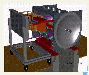

6 Mechanical support Vacuum vessel
7 : Adapted scta for LHCB Vertex locator. II. Requirements: SCTA_VELO pipeline delay 4 us. event readout > 1 MHz. deadtimeless (no restriction on trigger-interva). 16 event buffer. minimize spillover (=value 25 ns after peak). readback of configuration bits. SCTA2 ~ 3 us ~ 0.03 MHz. > 3 8 ~ 20% no IVth international meeting on Frontend electronics for high resolution tracking detectors. Perugia 00
8 : Adapted scta for LHCB Vertex locator. III. Analog signal chain (scta_velo) Preamplifier & Shaper Pipeline Readout Sample/ hold Multiplexer x4 x184 x32 Pointers bias Encoder/decoder Fifo (16x8) Readout sequencer RST TRG CLK Serial IVth international meeting on Frontend electronics for high resolution tracking detectors. Perugia 00
9 : Adapted scta for LHCB Vertex locator. Preamplifier and shaper analog blocks (SCTA3). Preamplifier Shaper stage1 stage2 stage3 x1 gain: 3.6 mv/fc ~ 4 V/V ~ 4 V/V ~1 (>1000 V/V) freq: ~ 1/f ~ 1/f 2 ~f ~ 1/f 2 ~f =57 mv/fc =CR 2 -RC 5 IVth international meeting on Frontend electronics for high resolution tracking detectors. Perugia 00
10 Pulse shapes in preamplifier & shaper for -10fC input pulse (scta3). shaper 2-stage : 56 mv/fc shaper 1-stage: 14,7 mv/fc transimpedance : 3.6 mv/fc nanoscconds
11 Frequency response of preampifier and shaper stages. ~f 2 ~f -5 ~f -1 ~f ~f ~f -2 ~f -2
12 : Adapted scta for LHCB Vertex locator. modifications SCTA_VELO : - operate at Vdd= 5V and Vref= 2V. - 40% gain reduction (stage2) : ~30 mv/fc obtain symmetric 20/-20 fc range. IVth international meeting on Frontend electronics for high resolution tracking detectors. Perugia 00
13 Gain reduction in SCTA_VELO. (irradiated, slow conditions)
14 Linear signal range in SCTA_VELO. (irradiated, slow conditions) -20 to 20 fc (4fC step) spill-over < 10% 25 ns
15 Comparison 4fC and -4-4fC shaper response. output. (irradiated, slow conditions) 14% undershoot
16 : Adapted scta for LHCB Vertex locator. Pulse peak-voltage storage. Preamplifier & Shaper Pipeline x184-50% load increase on output : not significant in scta3. -worst case simulation ok. IVth international meeting on Frontend electronics for high resolution tracking detectors. Perugia 00
17 Comparison of shaper output with extended pipeline. (128 to 184 cells)
18 Peak voltage storage of -20fC pulse (irradiated, slow conditions)
19 Peak voltage storage of 20fC pulse (irradiated, slow conditions)
20 : Adapted scta for LHCB Vertex locator. Stored charge readout and sample/hold. Pipeline Readout C r Sample/ hold C s x184 stray C S/H sample time must < 200ns. (for 1 MHz readout). direct transfer of C s to C S/H too slow. -> 2 phase readout : a. C storage to C r b. C r to C S/H IVth international meeting on Frontend electronics for high resolution tracking detectors. Perugia 00
21 : Adapted scta for LHCB Vertex locator. 1MHz readout: phase a: phase b: evt n 1000 ns evt n ns header data header data evt n ns evt n ns plenty of time during header available of event. sample time too short for full settling: (because 50% increased C stray ~ 10* C storage ) -increase transconductance of amplifier, -and reduce C h. -safety : sample time can be programmed 100ns - 500ns IVth international meeting on Frontend electronics for high resolution tracking detectors. Perugia 00
22 Charge readout from memory. (phase a) (irradiated, slow conditions)
23 Sample/hold on readout capacitor. (phase b) (irradiated, slow conditions, 100ns gate)
24 Sample/hold on readout capacitor. (phase b) (un-irradiated, typ. conditions, 100 ns gate)
25 Sample/hold on readout capacitor. (phase b) (irradiated, slow conditions, 150 ns gate) -20 fc
26 : Adapted scta for LHCB Vertex locator. Output multiplexer. Sample/ hold Multiplexer x32 - to read Mhz < 1000 ns. -> split 128:1 in 4 parallel 32:1 multiplexers. - splitting reduces settling times. - power dissipation x4. IVth international meeting on Frontend electronics for high resolution tracking detectors. Perugia 00
27 Multiplexer: -20 fc after 0 fc channel. (irrad., slow)
28 Multiplexer: 0 fc after -20 fc channel. (irrad., slow)
29 SCTA_VELO: Adapted scta for LHCB Vertex locator. IV. Readout controller. - new design and simplified (no chip pairing). Readout block diagram Clear state-diagram Cstore read Cf Chold hold Mux 32:1 m_out4 m_out3 m_out2 m_out1 vref reset skip cell Unlock Lock Decoder Read_enable Decode_enable Fifo_read le Start E n ab Rclk reset FIFO empty FIFO Fifo_write Fifo_empty Readout controller phase a Fifo_full Trigger phase b & start mux reset l_reset Ful L1_reset ay d_del hol IVth international meeting on Frontend electronics for high resolution tracking detectors. Perugia 00
30 : Adapted scta for LHCB Vertex locator. V. Pipeline and controller. -extension of length: 4 us latency -> 160 cells. derandomizer -> 16 cells. special (trigger burst) condition -> 6 cells. dummy cell -> 2 cells. total = 184 cells -programmable latency. -reset independent of readout. -FIFO has been extended to 16 depth. -control signal dsitribution (long lines) verified. IVth international meeting on Frontend electronics for high resolution tracking detectors. Perugia 00
31 : Adapted scta for LHCB Vertex locator. VI. I2C interface. -readback of static configuration bits. (SEU check) -need addressing capability on multichip hybrid. -standard protocol. -plan to reuse existing design (TTCrx). -sufficient area available? IVth international meeting on Frontend electronics for high resolution tracking detectors. Perugia 00
32 : Adapted scta for LHCB Vertex locator. Conclusion. SCTA_VELO: - no fundamental change to SCTA3 analog signal path, to obtain : 1MHz event readout (16 eventbuffer), deadtimeless, 4us pipeline operation - peripheral enhancements: programmable latency, independent pipeline and readout reset, read back of configuration. IVth international meeting on Frontend electronics for high resolution tracking detectors. Perugia 00
IEEE Proof Web Version
 IEEE TRANSACTIONS ON NUCLEAR SCIENCE, VOL. 56, NO. 3, JUNE 2009 1 A Portable Readout System for Microstrip Silicon Sensors (ALIBAVA) Ricardo Marco-Hernández and ALIBAVA COLLABORATION Abstract A readout
ALIBAVA: A portable readout system for silicon microstrip sensors
 ALIBAVA: A portable readout system for silicon microstrip sensors Marco-Hernández, R. a, Bernabeu, J. a, Casse, G. b, García, C. a, Greenall, A. b, Lacasta, C. a, Lozano, M. c, Martí i García, S. a, Martinez,
ALIBAVA: A portable readout system for silicon microstrip sensors
 ALIBAVA: A portable readout system for silicon microstrip sensors Marco-Hernández, R. a, Bernabeu, J. a, Casse, G. b, García, C. a, Greenall, A. b, Lacasta, C. a, Lozano, M. c, Martí i García, S. a, Martinez,
Electronics on the detector Mechanical constraints: Fixing the module on the PM base.
 PID meeting Mechanical implementation ti Electronics architecture SNATS upgrade proposal Christophe Beigbeder PID meeting 1 Electronics is split in two parts : - one directly mounted on the PM base receiving
Conceptual Design of Front-End Readout Electronics for the GLAST Silicon-Strip Tracker
 Introduction Conceptual Design of Front-End Readout Electronics for the GLAST Silicon-Strip Tracker R.P. Johnson, SCIPP Draft: November 13, 1998 This is a conceptual design for the GLAST silicon-strip
Modules and Front-End Electronics Developments for the ATLAS ITk Strips Upgrade
 Modules and Front-End Electronics Developments for the ATLAS ITk Strips Upgrade Carlos García Argos, on behalf of the ATLAS ITk Collaboration University of Freiburg International Conference on Technology
A flexible stand-alone testbench for characterizing the front-end electronics for the CMS Preshower detector under LHC-like timing conditions
 A flexible stand-alone testbench for characterizing the front-end electronics for the CMS Preshower detector under LHC-like timing conditions Paul Aspell 1, David Barney 1, Yves Beaumont 1, Suhas Borkar
PSEC-4: Review of Architecture, etc. Eric Oberla 27-oct-2012
 PSEC-4: Review of Architecture, etc. Eric Oberla 27-oct-2012 PSEC-4 ASIC: design specs LAPPD Collaboration Designed to sample & digitize fast pulses (MCPs): Sampling rate capability > 10GSa/s Analog bandwidth
Velo readout board RB3. Common L1 board (ROB)
") Velo readout board RB3 Testing... Common L1 board (ROB) Specifying Federica Legger 10 February 2003 1 Summary LHCb Detectors Online (Trigger, DAQ) VELO (detector and Readout chain) L1 electronics for VELO
Velo readout board RB3 Testing... Common L1 board (ROB) Specifying Federica Legger 10 February 2003 1 Summary LHCb Detectors Online (Trigger, DAQ) VELO (detector and Readout chain) L1 electronics for VELO
EECS150 - Digital Design Lecture 17 Memory 2
 EECS150 - Digital Design Lecture 17 Memory 2 October 22, 2002 John Wawrzynek Fall 2002 EECS150 Lec17-mem2 Page 1 SDRAM Recap General Characteristics Optimized for high density and therefore low cost/bit
HPS128-LT-S Hybrid pyroelectric linear array with 128 responsive elements and integrated CMOS multiplexer
 HPS128-LT-S Hybrid pyroelectric linear array with 128 responsive elements and integrated CMOS multiplexer Description The pyroelectric linear array 128-LT is a hybrid detector with 128 responsive elements
Part 1: Results from SPADIC 0.3
 Part 1: Results from SPADIC 0.3 Tim Armbruster tim.armbruster@ziti.uni-heidelberg.de 17th CBM CM, Dresden Schaltungstechnik Schaltungstechnik und und April 2011 Visit http://www.spadic.uni-hd.de 1. Reminder:
Nevis ADC Design. Jaroslav Bán. Columbia University. June 4, LAr ADC Review. LAr ADC Review. Jaroslav Bán
 Nevis ADC Design Columbia University June 4, 2014 Outline The goals of the project Introductory remarks The road toward the design Components developed in Nevis09, Nevis10 and Nevis12 Nevis13 chip Architecture
THE latest generation of microprocessors uses a combination
 1254 IEEE JOURNAL OF SOLID-STATE CIRCUITS, VOL. 30, NO. 11, NOVEMBER 1995 A 14-Port 3.8-ns 116-Word 64-b Read-Renaming Register File Creigton Asato Abstract A 116-word by 64-b register file for a 154 MHz
Vertex Detector Electronics: ODE Pre-Prototype
 Vertex Detector Electronics: ODE Pre-Prototype User Manual Issue: 2 Revision: 1 Reference: IPHE 2000-008, LHCb 2001-057 VELO Created: 28 February 2000 Last modified: 4 May 2001 Prepared By: Yuri Ermoline
Readout Systems. Liquid Argon TPC Analog multiplexed ASICs SiPM arrays. CAEN 2016 / 2017 Product Catalog
 Readout Systems Liquid Argon TPC Analog multiplexed ASICs SiPM arrays CAEN 2016 / 2017 Product Catalog 192 Readout Systems SY2791 Liquid Argon TPC Readout System The SY2791 is a complete detector readout
Vertex Detector Electronics: ODE to ECS Interface
 Vertex Detector Electronics: ODE to ECS Interface LHCb Technical Note Issue: 1 Revision: 0 Reference: LHCb 2000-012 VELO Created: 1 February 2000 Last modified: 20 March 2000 Prepared By: Yuri Ermoline
FLAME, a new readout ASIC for the LumiCal detector
 FLAME, a new readout ASIC for the LumiCal detector Jakub Moroń AGH-UST M. Firlej, T. Fiutowski, M. Idzik, K. Świentek Students: Sz. Bugiel, R. Dasgupta, M. Kuczyńska, J. Murdzek On behalf of FCAL Collaboration
PART TOP VIEW ADDR2 ADDR3 ADDR4 SELECT S/H CONFIG V L DGND V SS AGND IN N.C. Maxim Integrated Products 1
 9-674; Rev ; 4/ 32-Channel Sample/Hold Amplifier General Description The MAX568 contains 32 sample/hold amplifiers and four -of-8 multiplexers. The logic controlling the muxes and sample/hold amplifiers
Lecture 13: SRAM. Slides courtesy of Deming Chen. Slides based on the initial set from David Harris. 4th Ed.
 Lecture 13: SRAM Slides courtesy of Deming Chen Slides based on the initial set from David Harris CMOS VLSI Design Outline Memory Arrays SRAM Architecture SRAM Cell Decoders Column Circuitry Multiple Ports
Memory. Outline. ECEN454 Digital Integrated Circuit Design. Memory Arrays. SRAM Architecture DRAM. Serial Access Memories ROM
 ECEN454 Digital Integrated Circuit Design Memory ECEN 454 Memory Arrays SRAM Architecture SRAM Cell Decoders Column Circuitry Multiple Ports DRAM Outline Serial Access Memories ROM ECEN 454 12.2 1 Memory
The System of Readout Boards for ALICE TRD
 PRESENTATION The System of Readout Boards for ALICE TRD Dr. Ivan Rusanov Physics Institute, Uni - Heidelberg ALICE TRD: Charge Sensitive Preamplifier (PASA Measurements - Dr. Ivan Rusanov; PI, Uni-Heidelberg)
Lecture 11 SRAM Zhuo Feng. Z. Feng MTU EE4800 CMOS Digital IC Design & Analysis 2010
 EE4800 CMOS Digital IC Design & Analysis Lecture 11 SRAM Zhuo Feng 11.1 Memory Arrays SRAM Architecture SRAM Cell Decoders Column Circuitryit Multiple Ports Outline Serial Access Memories 11.2 Memory Arrays
PART TOP VIEW ADDR2 ADDR3 ADDR4 SELECT S/H CONFIG V L DGND V SS AGND IN CH. Maxim Integrated Products 1
 9-675; Rev ; 4/ 32-Channel Sample/Hold Amplifier General Description The MAX567 contains 32 sample-and-hold amplifiers driven by a single multiplexed input. The control logic addressing the outputs is
Schematic. A: Overview of the Integrated Detector Readout Electronics and DAQ-System. optical Gbit link. 1GB DDR Ram.
 A: Overview of the Integrated Detector Readout Electronics and DAQ-System N s CASCADE Detector Frontend (X0) (X) (Y0) (Y) optional: CIPix- Board (T) Optical Gigabit Link CDR.0 FPGA based readout board
Detector R&D at the LCFI Collaboration
 LCFI Overview Detector R&D at the LCFI Collaboration (Bristol U, Oxford U, Lancaster U, Liverpool U, RAL) Konstantin Stefanov on behalf of the LCFI collaboration LCWS2005, Stanford, 18-22 March 2005 Introduction
SRAM. Introduction. Digital IC
 SRAM Introduction Outline Memory Arrays SRAM Architecture SRAM Cell Decoders Column Circuitry Multiple Ports Serial Access Memories Memory Arrays Memory Arrays Random Access Memory Serial Access Memory
First Operational Experience from the LHCb Silicon Tracker
 First Operational Experience from the LHCb Silicon Tracker 7 th International Hiroshima Symposium on Development and Application of Semiconductor Tracking Devices The LHCb Silicon Tracker Installation
FLIR ISC9705 LOW STANDARD 320
 FLIR ISC9705 LOW STANDARD 320 400-9705-09 Version 1.3 7/31/02 1.0 Features 320 X 256 ixels Snapshot Mode on N Input olarity 18 Million Electron Well Capacity Flexible Integration Control Integrate-While-Read
C ELEMENTS LINEAR IMAGE SENSOR DATA SHEET
 March 2008 4000 ELEMENTS LINEAR IMAGE SENSOR DATA SHEET Website: http://www.csensor.com / E-mail : sales@csensor.com March 06, 2007 Page 1 Contents 1. General description ------------------------------------------------------
Front-End Electronics Configuration System for CMS. Philippe Gras CERN - University of Karlsruhe
 Front-End Electronics Configuration System for CMS Philippe Gras CERN - University of Karlsruhe Outline Introduction Tracker electronics parameters Tracker beam test DCS overview Electronics configuration
COMPUTER ARCHITECTURES
 COMPUTER ARCHITECTURES Random Access Memory Technologies Gábor Horváth BUTE Department of Networked Systems and Services ghorvath@hit.bme.hu Budapest, 2019. 02. 24. Department of Networked Systems and
Endcap Modules for the ATLAS SemiConductor Tracker
 Endcap Modules for the ATLAS SemiConductor Tracker RD3, Firenze, September 29 th, 23 Richard Nisius (MPI Munich) nisius@mppmu.mpg.de (For the ATLAS-SCT Collaboration) The plan of this presentation Introduction
A Configurable Radiation Tolerant Dual-Ported Static RAM macro, designed in a 0.25 µm CMOS technology for applications in the LHC environment.
 A Configurable Radiation Tolerant Dual-Ported Static RAM macro, designed in a 0.25 µm CMOS technology for applications in the LHC environment. 8th Workshop on Electronics for LHC Experiments 9-13 Sept.
Introduction to Semiconductor Memory Dr. Lynn Fuller Webpage:
 ROCHESTER INSTITUTE OF TECHNOLOGY MICROELECTRONIC ENGINEERING Introduction to Semiconductor Memory Webpage: http://people.rit.edu/lffeee 82 Lomb Memorial Drive Rochester, NY 14623-5604 Tel (585) 475-2035
Introduction to CMOS VLSI Design Lecture 13: SRAM
 Introduction to CMOS VLSI Design Lecture 13: SRAM David Harris Harvey Mudd College Spring 2004 1 Outline Memory Arrays SRAM Architecture SRAM Cell Decoders Column Circuitry Multiple Ports Serial Access
Update on PRad GEMs, Readout Electronics & DAQ
 Update on PRad GEMs, Readout Electronics & DAQ Kondo Gnanvo University of Virginia, Charlottesville, VA Outline PRad GEMs update Upgrade of SRS electronics Integration into JLab DAQ system Cosmic tests
Infineon HYB39S128160CT M SDRAM Circuit Analysis
 September 8, 2004 Infineon HYB39S128160CT-7.5 128M SDRAM Circuit Analysis Table of Contents Introduction... Page 1 List of Figures... Page 2 Device Summary Sheet... Page 13 Chip Description... Page 16
First results from the LHCb Vertex Locator
 First results from the LHCb Vertex Locator Act 1: LHCb Intro. Act 2: Velo Design Dec. 2009 Act 3: Initial Performance Chris Parkes for LHCb VELO group Vienna Conference 2010 2 Introducing LHCb LHCb is
Digital Integrated Circuits Lecture 13: SRAM
 Digital Integrated Circuits Lecture 13: SRAM Chih-Wei Liu VLSI Signal Processing LAB National Chiao Tung University cwliu@twins.ee.nctu.edu.tw DIC-Lec13 cwliu@twins.ee.nctu.edu.tw 1 Outline Memory Arrays
High speed CMOS image sensors Wim Wuyts Sr. Staff Applications Engineer Cypress Semiconductor Corporation Belgium Vision 2006
 High speed CMOS image sensors Wim Wuyts Sr. Staff Applications Engineer Cypress Semiconductor Corporation Belgium Vision 2006 P E R F O R M Outline Introduction Architecture Analog high speed CIS Digital
A 4 Megapixel 500 Frames/s Shuttered CMOS Digital Image Sensor SHORT SPECIFICATION
 A 4 Megapixel 500 Frames/s Shuttered CMOS Digital Image Sensor SHORT SPECIFICATION Revision0. 6 07. 08. 2010 Page 1 of 11 REVISION HISTORY Date Revision Comments 07.08.10 0.6 Create document form revision
256 channel readout board for 10x10 GEM detector. User s manual
 256 channel readout board for 10x10 GEM detector User s manual This user's guide describes principles of operation, construction and use of 256 channel readout board for 10x10 cm GEM detectors. This manual
Production Testing of ATLAS MDT Front-End Electronics.
 Production Testing of ATLAS MDT Front-End Electronics. E. Hazen, C. Posch, Boston University, Boston MA L. Kirsch, Brandeis University, Waltham MA G. Brandenburg, M. Nudell, J. Oliver, Harvard University,
Token Bit Manager for the CMS Pixel Readout
 Token Bit Manager for the CMS Pixel Readout Edward Bartz Rutgers University Pixel 2002 International Workshop September 9, 2002 slide 1 TBM Overview Orchestrate the Readout of Several Pixel Chips on a
Validation of the front-end electronics and firmware for LHCb vertex locator.
 Validation of the front-end electronics and firmware for LHCb vertex locator. Antonio Fernández Prieto Universidade de santiago de compostela, Spain E-mail: antonio.fernandez.prieto@cern.ch Pablo Vázquez
Memory Supplement for Section 3.6 of the textbook
 The most basic -bit memory is the SR-latch with consists of two cross-coupled NOR gates. R Recall the NOR gate truth table: A S B (A + B) The S stands for Set to remember, and the R for Reset to remember.
Production and Quality Assurance of Detector Modules for the LHCb Silicon Tracker
 Production and Quality Assurance of Detector Modules for the LHCb Silicon Tracker Olaf Steinkamp for Dmytro Volyanskyy Physik-Institut der Universität Zürich 10th ICATPP Conference on Astroparticle, Particle,
2-Oct-13. the world s most energy friendly microcontrollers and radios
 1 2 3 EFM32 4 5 LESENSE Low Energy Sensor Interface Autonomous sensing in Deep Sleep LESENSE with central control logic ACMP for sensor input DAC for reference generation Measure up to 16 sensors Inductive
GLAST Silicon Microstrip Tracker Status
 R.P. Johnson Santa Cruz Institute for Particle Physics University of California at Santa Cruz Mechanical Design Detector Procurement Work list for the Prototype Tracker Construction. ASIC Development Hybrids
Prototyping of large structures for the Phase-II upgrade of the pixel detector of the ATLAS experiment
 Prototyping of large structures for the Phase-II upgrade of the pixel detector of the ATLAS experiment Diego Alvarez Feito CERN EP-DT On Behalf of the ATLAS Collaboration 2017 IEEE NSS and MIC 26/10/2017
Pipeline Control. Testpulse Generator. I2C Interface. Frontend Bias Generator. Backend Bias Generator. PipeampTestOut. FETestOut.
 LHCb 2001-046 ELECTRONICS April 23, 2001 The Beetle Reference Manual Niels van Bakel 1, Daniel Baumeister 2, Jo van den Brand 1, Martin Feuerstack-Raible 3, Neville Harnew 4, Werner Hofmann 2, Karl-Tasso
NAND32GW3F4A. 32-Gbit (4 x 8 Gbits), two Chip Enable, 4224-byte page, 3 V supply, multiplane architecture, SLC NAND flash memories.
, two Chip Enable, 4224-byte page, 3 V supply, multiplane architecture, SLC NAND flash memories.") 32-Gbit (4 x 8 Gbits), two Chip Enable, 4224-byte page, 3 V supply, multiplane architecture, SLC NAND flash memories Features High-density SLC NAND flash memory 32 Gbits of memory array 1 Gbit of spare
32-Gbit (4 x 8 Gbits), two Chip Enable, 4224-byte page, 3 V supply, multiplane architecture, SLC NAND flash memories Features High-density SLC NAND flash memory 32 Gbits of memory array 1 Gbit of spare
SVT detector Electronics Status
 SVT detector Electronics Status On behalf of the SVT community Mauro Citterio INFN Milano Overview: - SVT design status - F.E. chips - Electronic design - Hit rates and data volumes 1 SVT Design Detectors:
Scintillator-strip Plane Electronics
 Scintillator-strip Plane Electronics Mani Tripathi Britt Holbrook (Engineer) Juan Lizarazo (Grad student) Peter Marleau (Grad student) Tiffany Landry (Junior Specialist) Cherie Williams (Undergrad student)
Quad Module Hybrid Development for the ATLAS Pixel Layer Upgrade
 Quad Module Hybrid Development for the ATLAS Pixel Layer Upgrade Lawrence Berkeley National Lab E-mail: kedunne@lbl.gov Maurice Garcia-Sciveres, Timon Heim Lawrence Berkeley National Lab, Berkeley, USA
The Phase-2 ATLAS ITk Pixel Upgrade
 The Phase-2 ATLAS ITk Pixel Upgrade T. Flick (University of Wuppertal) - on behalf of the ATLAS collaboration 14th Topical Seminar on Innovative Particle and Radiation Detectors () 03.-06. October 2016
Interface Description for the GLAST Tracker Front-End Readout Chip, GTFE64
 SCIPP 98/25 September, 1998 Interface Description for the GLAST Tracker Front-End Readout Chip, GTFE64 R.P. Johnson Santa Cruz Institute for Particle Physics University of California at Santa Cruz Version
Technical Information Manual
 Technical Information Manual Revision n. 3 28 August 2002 MOD. V550 / V550 B MOD. V550 A / V550 AB 2 CHANNEL C-RAMS CAEN will repair or replace any product within the guarantee period if the Guarantor
Anode Electronics Crosstalk on the ME 234/2 Chamber
 Anode Electronics Crosstalk on the ME 234/2 Chamber Nikolay Bondar, Sergei Dolinsky, Nikolay Terentiev August 2002 Introduction An anode crosstalk probability higher than the allowed limit of 5% was observed
2. List the five interrupt pins available in INTR, TRAP, RST 7.5, RST 6.5, RST 5.5.
 DHANALAKSHMI COLLEGE OF ENGINEERING DEPARTMENT OF ELECTRICAL AND ELECTRONICS ENGINEERING EE6502- MICROPROCESSORS AND MICROCONTROLLERS UNIT I: 8085 PROCESSOR PART A 1. What is the need for ALE signal in
Page 1. Project Specification Project Name: ABCD3T ASIC Version: V1.2
 Page 1 Project Specification Project ame: ACD3T ASIC Version: V1.2 ACD3T Chip Specification Version V1.2, July 24, 2000 Page 2 1. SCOPE This document describes the requirements and target design specifications
DRAFT DRAFT DRAFT DRAFT DRAFT DRAFT DRAFT
 The OTIS Reference Manual Harald Deppe, Uwe Stange Λ, Ulrich Trunk y, Ulrich Uwer Physikalisches Institut Universität Heidelberg Version 1.1fl, 06.02.2004 Abstract This document describes the port definitions,
Frontend Control Electronics for the LHCb upgrade Hardware realization and test
 First Prototype of the muon Frontend Control Electronics for the LHCb upgrade Hardware realization and test V. Bocci, G. Chiodi, P. Fresch et al. International Conference on Technology and Instrumentation
Chapter 26 Topic Page 26.1 ADC12 Introduction
 Chapter 26 The module is a high-performance 12-bit analog-to-digital converter (ADC). This chapter describes the. The is implemented in the MSP430x43x MSP430x44x, MSP430FG461x devices. Topic Page 26.1
Chapter 3 Semiconductor Memories. Jin-Fu Li Department of Electrical Engineering National Central University Jungli, Taiwan
 Chapter 3 Semiconductor Memories Jin-Fu Li Department of Electrical Engineering National Central University Jungli, Taiwan Outline Introduction Random Access Memories Content Addressable Memories Read
Digital Filters in Radiation Detection and Spectroscopy
 Digital Filters in Radiation Detection and Spectroscopy Digital Radiation Measurement and Spectroscopy NE/RHP 537 1 Classical and Digital Spectrometers Classical Spectrometer Detector Preamplifier Analog
Expected feedback from 3D for SLHC Introduction. LHC 14 TeV pp collider at CERN start summer 2008
 Introduction LHC 14 TeV pp collider at CERN start summer 2008 Gradual increase of luminosity up to L = 10 34 cm -2 s -1 in 2008-2011 SLHC - major increase of luminosity up to L = 10 35 cm -2 s -1 in 2016-2017
Determination of the aperture of the LHCb VELO RF foil
 LHCb-PUB-214-12 April 1, 214 Determination of the aperture of the LHCb VELO RF foil M. Ferro-Luzzi 1, T. Latham 2, C. Wallace 2. 1 CERN, Geneva, Switzerland 2 University of Warwick, United Kingdom LHCb-PUB-214-12
Description of Circuit. Fine Time Measurement : LVDS Receiver/Dribver. Production Readiness Review ATLAS Muon TDC (AMT)
") ATLAS Production Readiness Review ATLAS Muon TDC (AMT) 2 June 22@CERN Yasuo Arai (KEK) yasuo.arai@kek.jp http://atlas.kek.jp/tdc/prr/ Description of Circuit Fine Time Measurement : LVDS Receiver/Dribver
ATLAS Production Readiness Review ATLAS Muon TDC (AMT) 2 June 22@CERN Yasuo Arai (KEK) yasuo.arai@kek.jp http://atlas.kek.jp/tdc/prr/ Description of Circuit Fine Time Measurement : LVDS Receiver/Dribver
Power Reduction Techniques in the Memory System. Typical Memory Hierarchy
 Power Reduction Techniques in the Memory System Low Power Design for SoCs ASIC Tutorial Memories.1 Typical Memory Hierarchy On-Chip Components Control edram Datapath RegFile ITLB DTLB Instr Data Cache
7. Integrated Data Converters
 Intro Flash SAR Integrating Delta-Sigma /43 7. Integrated Data Converters Francesc Serra Graells francesc.serra.graells@uab.cat Departament de Microelectrònica i Sistemes Electrònics Universitat Autònoma
A 1.5GHz Third Generation Itanium Processor
 A 1.5GHz Third Generation Itanium Processor Jason Stinson, Stefan Rusu Intel Corporation, Santa Clara, CA 1 Outline Processor highlights Process technology details Itanium processor evolution Block diagram
ESE370: Circuit-Level Modeling, Design, and Optimization for Digital Systems
 ESE370: Circuit-Level Modeling, Design, and Optimization for Digital Systems Lec 26: November 9, 2018 Memory Overview Dynamic OR4! Precharge time?! Driving input " With R 0 /2 inverter! Driving inverter
Advanced NI-DAQmx Programming Techniques with LabVIEW
 Advanced NI-DAQmx Programming Techniques with LabVIEW Agenda Understanding Your Hardware Data Acquisition Systems Data Acquisition Device Subsystems Advanced Programming with NI-DAQmx Understanding Your
Design of High Dynamic Range DAC. Outline. Choice of the DAC architecture. Design and test results of a 12 bit DAC. (MEMS)
") Design of High Dynamic Range DAC Outline Choice of the DAC architecture. Design and test results of a 12 bit DAC. (MEMS) Design and test results of a 14 bit DAC. (ILC Si-W Ecal) Summary of the DACs main
Design of High Dynamic Range DAC Outline Choice of the DAC architecture. Design and test results of a 12 bit DAC. (MEMS) Design and test results of a 14 bit DAC. (ILC Si-W Ecal) Summary of the DACs main
! Memory. " RAM Memory. " Serial Access Memories. ! Cell size accounts for most of memory array size. ! 6T SRAM Cell. " Used in most commercial chips
 ESE 57: Digital Integrated Circuits and VLSI Fundamentals Lec : April 5, 8 Memory: Periphery circuits Today! Memory " RAM Memory " Architecture " Memory core " SRAM " DRAM " Periphery " Serial Access Memories
Very Large Scale Integration (VLSI)
") Very Large Scale Integration (VLSI) Lecture 8 Dr. Ahmed H. Madian ah_madian@hotmail.com Content Array Subsystems Introduction General memory array architecture SRAM (6-T cell) CAM Read only memory Introduction
Very Large Scale Integration (VLSI) Lecture 8 Dr. Ahmed H. Madian ah_madian@hotmail.com Content Array Subsystems Introduction General memory array architecture SRAM (6-T cell) CAM Read only memory Introduction
AZC099-04S 4 IEC (ESD)
") Features ESD Protect for 4 high-speed I/O channels Provide ESD protection for each channel to IEC 000-4- (ESD) ±kv (air), ±8kV (contact) IEC 000-4-4 (EFT) (/0ns) Level-3, 0A for I/O, 40A for Power IEC
Features ESD Protect for 4 high-speed I/O channels Provide ESD protection for each channel to IEC 000-4- (ESD) ±kv (air), ±8kV (contact) IEC 000-4-4 (EFT) (/0ns) Level-3, 0A for I/O, 40A for Power IEC
Beam test measurements of the Belle II vertex detector modules
 Beam test measurements of the Belle II vertex detector modules Tadeas Bilka Charles University, Prague on behalf of the Belle II Collaboration IPRD 2016, 3 6 October 2016, Siena, Italy Outline Belle II
Correlated Double Sampler (CDS) AD9823
 AD9823") Correlated Double Sampler (CDS) AD9823 FEATURES 40 MHz correlated double sampler (CDS) Fixed 3.5 db CDS gain Low noise optical black clamp circuit 3 V single-supply operation 4-lead TSSOP package CCDIN
Correlated Double Sampler (CDS) AD9823 FEATURES 40 MHz correlated double sampler (CDS) Fixed 3.5 db CDS gain Low noise optical black clamp circuit 3 V single-supply operation 4-lead TSSOP package CCDIN
Byeong-Gyu Nam, Jeabin Lee, Kwanho Kim, Seung Jin Lee, and Hoi-Jun Yoo
 A Low-Power Handheld GPU using Logarithmic Arithmetic and Triple DVFS Power Domains Byeong-Gyu Nam, Jeabin Lee, Kwanho Kim, Seung Jin Lee, and Hoi-Jun Yoo Outline Backgrounds Proposed Handheld GPU Low-Power
Upgrading the ATLAS Tile Calorimeter electronics
 ITIM Upgrading the ATLAS Tile Calorimeter electronics Gabriel Popeneciu, on behalf of the ATLAS Tile Calorimeter System INCDTIM Cluj Napoca, Romania Gabriel Popeneciu PANIC 2014, Hamburg 26th August 2014
Towards Gfps CMOS image sensors. Renato Turchetta Barcelona, Spain
 Towards Gfps CMOS image sensors Renato Turchetta renato.turchetta@imasenic.com Barcelona, Spain Outline Introduction High speed CMOS Towards Gfps Outline Introduction High speed CMOS Towards Gfps Specifications
CHAPTER 4 DUAL LOOP SELF BIASED PLL
 52 CHAPTER 4 DUAL LOOP SELF BIASED PLL The traditional self biased PLL is modified into a dual loop architecture based on the principle widely applied in clock and data recovery circuits proposed by Seema
AMchip architecture & design
 Sezione di Milano AMchip architecture & design Alberto Stabile - INFN Milano AMchip theoretical principle Associative Memory chip: AMchip Dedicated VLSI device - maximum parallelism Each pattern with private
+1 (479)
") Memory Courtesy of Dr. Daehyun Lim@WSU, Dr. Harris@HMC, Dr. Shmuel Wimer@BIU and Dr. Choi@PSU http://csce.uark.edu +1 (479) 575-6043 yrpeng@uark.edu Memory Arrays Memory Arrays Random Access Memory Serial
Memory Courtesy of Dr. Daehyun Lim@WSU, Dr. Harris@HMC, Dr. Shmuel Wimer@BIU and Dr. Choi@PSU http://csce.uark.edu +1 (479) 575-6043 yrpeng@uark.edu Memory Arrays Memory Arrays Random Access Memory Serial
TPC FRONT END ELECTRONICS Progress Report
 TPC FRONT END ELECTRONICS Progress Report CERN 1 July 2002 FEE TEAM: Bergen CERN Darmstadt TU Frankfurt Heidelberg Lund Oslo Luciano Musa - CERN 1 TPC FEE - ARCHITECTURE (1/2) BASIC READOUT CHAIN drift
DCUF User Guide. G. Magazzu * A. Marchioro and P. Moreira CERN - EP/MIC, Geneva Switzerland. November 14, 2003 V.3.0 1
 DCUF User Guide G. Magazzu * A. Marchioro and P. Moreira CERN - EP/MIC, Geneva Switzerland November 14, 2003 *Technical contact person e-mail: Guido.Magazzu@cern.ch V.3.0 1 IMPORTANT NOTICE Each DCUF contains
Parallel NOR and PSRAM 56-Ball MCP Combination Memory
 Parallel NOR and PSRAM 56-Ball MCP Combination Memory MT38L3031AA03JVZZI.X7A 56-Ball MCP: 128Mb Parallel NOR and 64Mb PSRAM Features Features Micron Parallel NOR Flash and PSRAM components RoHS-compliant,
Design of Adaptive Communication Channel Buffers for Low-Power Area- Efficient Network-on. on-chip Architecture
 Design of Adaptive Communication Channel Buffers for Low-Power Area- Efficient Network-on on-chip Architecture Avinash Kodi, Ashwini Sarathy * and Ahmed Louri * Department of Electrical Engineering and
Memory Expansion. Lecture Embedded Systems
 Memory Expansion Lecture 22 22-1 In These Notes... Memory Types Memory Expansion Interfacing Parallel Serial Direct Memory Access controllers 22-2 Memory Characteristics and Issues Volatility - Does it
Programmable Dual Axis Digital Accelerometer and Impact Sensor ADIS16204
 Programmable Dual Axis Digital Accelerometer and Impact Sensor FEATURES Dual-axis impact sensing Dual-axis acceleration sensing, +70g, +35g 4-bit resolution 7. mg/lsb, 8.55mg/LSB sensitivity Impact peak-level
Mark Redekopp, All rights reserved. EE 352 Unit 8. HW Constructs
 EE 352 Unit 8 HW Constructs Logic Circuits Combinational logic Perform a specific function (mapping of 2 n input combinations to desired output combinations) No internal state or feedback Given a set of
arxiv:physics/ v1 [physics.ins-det] 18 Dec 1998
![arxiv:physics/ v1 [physics.ins-det] 18 Dec 1998](/thumbs/93/113311199.jpg "arxiv:physics/ v1 [physics.ins-det] 18 Dec 1998") Studies of 1 µm-thick silicon strip detector with analog VLSI readout arxiv:physics/981234v1 [physics.ins-det] 18 Dec 1998 T. Hotta a,1, M. Fujiwara a, T. Kinashi b, Y. Kuno c, M. Kuss a,2, T. Matsumura
Studies of 1 µm-thick silicon strip detector with analog VLSI readout arxiv:physics/981234v1 [physics.ins-det] 18 Dec 1998 T. Hotta a,1, M. Fujiwara a, T. Kinashi b, Y. Kuno c, M. Kuss a,2, T. Matsumura
Chapter 8 Memory Basics
 Logic and Computer Design Fundamentals Chapter 8 Memory Basics Charles Kime & Thomas Kaminski 2008 Pearson Education, Inc. (Hyperlinks are active in View Show mode) Overview Memory definitions Random Access
Module Quality Control & Assurance. Anthony Affolder University of California, Santa Barbara
 Anthony Affolder University of California, Santa Barbara 1 Outline Mechanical Quality Control & Assurance Gantry calibration & qualification Module quality Wire Bonding Qualification & Testing Qualification
Design and Implementation of High Performance Application Specific Memory
 Design and Implementation of High Performance Application Specific Memory - 고성능 Application Specific Memory 의설계와구현 - M.S. Thesis Sungdae Choi Dec. 20th, 2002 Outline Introduction Memory for Mobile 3D Graphics
CBC performance with switched capacitor DC-DC converter. Mark Raymond, Tracker Upgrade Power Working Group, February 2012.
 CBC performance with switched capacitor DC-DC converter Mark Raymond, Tracker Upgrade Power Working Group, February 212. 1 CBC power features 2 powering features included on CBC prototype pads for test
EFM8LB1 Analog to Digital Converter (ADC) 2 2 S E P T E M B E R
 2 2 S E P T E M B E R") EFM8LB1 Analog to Digital Converter (ADC) 2 2 S E P T E M B E R 2 0 1 5 Agenda ADC Overview Input Selection, Gain Setting, Reference Option Clock Selection, Timing, Trigger Source Track Time calculation
EFM8LB1 Analog to Digital Converter (ADC) 2 2 S E P T E M B E R 2 0 1 5 Agenda ADC Overview Input Selection, Gain Setting, Reference Option Clock Selection, Timing, Trigger Source Track Time calculation