EARTH PEOPLE TECHNOLOGY. ODIN-LINK BLE + MAXPROLOGIC Development System User Manual
|
|
|
- Bartholomew Brooks
- 5 years ago
- Views:
Transcription

1 EARTH PEOPLE TECHNOLOGY ODIN-LINK BLE + MAXPROLOGIC Development System User Manual This User Manual covers the Odin-Link and MaxProLogic Development System. The Odin-Link board includes the Texas Instruments CC2640 chip along with a 2.4GHz antenna and matching network. This board plugs directly into MaxProLogic. It communicates with the FPGA over a UART serial link. The CC2640 runs proprietary firmware along with the radio control code. The CC2640 communicates with a custom app on the Android phone. The MaxProLogic has a proprietary Verilog interface running in the FPGA that allows full bidirectional communication with the Android phone. 1

2 1 Getting Started with the MaxProLogic + Odin-Link BLE The Odin-Link is the simplest BLE development kit on the market. The Android phone app is completely self contained, there is no programming or third party provider access. Just load the joystick.apk onto your Android phone. The Odin-Link BLE board comes pre-programmed with all the profiles required for the Android phone app. No programming is needed for the board. The Odin-Link BLE Board connects directly onto Jxx of the MaxProLogic Board. 2


3 The library code resides on the user host device and provides bi-directional access to the phone app. EPT has created a Verilog library that runs on the MaxProLogic MAX10 FPGA. The library makes interacting with the BLE Phone App extremely easy. 1.1 The Odin-Link BLE to MaxProLogic Blinky Demo EPT has created an Odin-Link BLE to MaxProLogic Blinky Demo that allow the BLE Phone App to turn on and off the LEDs of the MaxProLogic board. The following description explains how to set up the hardware and get the demo working Setting up the Phone App The Phone App is a single apk file labeled, Joystick_v-1.0.apk. This is a standalone android application. The app has been tested with the following versions of Android: TBD There are two easy methods to add the phone app to an Android phone. 3
4 Download phone app to a PC. Connect a USB cable from PC to phone. Use Windows Explorer on the PC to add the phone app to the storage folder on the phone. Open the app on the phone and allow install to occur. the phone app as an attachment to your account. Open the service on the phone. Click on the attachment. Open the app on the phone and allow install to occur Load phone app from PC Add the Joystick_v-1.0.apk file from either the DVD or download from the earthpeopletechnology.com website to a folder on your PC. Connect a USB cable from the PC to the Android phone. Use the Windows Explorer to view the folders on the Android phone. Open the storage folder under the Android phone. Copy the Joystick_v-1.0.apk file onto the storage folder of the Android phone. When the file has completed the copying process, the Android phone will attempt the install it. A user message will appear on the Android display. This message will query the user about installing the app. Click Yes. When the app is fully installed, it will an icon to the users apps. Click on this icon open the app Load phone app from Add the Joystick_v-1.0.apk file from either the DVD or download from the earthpeopletechnology.com website to a folder on your PC. Open your editor such as yahoo mail or school/work mail. Compose a new . Use an address that is linked to your Android phone such as a gmail account. Use the Attach feature of the editor and locate the Joystick_v-1.0.apk file. Attach the apk to the . Hit the Send button. Go to your Android phone. Open up the editor of the account which you sent the to. Locate the . Click on it, then click on the attached apk file. When the file has completed the copying process, the Android phone will attempt the install it. A user message will appear on the Android display. This message will query the user about installing the app. Click Yes. When the app is fully installed, it will an icon to the users apps. Click on this icon open the app Connecting the Odin-Link BLE to the MaxProLogic The Odin-Link BLE Board connects directly onto J5 of the MaxProLogic Board. The Odin-Link BLE Board is pre-programmed with the radio firmware, interface firmware and the BLE profiles that link to the Joystick_v-1.0.apk. Pin 1 of the BLE Board is located on the lower left of the component side of the PCBA. 4


5 Pin 1 of the MaxProLogic J5 connector is located on the upper left side of the component side of the PCBA. 5
6 Once the Odin-Link Board is installed in the MaxProLogic, connect power to the system. You can run the MaxProLogic from a laptop with 2.5W of power. Or you can run it from the 2A wall USB chargers for 10W of power. The barrel connector can handle up to 3 A for 27W of power. Standard USB cable from Laptop/PC. +5 VDC wall charger (phone charger) through USB cable to +9 VDC supplied through the DC power jack to +9 VDC supplied through I/O connector pin. 6


7 The barrel connector is the typical size used on many popular DIY boards such as the Arduino series. It has the following mechanical specs: 2.0mm Inner Diameter 5.5mm Outer Diameter The barrel connector does not include a diode protection to prevent reverse polarity connection. So, care must be exercised when connecting up your cable to the barrel connector. Please ensure the correct polarity connections are made before connecting to the MaxProLogic. Also, there is no discrete protection to the power input. The power supply does include a high current protection circuit. The current limit is around 4.7Amps. But, the MaxProLogic is only designed to handle 2Amps of current. So, damage may occur to the MaxProLogic if the user does not exercise care in design and use of the Inputs/Outputs. 7


8 Power the MaxProLogic directly from the PC. Power the MaxProLogic directly from the wall charger. Power the MaxProLogic from the Barrel Connector. 8

9 Power the MaxProLogic directly from a power supply. +5V@2A With the MaxProLogic power up, it applies power to the Odin-Link BLE Board Adding the EPT-BLE-Demo Project to the MaxProLogic The EPT_10M04_AF_BLE_Driver Project must be programmed into the MaxProLogic s Internal Flash. Programming the Flash is accomplished by connecting a programmer to the JTAG interface. The MaxProLogic has a 5x2 header for use in programming the MAX10 FPGA via JTAG. The connector is located in the bottom right corner of the MaxProLogic. It is shrouded and keyed to allow easier insertion. 9
 is set to +3.3V on the MaxProLogic.")

10 This connector uses the standard Altera Blaster connector pinout. The VCC(TRGT) is set to +3.3V on the MaxProLogic. There are no jumper settings to make in order to program the MAX10 FPGA. Just connect a compatible Blaster to the connector and the PC, then use the Quartus software to program the FPGA. 10


11 To program the MAX10 Configuration Flash, connect the Blaster and ensure the JTAG Driver is loaded for Quartus II. Open Quartus II by clicking on the icon. Wait for Quartus II to open, under Quartus, Select File->Open Project. 11


12 At the Windows Explorer, locate the EPT_10M04_AF_BLE_Driver project on the DVD. Open up the EPT_10M04_AF_BLE_Driver project. Click on the Programmer button. 12


13 The Programmer Window will open up with the programming file selected. Click on the Hardware Setup button in the upper left corner. 13

14 The Hardware Setup Window will open. In the Available hardware items, double click on EPT-Blaster v1.6b. If you successfully double clicked, the Currently selected hardware: dropdown box will show the EPT- Blaster v1.6b. 14

15 Click on the Add File button 15

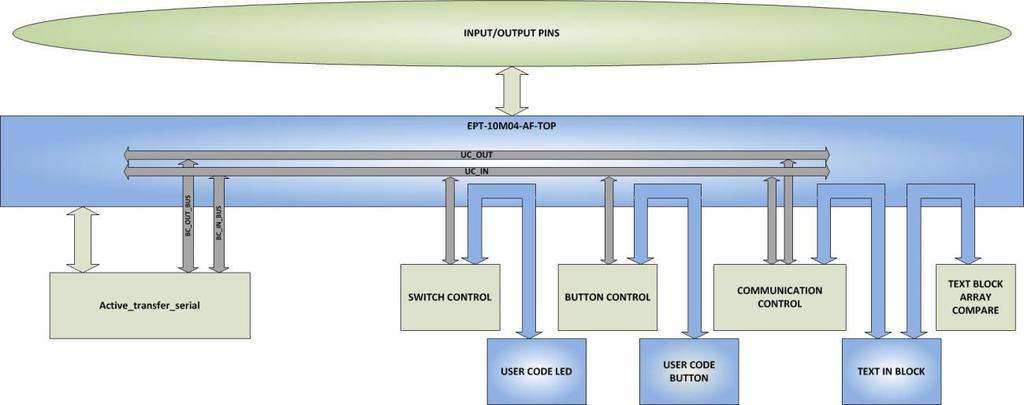
16 At the Browse window, double click on the output files folder. 16

17 Double click on the EPT_10M04_AF_Top.pof file. Click the Open button in the lower right corner. 17


18 Next, selet the checkbox under the Program/Configure of the Programmer Tool. 18
19 Click on the Start button to to start programming the FPGA. The Progress bar will indicate the progress of programming. When the programming is complete, the Progress bar will indicate success. 19

20 At this point, the MAXPROLOGIC is programmed and ready for use Using the Phone App Ensure the Joystick_v-1.0.apk is installed on your Android phone. Ensure the Odin-Link BLE Board is connected to the MaxProLogic J5 with both Pin 1 s aligned between the boards. Ensure the power is connected to the MaxProLogic. And, ensure the MAX10 is programmed with the EPT_10M04_AF_BLE_Driver project. Now, you are ready to use the app and observe the functioning of the project. Go to your Android apps and locate the JoyStick app. Click on the icon. The Joystick app will open and display on the screen. 20

21 Take note that there are four groups of functions on the JoyStick Android app: Switches have two states: on and off 21

22 buttons are single events Message block allows text message to and from the Odin-Link Ble board BLE Control buttons allow detection and connection to the Odin-Link BLE board Connecting the JoyStick app to the Odin-Link BLE Board 22
23 Ensure the MAX10 is programmed with the EPT_10M04_AF_BLE_Driver project and the power is applied to the MaxProLogic. When the power is applied to the MaxProLogic, all LEDs will blink twice. Next, you will pair the Android phone with the Odin-Link BLE Board. This is accomplished by pressing the Scan button first. **ADD PICTURE OF SCAN SCREEN WITH LOCATED DEVICES** Examine the text screen and verify that the app has located the Odin-Link BLE Board. **ADD PICTURE OF SCAN SCREEN WITH ODIN-LINK BOARD DISCOVERED** Press the Connect button. If the Android phone is within the BLE Advertising range of the Odin-Link, it will automatically connect. **ADD PICTURE OF SCAN SCREEN WITH MESSAGE DEVICE CONNECTED ** At this point the Android phone JoyStick app is connected with the Odin-Link BLE Board. Next, we will cover the operation of the functions Using the Switch Functions Using the Button Functions Using the Text Write/Receive Functions 2 The Active Transfer Serial Verilog Library The EPT_10M04_AF_BLE_Driver is a project that is designed to demonstrate the functionality of the Odin-Link BLE Board and the FPGA operation. There is a Verilog library called the Active_Transfer_serial. This library performs all of the serial decoding, storage, command decipher, and user interface control needed to receive commands from the Odin-Link BLE Board. 23

24 The user will include the Active_Transfer_Serial library in the project along with the user code. Compile and Synthesize the project using the Quartus Software Tool to produce a program file for download into the FPGA. 2.1 User Interface The Active_Serial_Transfer library has a relatively easy interface for user code. The interface is designed for flexibility and ease of use. It is written in Verilog and uses the 50MHz oscillator. It consists of four modules that access the user code. Active_Transfer_Serial.v Switch_Command.v Button_Command.v Communication_Command.v The user code will create a leaf instantiation to access the signals of each of these modules. 24
25 25
CPE 200L LABORATORY 4: INTRODUCTION TO DE2 BOARD UNIVERSITY OF NEVADA, LAS VEGAS GOALS: BACKGROUND:
 CPE 200L LABORATORY 4: INTRODUCTION TO DE2 BOARD DEPARTMENT OF ELECTRICAL AND COMPUTER ENGINEERING UNIVERSITY OF NEVADA, LAS VEGAS GOALS: Getting familiar with DE2 board installation, properties, usage.
MAXPROLOGIC FPGA DEVELOPMENT SYSTEM Data Sheet
 MAXPROLOGIC FPGA DEVELOPMENT SYSTEM Data Sheet The MaxProLogic is an FPGA development board that is designed to be user friendly and a great introduction into digital design for anyone. The MaxProLogic
Typical applications where a CPLD may be the best design approach:
 By: Carlos Barberis, dba Bartek Technologies Description of Bartek s CPLD1 development board. For some of us CPLD s are familiar devices and for others just another acronym in the electronic device industry.
EARTH PEOPLE TECHNOLOGY, Inc. MAXPROLOGIC DEVELOPMENT SYSTEM User Manual
 EARTH PEOPLE TECHNOLOGY, Inc MAXPROLOGIC DEVELOPMENT SYSTEM User Manual The MaxProLogic is an FPGA development board that is designed to be user friendly and a great introduction into digital design for
Configuration and programming minimodules MMfpga01 and MMfpga11
 MMfpga01 MMfpga11 Configuration and programming minimodules MMfpga01 and MMfpga11 1 Index 1. Instalation of the QUARTUS II Web Edition...3 2. How to install QUARTUS II Web Edition...5 3. Installation of
NOTE: This tutorial contains many large illustrations. Page breaks have been added to keep images on the same page as the step that they represent.
 CSE 352 Tutorial # 4 Synthesizing onto an FPGA Objectives This tutorial will walk you through the steps of implementing a design made in Active-HDL onto the Altera Cyclone II FPGA NOTE: This tutorial contains
EARTH PEOPLE TECHNOLOGY, Inc. MAXPROLOGIC DEVELOPMENT SYSTEM User Manual
 EARTH PEOPLE TECHNOLOGY, Inc MAXPROLOGIC DEVELOPMENT SYSTEM User Manual The MaxProLogic is an FPGA development board that is designed to be user friendly and a great introduction into digital design for
Laboratory Exercise 3 Comparative Analysis of Hardware and Emulation Forms of Signed 32-Bit Multiplication
 Laboratory Exercise 3 Comparative Analysis of Hardware and Emulation Forms of Signed 32-Bit Multiplication Introduction All processors offer some form of instructions to add, subtract, and manipulate data.
NIOS CPU Based Embedded Computer System on Programmable Chip
 1 Objectives NIOS CPU Based Embedded Computer System on Programmable Chip EE8205: Embedded Computer Systems This lab has been constructed to introduce the development of dedicated embedded system based
Altera EP4CE6 Mini Board. Hardware User's Guide
 Altera Hardware User's Guide 1. Introduction Thank you for choosing the! is a compact FPGA board which is designed based on device. It's a low-cost and easy-to-use platform for learning Altera's Cyclone
ULTIMATE CART FIRMWARE UPGRADE GUIDE
 Page 1 ULTIMATE CART FIRMWARE UPGRADE GUIDE This guide is intended as a reference to help understand the firmware upgrade process for the Ultimate Cart and highlight potential issues. It is not a comprehensive
Mechanical specifications Dimensions (L x W x H) 290 x 125 x mm Weight 445 g. Female DC Barrel Jack Socket 5.5x2.1 mm
 290 x 125 x mm Weight 445 g. Female DC Barrel Jack Socket 5.5x2.1 mm") Mirror Driver v1.0 The Mirror Driver v1.0 consists of two main hardware blocks. The first acts as a Data Acquisition (DAQ) board while the second is an FPGA evaluation kit which is used as a Digital Signal
Mirror Driver v1.0 The Mirror Driver v1.0 consists of two main hardware blocks. The first acts as a Data Acquisition (DAQ) board while the second is an FPGA evaluation kit which is used as a Digital Signal
1. Install Programmer Software
 Notes: Uses IST-12242-001A Programming Pod and 12-position 1 mm flat flex cable. If you encounter any problems while trying to program your unit, please contact Rebecca Afzal via email or call 419-536-5741
Tutorial for Altera DE1 and Quartus II
 Tutorial for Altera DE1 and Quartus II Qin-Zhong Ye December, 2013 This tutorial teaches you the basic steps to use Quartus II version 13.0 to program Altera s FPGA, Cyclone II EP2C20 on the Development
EARTH PEOPLE TECHNOLOGY, Inc. MegMax CPLD DEVELOPMENT SYSTEM User Manual
 EARTH PEOPLE TECHNOLOGY, Inc MegMax CPLD DEVELOPMENT SYSTEM User Manual The MegaMax CPLD development system provides an innovative method of developing and debugging programmable logic code. It also provides
CHAPTER 1 Introduction of the tnano Board CHAPTER 2 tnano Board Architecture CHAPTER 3 Using the tnano Board... 8
 CONTENTS CHAPTER 1 Introduction of the tnano Board... 2 1.1 Features...2 1.2 About the KIT...4 1.3 Getting Help...4 CHAPTER 2 tnano Board Architecture... 5 2.1 Layout and Components...5 2.2 Block Diagram
RedBoard Hookup Guide
 Page 1 of 11 RedBoard Hookup Guide CONTRIBUTORS: JIMB0 Introduction The Redboard is an Arduino-compatible development platform that enables quick-and-easy project prototyping. It can interact with real-world
Introduction to VHDL Design on Quartus II and DE2 Board
 ECP3116 Digital Computer Design Lab Experiment Duration: 3 hours Introduction to VHDL Design on Quartus II and DE2 Board Objective To learn how to create projects using Quartus II, design circuits and
Lab 2 EECE473 Computer Organization & Architecture University of Maine
 Lab 2: Verilog Programming Instructor: Yifeng Zhu 50 Points Objectives: 1. Quatus II Programming assignment: PIN assignments, LEDs, switches; 2. Download and test the design on Altera DE2 board 3. Create
FPGA RGB Matrix. Created by lady ada. Last updated on :15:42 PM UTC
 FPGA RGB Matrix Created by lady ada Last updated on 2017-12-27 09:15:42 PM UTC Guide Contents Guide Contents Overview Controlling the Adafruit 32x16 RGB LED Matrix with a DE0-Nano FPGA Board Prerequisites
Board Update Portal based on Nios II Processor with EPCQ (Arria 10 GX FPGA Development Kit)
") Board Update Portal based on Nios II Processor with EPCQ (Arria 10 GX FPGA Development Kit) Date: 1 December 2016 Revision:1.0 2015 Altera Corporation. All rights reserved. ALTERA, ARRIA, CYCLONE, HARDCOPY,
Board Update Portal based on Nios II Processor with EPCQ (Arria 10 GX FPGA Development Kit) Date: 1 December 2016 Revision:1.0 2015 Altera Corporation. All rights reserved. ALTERA, ARRIA, CYCLONE, HARDCOPY,
Freeduino USB 1.0. Arduino Compatible Development Board Starter Guide. 1. Overview
 Freeduino USB 1.0 Arduino Compatible Development Board Starter Guide 1. Overview 1 Arduino is an open source embedded development platform consisting of a simple development board based on Atmel s AVR
NIOS II Instantiating the Off-chip Trace Logic
 NIOS II Instantiating the Off-chip Trace Logic TRACE32 Online Help TRACE32 Directory TRACE32 Index TRACE32 Documents... ICD In-Circuit Debugger... Processor Architecture Manuals... NIOS... NIOS II Application
CPLD board datasheet EB
 CPLD board datasheet EB020-00-3 Contents. About this document... 2 2. General information... 3 3. Board layout... 4 4. Testing this product... 5 5. Circuit description... 6 Appendix Circuit diagram Copyright
DE2 Board & Quartus II Software
 January 23, 2015 Contact and Office Hours Teaching Assistant (TA) Sergio Contreras Office Office Hours Email SEB 3259 Tuesday & Thursday 12:30-2:00 PM Wednesday 1:30-3:30 PM contre47@nevada.unlv.edu Syllabus
How-To #7: Assemble an H-bridge Circuit Board
 How-To #7: Assemble an H-bridge Circuit Board Making a DC motor turn is relatively easy: simply connect the motor's terminals to a power supply. But what if the motor is to be controlled by an Arduino,
EMT1250 LABORATORY EXPERIMENT. EXPERIMENT # 7: VHDL and DE2 Board. Name: Date:
 EXPERIMENT # 7: VHDL and DE2 Board Name: Date: Equipment/Parts Needed: Quartus II R Web Edition V9.1 SP2 software by Altera Corporation USB drive to save your files Objective: Learn how to create and modify
ArduCAM CC3200 UNO board
 ArduCAM CC3200 UNO board User Guide Rev 1.2, Mar 2017 Table of Contents 1 Introduction... 2 2 Features... 3 3 Pin Definition... 4 4 Getting Started CC3200 with Energia... 5 4.1 Out of the Box Test... 5
Intel Galileo gen 2 Board
 Intel Galileo gen 2 Board The Arduino Intel Galileo board is a microcontroller board based on the Intel Quark SoC X1000, a 32- bit Intel Pentium -class system on a chip (SoC). It is the first board based
CSEE W4840 Embedded System Design Lab 1
 CSEE W4840 Embedded System Design Lab 1 Stephen A. Edwards Due January 31, 2008 Abstract Learn to use the Altera Quartus development envrionment and the DE2 boards by implementing a small hardware design
PCI-FPGA-1B User Guide
 PCI-FPGA-1B User Guide Rev 1.0 (Nov. 2012) Port City Instruments, LLC 8209 Market Street, Suite A271 Wilmington, NC 28411 (Tel) 866-456-2488 (Web) www.portcityinstruments.com Copyright 2012 Port City Instruments,
Manual of Board ET-PIC STAMP 18F8722-K22 ET-PIC STAMP 18F8722-K22
 ET-PIC STAMP 18F8722-K22 ET-PIC STAMP 18F8722-K22 is Board Microcontroller in a series of PIC18F87K22 80-Pin TQFP from Microchip. It designs I/O of MCU on board to interface with CONNECTOR in the format
ECE 3610 Microprocessing Systems Lab #1 Verilog Design of the TOC Using Quartus II
 ECE 3610 Microprocessing Systems Lab #1 Verilog Design of the TOC Using Quartus II This lab manual presents an introduction to the Quartus II Computer Aided Design (CAD) system. This manual gives step-by-step
Introduction to the Altera SOPC Builder Using Verilog Design
 Introduction to the Altera SOPC Builder Using Verilog Design This tutorial presents an introduction to Altera s SOPC Builder software, which is used to implement a system that uses the Nios II processor
FPGA Introductory Tutorial: Part 1
 FPGA Introductory Tutorial: Part 1 This tutorial is designed to assist in learning the basics of the Altera Quartus II v9.0 software. Part 1 of the tutorial will cover the basics of creating a Project,
EE 231 Fall Lab 1: Introduction to Verilog HDL and Altera IDE
 Lab 1: Introduction to Verilog HDL and Altera IDE Introduction In this lab you will design simple circuits by programming the Field-Programmable Gate Array (FPGA). At the end of the lab you should be able
Sidewinder Development Board rev 1.0
 33 Sidewinder Development Board rev 1.0 Features Altera MAX V CPLD 5M160ZT100C5 JTAG programmable USB programmable USB powered 12 On board LEDs 10 on board switches 3 RGB LEDs One 40 pin expansion headers
DOWNLOADING DESIGNS TO THE ALTERA DE10-LITE FPGA
 DOWNLOADING DESIGNS TO THE ALTERA DE10-LITE FPGA Consider the design of a three-bit prime number detector completed in the MSOE schematic entry tutorial. Figure 1 shows the block diagram and truth table.
ETVR360CAMW-User Guide
 ETVR360CAMW-User Guide TABLE OF CONTENTS 1. PARTS... 3 GETTING STARTED... 6 Charging the Battery... 6 Power On & Power Off... 6 Use Mode... 6 Independent Operation... 6 APP... 6 CONNECTING THROUGH WIFI...
Tutorial on Quartus II Introduction Using Verilog Code
 Tutorial on Quartus II Introduction Using Verilog Code (Version 15) 1 Introduction This tutorial presents an introduction to the Quartus II CAD system. It gives a general overview of a typical CAD flow
Quick Start Guide for the Turbo upsd DK3300-ELCD Development Kit- RIDE
 Contents: Circuit Board upsd DK3300-ELCD Development Board with a upsd3334d-40u6 MCU with Enhanced Graphic LCD RLINK-ST, a USB-based JTAG adapter from Raisonance for debugging with Raisonance Integrate
TI mmwave Training. mmwave Demo
 TI mmwave Training mmwave Contents Overview Requirements Software setup Pre-requisites Downloading the Lab Project Building the project Hardware setup Preparing the EVM Connecting the EVM Running the 2
EWAVE Inc Gracefield Ln. Dallas, Texas (972)
") EWAVE Inc. 7419 Gracefield Ln. Dallas, Texas 75248 (972) 248-2931 www.electrowave.com STAMPER User s Manual Version 1.0 Ewave Radio Modems covered in this manual: STAMPER INTRODUCTION... 3 1.1 FEATURES
EWAVE Inc. 7419 Gracefield Ln. Dallas, Texas 75248 (972) 248-2931 www.electrowave.com STAMPER User s Manual Version 1.0 Ewave Radio Modems covered in this manual: STAMPER INTRODUCTION... 3 1.1 FEATURES
NIOS CPU Based Embedded Computer System on Programmable Chip
 NIOS CPU Based Embedded Computer System on Programmable Chip EE8205: Embedded Computer Systems NIOS-II SoPC: PART-II 1 Introduction This lab has been constructed to introduce the development of dedicated
NIOS CPU Based Embedded Computer System on Programmable Chip
 NIOS CPU Based Embedded Computer System on Programmable Chip 1 Lab Objectives EE8205: Embedded Computer Systems NIOS-II SoPC: PART-I This lab has been constructed to introduce the development of dedicated
Use of ISP1507-AL Evaluation Boards
 Use of ISP1507-AL Evaluation Boards Application Note AN181103 Introduction Scope This document gives details on hardware and software for using and testing Insight SiP Bluetooth Low Energy module ISP1507-AL,
MINI-CAN User Manual. Issue 1.02
 MINI-CAN User Manual Issue 1.02 Kit Contents You should receive the following items in your MINI-CAN development kit: 1 - MINI-CAN Board 2 Programming Cable Figure 1 MINI-CAN Board Introduction Welcome
Chapter 2 Getting Hands on Altera Quartus II Software
 Chapter 2 Getting Hands on Altera Quartus II Software Contents 2.1 Installation of Software... 20 2.2 Setting Up of License... 21 2.3 Creation of First Embedded System Project... 22 2.4 Project Building
TOSR14x. TOSR14x USB/Wireless Relay Module. User Manual. Tinysine 2015 Version 1.2
 TOSR14x TOSR14x USB/Wireless Relay Module User Manual Tinysine Electronics @ 2015 Version 1.2 1 INTRODUCTION TOSR14x is an upgraded version of TOSR04. It supports password. It can be set to latching or
INTRODUCTION TO DE2 SYSTEM INTERFACES
 EECS:6660:0xxField Programmable Gate Arrays s08l5a.fm - 1 Lab Assignment #5 INTRODUCTION TO DE2 SYSTEM INTERFACES 1. OBJECTIVES - Becoming familiar with the system interface to seven segment LED displays
SAT0003_REV3.0 Test Procedure Texas Instruments for TPS40422 EVM Module
 Texas Instruments SAT0003_REV3.1 Test Procedure April 23, 2013 Scott McElroy Note: The SAT0003_REV3.1 is an evaluation module for the TPS40422 using the MSP430G2553 to test the functionality of the PMBus.
ZigBee USB Dongle ZSB series Data Sheet
 ZigBee USB Dongle ZSB series Data Sheet DS-ZSB Meshreen Content 1. Introduction... 3 1.1 Variants... 3 1.2 Key Features... 3 1.3 Applications... 3 2. Block Diagram... 4 3. Specification... 5 3.1 General
AN4782 Application note
 Application note Getting started with SPC56B-Discovery board Introduction The SPC560B-Discovery board, hereafter described as SPC560B-DIS, is an evaluation tool supporting STMicroelectronics SPC56B-Line
Tutorial on Quartus II Introduction Using Schematic Designs
 Tutorial on Quartus II Introduction Using Schematic Designs (Version 15) 1 Introduction This tutorial presents an introduction to the Quartus II CAD system. It gives a general overview of a typical CAD
TI mmwave Training. xwr16xx mmwave Demo
 TI mmwave Training xwr16xx mmwave Contents Overview Requirements Software setup Pre-requisites Downloading the Lab Project Building the project Hardware setup Preparing the EVM Connecting the EVM Running
The University of Toledo EECS:6660:0xxField Programmable Gate Arrays s09l1.fm - 1 Dr. A.D. Johnson
 EECS:6660:0xxField Programmable Gate Arrays s09l1.fm - 1 Lab Assignment #1 Due: Friday, February 27 2009 Introduction to Altera Quartus II Environment using VHDL Entry 1. Objectives - introduction to Quartus
Arduino Micro Breadboard Laboratory Interface Processor (Micro BLIP) User Manual
 User Manual") Arduino Micro Breadboard Laboratory Interface Processor (Micro BLIP) MicroBLIP circuit board v2.0 Operating System v2.0.0 1/22/2019 User Manual 2 1 Setup and Operation 1.1 Introduction For the past ten
Arduino Micro Breadboard Laboratory Interface Processor (Micro BLIP) MicroBLIP circuit board v2.0 Operating System v2.0.0 1/22/2019 User Manual 2 1 Setup and Operation 1.1 Introduction For the past ten
Wireless Digital Photo Frame Quick Start Guide
 Wireless Digital Photo Frame Quick Start Guide MODEL: AD1021W Package Contents Wireless Digital Photo Frame Quick Start Guide Power Adaptor Stand Limited Warranty Instructions Power on/off Speaker SD/SDHC
University of Massachusetts Amherst Computer Systems Lab 2 (ECE 354) Spring Lab 1: Using Nios 2 processor for code execution on FPGA
 Spring Lab 1: Using Nios 2 processor for code execution on FPGA") University of Massachusetts Amherst Computer Systems Lab 2 (ECE 354) Spring 2007 Lab 1: Using Nios 2 processor for code execution on FPGA Objectives: After the completion of this lab: 1. You will understand
University of Massachusetts Amherst Computer Systems Lab 2 (ECE 354) Spring 2007 Lab 1: Using Nios 2 processor for code execution on FPGA Objectives: After the completion of this lab: 1. You will understand
PCI-FRM11. User s Manual. PCI-FRM11 User s Manual (Rev 1.1)
") PCI-FRM11 User s Manual Windows, Windows2000, Windows NT and Windows XP are trademarks of Microsoft. We acknowledge that the trademarks or service names of all other organizations mentioned in this document
PCI-FRM11 User s Manual Windows, Windows2000, Windows NT and Windows XP are trademarks of Microsoft. We acknowledge that the trademarks or service names of all other organizations mentioned in this document
Getting Started with STK200 Dragon
 Getting Started with STK200 Dragon Introduction This guide is designed to get you up and running with main software and hardware. As you work through it, there could be lots of details you do not understand,
M32 Development Board
 M32 Development Board User Guide Document Control Information This Document Release Date: 12th March 2006 This Document Version: 1.0 Document History Author Release Date Reference Release Notes JSL 23rd
LAVASynC+ Installation Manual
 LAVASynC+ Installation Manual October 10, 2018 Revision A04 Abstract The LAVASynC family of products permits the charging of select Samsung tablets and mobile phones while simultaneously interacting with
User s Guide IoT Microcontroller Development Kit
 User s Guide IoT Microcontroller Development Kit 1.0 Introduction 2 1.1 Features 2 1.2 Board Pictures 3 2.0 Hardware 4 2.1 Bill of Materials 4 2.2 Pin Map Diagram 5 2.3 Block Diagram 6 2.4 Board Revisions
Introduction to the Altera SOPC Builder Using Verilog Designs. 1 Introduction
 Introduction to the Altera SOPC Builder Using Verilog Designs 1 Introduction This tutorial presents an introduction to Altera s SOPC Builder software, which is used to implement a system that uses the
Use of ISP1807-LR Evaluation Boards
 Use of ISP1807-LR Evaluation Boards Application Note AN181104 Introduction Scope This document gives details on hardware and software for using and testing Insight SiP Bluetooth Low Energy module ISP1807-LR,
Arduino Dock 2. The Hardware
 Arduino Dock 2 The Arduino Dock 2 is our supercharged version of an Arduino Uno R3 board. These two boards share the same microcontroller, the ATmel ATmega328P microcontroller (MCU), and have identical
EE 231 Fall EE 231 Lab 2
 EE 231 Lab 2 Introduction to Verilog HDL and Quartus In the previous lab you designed simple circuits using discrete chips. In this lab you will do the same but by programming the CPLD. At the end of the
CSE P567 - Winter 2010 Lab 1 Introduction to FGPA CAD Tools
 CSE P567 - Winter 2010 Lab 1 Introduction to FGPA CAD Tools This is a tutorial introduction to the process of designing circuits using a set of modern design tools. While the tools we will be using (Altera
Quick Start Guide: YROTATE-IT-S5D9
 Document Contents 1.0 Introduction 1 2.0 Board Layout 1 3.0 Initial Board Configuration 2 4.0 PC Graphical User Interface (GUI) Software Installation 3 5.0 Installing USB Drivers 4 6.0 Using the Graphical
HOW TO USE ESP8266 WITH ARDUINO IDE
 HOW TO USE ESP8266 WITH ARDUINO IDE This document applies for the following products: ESP8266-EVB; ESP8266-EVB-BAT; ESP8266-EVB-BAT-BOX Document revision B, February 2017 All boards produced by Olimex
E85: Digital Design and Computer Engineering Lab 2: FPGA Tools and Combinatorial Logic Design
 E85: Digital Design and Computer Engineering Lab 2: FPGA Tools and Combinatorial Logic Design Objective The purpose of this lab is to learn to use Field Programmable Gate Array (FPGA) tools to simulate
475 Electronics for physicists Introduction to FPGA programming
 475 Electronics for physicists Introduction to FPGA programming Andrej Seljak, Gary Varner Department of Physics University of Hawaii at Manoa November 18, 2015 Abstract Digital circuits based on binary
Experiment 18 Full Adder and Parallel Binary Adder
 Objectives Experiment 18 Full Adder and Parallel Binary Adder Upon completion of this laboratory exercise, you should be able to: Create and simulate a full adder in VHDL, assign pins to the design, and
TKT-2431 SoC design. Introduction to exercises. SoC design / September 10
 TKT-2431 SoC design Introduction to exercises Assistants: Exercises and the project work Juha Arvio juha.arvio@tut.fi, Otto Esko otto.esko@tut.fi In the project work, a simplified H.263 video encoder is
Laboratory Exercise 8
 Laboratory Exercise 8 Memory Blocks In computer systems it is necessary to provide a substantial amount of memory. If a system is implemented using FPGA technology it is possible to provide some amount
MAXREFDES43# ZedBoard Quick Start Guide
 MAXREFDES43# ZedBoard Quick Start Guide Rev 0; 4/15 Maxim Integrated cannot assume responsibility for use of any circuitry other than circuitry entirely embodied in a Maxim Integrated product. No circuit
Chapter 2: Hardware Design Flow Using Verilog in Quartus II
 Chapter 2: Hardware Design Flow Using Verilog in Quartus II 2.1 Introduction to Quartus II System Development Software This chapter is an introduction to the Quartus II software that will be used for analysis
HOW TO UPGRADE ESP8266 BOARDS USING ESP FLASH DOWNLOAD TOOLS
 HOW TO UPGRADE ESP8266 BOARDS USING ESP FLASH DOWNLOAD TOOLS This document applies for the following products: ESP8266-EVB; ESP8266-EVB-BAT; ESP8266-EVB-BAT-BOX; MOD-ESP8266-WIFI-DEV; MOD-ESP8266-WIFI;
LPC2468 Industrial Reference Design Platform System Development Kit Version 1.2. August 2008
 QuickStart Guide LPC2468 Industrial Reference Design Platform System Development Kit Version 1.2 August 2008 1.0 System Overview The LPC2468 Industrial Reference Design (IRD) is a platform targeted at
ARROW ARIS EDGE Board User s Guide 27/09/2017
 ARROW ARIS EDGE Board User s Guide All information contained in these materials, including products and product specifications, represents information on the product at the time of publication and is subject
Laboratory Exercise 1
 Laboratory Exercise 1 Switches, Lights, and Multiplexers The purpose of this exercise is to learn how to connect simple input and output devices to an FPGA chip and implement a circuit that uses these
UnoMax CPLD Development System. Data Sheet
 UnoMax CPLD Development System Data Sheet The UnoMax is a small form factor CPLD Development System. The core functions of the UnoMax are a two channel USB to Serial chip, 570 Logic Cell CPLD and a four
This manual provides information for the final user application developer on how to use SPC57S-Discovery microcontroller evaluation board.
 User manual SPC570S-DISP: Discovery+ Evaluation Board Introduction This manual provides information for the final user application developer on how to use SPC57S-Discovery microcontroller evaluation board.
Mechanical Assembly Guide
 Mechanical Assembly Guide Intel Aero Platform for UAVs October 06 Table of Contents Contents of Compute Board Compute Board Features Contents of Vision Accessory Kit (Optional) Contents of Enclosure Kit
WAVETEK BLE-WT51822AA/AB. Revision History. Bluetooth low energy Module WT51822AA (256k) /AB (128k) (Bluetooth Low Energy BT4.0) PRODUCT SPECIFICATION
 /AB (128k) (Bluetooth Low Energy BT4.0) PRODUCT SPECIFICATION") Bluetooth low energy Module WT51822AA (256k) /AB (128k) (Bluetooth Low Energy BT4.0) PRODUCT SPECIFICATION Part number: BLE WT51822AA/AB Wavetek has developed a module which supports Bluetooth Low Energy
Bluetooth low energy Module WT51822AA (256k) /AB (128k) (Bluetooth Low Energy BT4.0) PRODUCT SPECIFICATION Part number: BLE WT51822AA/AB Wavetek has developed a module which supports Bluetooth Low Energy
AVR Intermediate Development Board. Product Manual. Contents. 1) Overview 2) Features 3) Using the board 4) Troubleshooting and getting help
 Overview 2) Features 3) Using the board 4) Troubleshooting and getting help") AVR Intermediate Development Board Product Manual Contents 1) Overview 2) Features 3) Using the board 4) Troubleshooting and getting help 1. Overview 2. Features The board is built on a high quality FR-4(1.6
AVR Intermediate Development Board Product Manual Contents 1) Overview 2) Features 3) Using the board 4) Troubleshooting and getting help 1. Overview 2. Features The board is built on a high quality FR-4(1.6
UF-3701 Power Board Construction Guide
 Page 1/5 Soldering and Part Placement See the Chapter 3 of the MIT 6270 Manual for information on electronic assembly, including soldering techniques and component mounting. Construction Information All
Lab 2: Introduction to Verilog HDL and Quartus
 Lab 2: Introduction to Verilog HDL and Quartus September 16, 2008 In the previous lab you designed simple circuits using discrete chips. In this lab you will do the same but by programming the CPLD. At
NFC NUTSHELL KIT. MCU Modules USER MANUAL REVISION GMMC GmbH Keywords Abstract. Document information
 USER MANUAL REVISION 1.23 Document information Info Keywords Abstract Content User Manual GMMC This document describes how to use of the GMMC s NFC Nutshell KIT and its related tools GMMC GmbH www.gmmc-biz.com
Getting Started Guide RS-EDP & XC167 CPU Module. Version 2 10th June 2010
 Getting Started Guide RS-EDP & XC167 CPU Module Version 2 10th June 2010 Electrocomponents plc Page 1 Contents 1. Introduction 3 2. Development Tool Support 4 2.1 FTDI Based USB to JTAG Converter... 4
3D Magnetic Sensor 2 Go - TLE493D-A2B6
 TLE493D-A2B6 3D-MS2GO User Manual About this document Scope and purpose This document provides an introduction to the 3D Magnetic Sensor 2 Go kit and should enable the reader to efficiently carry out own
QUICK START GUIDE TO THE JUMPSTART MICROBOX
 QUICK START GUIDE TO THE JUMPSTART MICROBOX JumpStart MicroBox Contents The JumpStart MicroBox has three hardware components: Nucleo board from ST. This board contains the Cortex M0 STM32F030 microcontroller
PRELAB! Read the entire lab, and complete the prelab questions (Q1- Q3) on the answer sheet before coming to the laboratory.
 on the answer sheet before coming to the laboratory.") PRELAB! Read the entire lab, and complete the prelab questions (Q1- Q3) on the answer sheet before coming to the laboratory. 1.0 Objectives In this lab you will get familiar with the concept of using the
PRELAB! Read the entire lab, and complete the prelab questions (Q1- Q3) on the answer sheet before coming to the laboratory. 1.0 Objectives In this lab you will get familiar with the concept of using the
SR-201 Network Relay Quick Start Guide
 SR-201 Network Relay Quick Start Guide Table of Content Connect to your device...2 Change configurations...3 Setup remote control via internet...4 Android software...5 Integrate to your applications...6
8051 Intermidiate Development Board. Product Manual. Contents. 1) Overview 2) Features 3) Using the board 4) Troubleshooting and getting help
 Overview 2) Features 3) Using the board 4) Troubleshooting and getting help") 8051 Intermidiate Development Board Product Manual Contents 1) Overview 2) Features 3) Using the board 4) Troubleshooting and getting help 1. Overview 2. Features The board is built on a high quality FR-4(1.6
8051 Intermidiate Development Board Product Manual Contents 1) Overview 2) Features 3) Using the board 4) Troubleshooting and getting help 1. Overview 2. Features The board is built on a high quality FR-4(1.6
2 nd Year Laboratory. Experiment: FPGA Design with Verilog. Department of Electrical & Electronic Engineering. Imperial College London.
 Department of Electrical & Electronic Engineering 2 nd Year Laboratory Experiment: FPGA Design with Verilog Objectives By the end of this experiment, you should know: How to design digital circuits using
ECE 353 Lab 4. MIDI Receiver in Verilog. Professor Daniel Holcomb UMass Amherst Fall 2016
 ECE 353 Lab 4 MIDI Receiver in Verilog Professor Daniel Holcomb UMass Amherst Fall 2016 Timeline and Grading for Lab 4 Lectures on 11/15 and 11/17 Due on 12/12 Demos in Duda hall Schedule will be posted
P&E Microcomputer Systems, Inc. P.O. Box 2044, Woburn, MA 01888, USA
 P&E Microcomputer Systems, Inc. P.O. Box 2044, Woburn, MA 01888, USA TEL: (617) 353-9206 FAX: (617) 353-9205 http://www.pemicro.com USB-ML-MON08 Rev D Technical Summary Document # PE3357, Version 1.01
3. The circuit is composed of 1 set of Relay circuit.
 Part Number : Product Name : FK-FA1420 ONE CHANNEL 12V RELAY MODULE This is the experimental module for a relay controller as the fundamental controlling programming. It is adaptable or is able to upgrade