Philadelphia University Department of Computer Science. By Dareen Hamoudeh
|
|
|
- Jessie Powell
- 5 years ago
- Views:
Transcription

1 Philadelphia University Department of Computer Science By Dareen Hamoudeh
2 1.REGISTERS
3 WHAT IS REGISTER? register is a quickly accessible location available to a computer's central processing unit (CPU). Register are used to quickly accept, store, and transfer data and instructions that are being used immediately by the CPU. Almost all computers, load data from a larger memory into registers where it is used for arithmetic operations and is manipulated or tested by machine instructions. Manipulated data is then often stored back to main memory. Processor registers are normally at the top of the memory hierarchy, and provide the fastest way to access data. A register may hold an instruction, a storage address, or any kind of data (such as a bit sequence or individual characters).
4

5 WHERE IS THE LOCATION OF REGISTERS
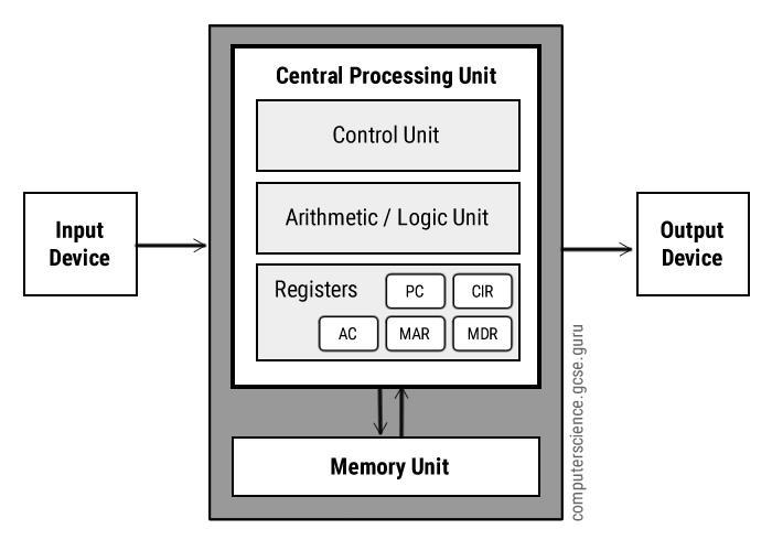
6
7 TYPES OF REGISTERS There are various types of Registers those are used for various purpose. Among of the some Mostly used Registers named as MAR: Memory Address Register AC : Accumulator. DR: Data Register. AR: Address Register. PC: Program counter. MDR: Memory Data Register. Index register Memory Buffer Register.

8 TYPES OF REGISTERS
9 VIDEOS How CPU works: Inside the CPU: Inside Microchip:
10 REGISTER CONSTRUCTION. Registers are normally measured by the number of bits they can hold, for example, an 8-bit register or a 32- bit register. A register is simply is: a collection of edge triggered flip-flops( each is capable to store one bit only). May have combinational gates that perform certain tasks. So, flip-flops hold the binary information, and gates control how/when new information transferred to the register. 4- bit register
11 4 BIT REGISTER 4 D flip-flops. 4 inputs. Clock input. Clear input. Outputs. How does it work: Clock triggers the flip-flops at the rising edge of pulses. Binary data on the inputs transferred to the flip-flops. The outputs sampled to obtain the information stored in the register. Clear input if zero all flip-flops are reset. Loading is transferring new information to the register.
12 REGISTER WITH PARALLEL LOAD digital systems have a master clock generator that supplies a continuous train of clock pulses. pulses are applied to all flip-flops and registers in the system. If all the bits of the register are loaded simultaneously with a common clock pulse. we say that the loading is done in parallel. A separate control signal must be used to decide which register operation will execute at each clock pulse. Can we use gates on the clock inputs??
13 REGISTER WITH PARALLEL LOAD inserting gates into the clock path means that logic is performed with clock pulses. The insertion of logic gates produces uneven propagation delays between the master clock and the inputs of flip-flops. To fully synchronize the system: all clock pulses must arrive at the same time anywhere in the system. Solution: to control the operation of the register with the D inputs. rather than controlling the clock in the C inputs of the flip-flops. This creates the effect of a gated clock. but without affecting the clock path of the circuit.
14 The additional gates implement a two channel mux whose output drives the input to the register with either the data bus or the output of the register. The load input to the register determines the action to be taken with each clock pulse. Load =1 data at the four external inputs are transferred into the register with the next positive edge of the clock (Loading). Load=0 outputs of the flip-flops are connected to their respective inputs (Hold).
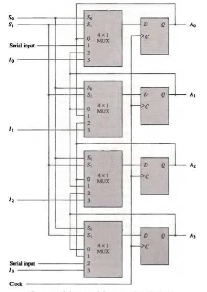
15 SHIFT REGISTER Flip Flops connected in a way that the output of one flip flop could serve as the input of the other flip-flop, depending on the type of shift registers being created. Shift registers are basically a type of register which have the ability to transfer ( shift ) data in one or both directions.
16
17 BIDIRECTIONAL REGISTER WITH PARALLEL LOAD (UNIVERSAL SHIFT REGISTER) Construction:
18 UNIVERSAL SHIFT REGISTER FUNCTION TABLE
19

20 SHIFT REGISTER Toshiba TC4015BP - Dual 4-Stage Static Shift Register (with serial input/parallel output)
21 MEMORY UNIT A memory unit is a device to which binary information is transferred for storage and from which information is retrieved when needed for processing. When data processing takes place, information from memory is transferred to selected registers in the processing unit. Intermediate and final results obtained in the processing unit are transferred back to be stored in memory. A memory unit is a collection of cells capable of storing a large quantity of binary information.
22 MEMORY UNIT Memory stores binary information in groups of bits called Words. Memory Word is group of 1 s and 0 s and may represent instruction code, one or more alphanumeric character Byte is group of 8 bits. Number of bits in a word, is multiple of 8: 16-bit word contains 2 bytes. 32-bit word contains 4 bytes. Structure of memory is specified by the number of words and the number of bits in each word. Each word in memory is assigned an identification number called an address
23 MEMORY ADDRESS Addresses start from 0 up 2 k - I. where k is the number of address lines. Memories vary greatly in size: 1024 words = 1024 bytes= 1kilobyte needs 10 address lines (2 10 ). M = 2 20 needs 20 address lines. G = 2 30 needs 30 address lines. 64K= 2 16 (64=2 6 + k=2 10 ) 4G= 2 32

24 EXAMPLE (1K X 16 memory) has: 10 bits in the address (k=2 10 ) and 16 bits in each word. A word in memory is selected by its binary address. When a word is read or written, the memory operates on all 16 bits as a single unit.
25 SOLVE THIS 64K X 10 memory???
26 TYPES OF MEMORIES RAM : Random Access Memory Construction: Data input Lines Data output lines, Address selection lines, Control lines that specify the direction of transfer Operations: Write read
27 RAM OPERATIONS Steps of transferring a new word to be stored into memory (Write): 1. Apply the binary address of the desired word to the address lines. 2. Apply the data bits that must be stored in memory to the data input lines. 3. Activate the write input. Steps of transferring a stored word out of memory (Read): 1. Apply the binary address of the desired word to the address lines. 2. Activate the read input.
28 TYPES OF MEMORIES ROM: Read Only Memory m x n ROM: m: number of words. n: number of bits per word.

29
Computer Architecture: Part III. First Semester 2013 Department of Computer Science Faculty of Science Chiang Mai University
 Computer Architecture: Part III First Semester 2013 Department of Computer Science Faculty of Science Chiang Mai University Outline Decoders Multiplexers Registers Shift Registers Binary Counters Memory
REGISTER TRANSFER LANGUAGE
 REGISTER TRANSFER LANGUAGE The operations executed on the data stored in the registers are called micro operations. Classifications of micro operations Register transfer micro operations Arithmetic micro
COMPUTER ARCHITECTURE AND ORGANIZATION Register Transfer and Micro-operations 1. Introduction A digital system is an interconnection of digital
 Register Transfer and Micro-operations 1. Introduction A digital system is an interconnection of digital hardware modules that accomplish a specific information-processing task. Digital systems vary in
Computer Architecture
 Computer Architecture Lecture 1: Digital logic circuits The digital computer is a digital system that performs various computational tasks. Digital computers use the binary number system, which has two
Register Transfer and Micro-operations
 Register Transfer Language Register Transfer Bus Memory Transfer Micro-operations Some Application of Logic Micro Operations Register Transfer and Micro-operations Learning Objectives After reading this
Computer Systems Organization
 The IAS (von Neumann) Machine Computer Systems Organization Input Output Equipment Stored Program concept Main memory storing programs and data ALU operating on binary data Control unit interpreting instructions
Computer Organization
 A Text Book of Computer Organization and Architecture Prof. JATINDER SINGH Director, GGI, Dhaliwal Er. AMARDEEP SINGH M.Tech (IT) AP&HOD, Deptt.of CSE, SVIET, Banur Er. GURJEET SINGH M.Tech (CSE) Head,
UNIT - V MEMORY P.VIDYA SAGAR ( ASSOCIATE PROFESSOR) Department of Electronics and Communication Engineering, VBIT
 Department of Electronics and Communication Engineering, VBIT") UNIT - V MEMORY P.VIDYA SAGAR ( ASSOCIATE PROFESSOR) contents Memory: Introduction, Random-Access memory, Memory decoding, ROM, Programmable Logic Array, Programmable Array Logic, Sequential programmable
UNIT - V MEMORY P.VIDYA SAGAR ( ASSOCIATE PROFESSOR) contents Memory: Introduction, Random-Access memory, Memory decoding, ROM, Programmable Logic Array, Programmable Array Logic, Sequential programmable
Microprocessors/Microcontrollers
 Microprocessors/Microcontrollers A central processing unit (CPU) fabricated on one or more chips, containing the basic arithmetic, logic, and control elements of a computer that are required for processing
Memory System Design. Outline
 Memory System Design Chapter 16 S. Dandamudi Outline Introduction A simple memory block Memory design with D flip flops Problems with the design Techniques to connect to a bus Using multiplexers Using
1 MALP ( ) Unit-1. (1) Draw and explain the internal architecture of 8085.
 Unit-1. (1) Draw and explain the internal architecture of 8085.") (1) Draw and explain the internal architecture of 8085. The architecture of 8085 Microprocessor is shown in figure given below. The internal architecture of 8085 includes following section ALU-Arithmetic
(1) Draw and explain the internal architecture of 8085. The architecture of 8085 Microprocessor is shown in figure given below. The internal architecture of 8085 includes following section ALU-Arithmetic
STRUCTURE OF DESKTOP COMPUTERS
 Page no: 1 UNIT 1 STRUCTURE OF DESKTOP COMPUTERS The desktop computers are the computers which are usually found on a home or office desk. They consist of processing unit, storage unit, visual display
University of Technology
 University of Technology Lecturer: Dr. Sinan Majid Course Title: microprocessors 4 th year Lecture 13 Counters Overview Counters are important components in computers The increment or decrement by one
Computer Organization
 INF 101 Fundamental Information Technology Computer Organization Assistant Prof. Dr. Turgay ĐBRĐKÇĐ Course slides are adapted from slides provided by Addison-Wesley Computing Fundamentals of Information
Combinational and sequential circuits (learned in Chapters 1 and 2) can be used to create simple digital systems.
 can be used to create simple digital systems.") REGISTER TRANSFER AND MICROOPERATIONS Register Transfer Language Register Transfer Bus and Memory Transfers Arithmetic Microoperations Logic Microoperations Shift Microoperations Arithmetic Logic Shift
REGISTER TRANSFER AND MICROOPERATIONS Register Transfer Language Register Transfer Bus and Memory Transfers Arithmetic Microoperations Logic Microoperations Shift Microoperations Arithmetic Logic Shift
CHAPTER 4: Register Transfer Language and Microoperations
 CS 224: Computer Organization S.KHABET CHAPTER 4: Register Transfer Language and Microoperations Outline Register Transfer Language Register Transfer Bus and Memory Transfers Arithmetic Microoperations
Chapter 5. Computer Architecture Organization and Design. Computer System Architecture Database Lab, SANGJI University
 Chapter 5. Computer Architecture Organization and Design Computer System Architecture Database Lab, SANGJI University Computer Architecture Organization and Design Instruction Codes Computer Registers
Microcomputer Architecture and Programming
 IUST-EE (Chapter 1) Microcomputer Architecture and Programming 1 Outline Basic Blocks of Microcomputer Typical Microcomputer Architecture The Single-Chip Microprocessor Microprocessor vs. Microcontroller
machine cycle, the CPU: (a) Fetches an instruction, (b) Decodes the instruction, (c) Executes the instruction, and (d) Stores the result.
 Fetches an instruction, (b) Decodes the instruction, (c) Executes the instruction, and (d) Stores the result.") Central Processing Unit (CPU) A processor is also called the CPU, and it works hand in hand with other circuits known as main memory to carry out processing. The CPU is the "brain" of the computer; it
Central Processing Unit (CPU) A processor is also called the CPU, and it works hand in hand with other circuits known as main memory to carry out processing. The CPU is the "brain" of the computer; it
 Part A Questions 1. What is an ISP? ISP stands for Instruction Set Processor. This unit is simply called as processor which executes machine instruction and coordinates the activities of other units..
REGISTER TRANSFER AND MICROOPERATIONS
 1 REGISTER TRANSFER AND MICROOPERATIONS Register Transfer Language Register Transfer Bus and Memory Transfers Arithmetic Microoperations Logic Microoperations Shift Microoperations Arithmetic Logic Shift
Scheme G. Sample Test Paper-I
 Sample Test Paper-I Marks : 25 Times:1 Hour 1. All questions are compulsory. 2. Illustrate your answers with neat sketches wherever necessary. 3. Figures to the right indicate full marks. 4. Assume suitable
REGISTER TRANSFER AND MICROOPERATIONS
 REGISTER TRANSFER AND MICROOPERATIONS Register Transfer Language Register Transfer Bus and Memory Transfers Arithmetic Microoperations Logic Microoperations Shift Microoperations Arithmetic Logic Shift
CHAPTER SIX BASIC COMPUTER ORGANIZATION AND DESIGN
 CHAPTER SIX BASIC COMPUTER ORGANIZATION AND DESIGN 6.1. Instruction Codes The organization of a digital computer defined by: 1. The set of registers it contains and their function. 2. The set of instructions
For Example: P: LOAD 5 R0. The command given here is used to load a data 5 to the register R0.
 Register Transfer Language Computers are the electronic devices which have several sets of digital hardware which are inter connected to exchange data. Digital hardware comprises of VLSI Chips which are
Reference Sheet for C112 Hardware
 Reference Sheet for C112 Hardware 1 Boolean Algebra, Gates and Circuits Autumn 2016 Basic Operators Precedence : (strongest),, + (weakest). AND A B R 0 0 0 0 1 0 1 0 0 1 1 1 OR + A B R 0 0 0 0 1 1 1 0
Unit II Basic Computer Organization
 1. Define the term. Internal Organization-The internal organization of a digital system is defined by the sequence of microoperations it performs on data stored in its registers. Program- A program is
Altera FLEX 8000 Block Diagram
 Altera FLEX 8000 Block Diagram Figure from Altera technical literature FLEX 8000 chip contains 26 162 LABs Each LAB contains 8 Logic Elements (LEs), so a chip contains 208 1296 LEs, totaling 2,500 16,000
Code No: R Set No. 1
 Code No: R059210504 Set No. 1 II B.Tech I Semester Supplementary Examinations, February 2007 DIGITAL LOGIC DESIGN ( Common to Computer Science & Engineering, Information Technology and Computer Science
(Advanced) Computer Organization & Architechture. Prof. Dr. Hasan Hüseyin BALIK (5 th Week)
 Computer Organization & Architechture. Prof. Dr. Hasan Hüseyin BALIK (5 th Week)") + (Advanced) Computer Organization & Architechture Prof. Dr. Hasan Hüseyin BALIK (5 th Week) + Outline 2. The computer system 2.1 A Top-Level View of Computer Function and Interconnection 2.2 Cache Memory
+ (Advanced) Computer Organization & Architechture Prof. Dr. Hasan Hüseyin BALIK (5 th Week) + Outline 2. The computer system 2.1 A Top-Level View of Computer Function and Interconnection 2.2 Cache Memory
COMPUTER ORGANIZATION AND ARCHITECTURE
 Page 1 1. Which register store the address of next instruction to be executed? A) PC B) AC C) SP D) NONE 2. How many bits are required to address the 128 words of memory? A) 7 B) 8 C) 9 D) NONE 3. is the
Computer architecture Assignment 3
 Computer architecture Assignment 3 1- An instruction at address 14E in the basic computer has I=0, an operation code of the AND instruction, and an address part equal to 109(all numbers are in hexadecimal).
UNIT-III REGISTER TRANSFER LANGUAGE AND DESIGN OF CONTROL UNIT
 UNIT-III 1 KNREDDY UNIT-III REGISTER TRANSFER LANGUAGE AND DESIGN OF CONTROL UNIT Register Transfer: Register Transfer Language Register Transfer Bus and Memory Transfers Arithmetic Micro operations Logic
Computer Architecture Programming the Basic Computer
 4. The Execution of the EXCHANGE Instruction The EXCHANGE routine reads the operand from the effective address and places it in DR. The contents of DR and AC are interchanged in the third microinstruction.
Levels in Processor Design
 Levels in Processor Design Circuit design Keywords: transistors, wires etc.results in gates, flip-flops etc. Logical design Putting gates (AND, NAND, ) and flip-flops together to build basic blocks such
Basic Processing Unit: Some Fundamental Concepts, Execution of a. Complete Instruction, Multiple Bus Organization, Hard-wired Control,
 UNIT - 7 Basic Processing Unit: Some Fundamental Concepts, Execution of a Complete Instruction, Multiple Bus Organization, Hard-wired Control, Microprogrammed Control Page 178 UNIT - 7 BASIC PROCESSING
The Itanium Bit Microprocessor Report
 The Itanium - 1986 8 Bit Microprocessor Report By PRIYANK JAIN (02010123) Group # 11 Under guidance of Dr. J. K. Deka & Dr. S. B. Nair Department of Computer Science & Engineering Indian Institute of Technology,
MICROPROCESSOR MICROPROCESSOR. From the above description, we can draw the following block diagram to represent a microprocessor based system: Output
 8085 SATISH CHANDRA What is a Microprocessor? The word comes from the combination micro and processor. Processor means a device that processes whatever. In this context, processor means a device that processes
5-1 Instruction Codes
 Chapter 5: Lo ai Tawalbeh Basic Computer Organization and Design 5-1 Instruction Codes The Internal organization of a digital system is defined by the sequence of microoperations it performs on data stored
Blog -
 . Instruction Codes Every different processor type has its own design (different registers, buses, microoperations, machine instructions, etc) Modern processor is a very complex device It contains Many
csitnepal Unit 3 Basic Computer Organization and Design
 Unit 3 Basic Computer Organization and Design Introduction We introduce here a basic computer whose operation can be specified by the resister transfer statements. Internal organization of the computer
CHAPTER 5 : Introduction to Intel 8085 Microprocessor Hardware BENG 2223 MICROPROCESSOR TECHNOLOGY
 CHAPTER 5 : Introduction to Intel 8085 Hardware BENG 2223 MICROPROCESSOR TECHNOLOGY The 8085A(commonly known as the 8085) : Was first introduced in March 1976 is an 8-bit microprocessor with 16-bit address
Ripple Counters. Lecture 30 1
 Ripple Counters A register that goes through a prescribed sequence of states upon the application of input pulses is called a counter. The input pulses may be clock pulses, or they may originate from some
Code No: R Set No. 1
 Code No: R059210504 Set No. 1 II B.Tech I Semester Regular Examinations, November 2006 DIGITAL LOGIC DESIGN ( Common to Computer Science & Engineering, Information Technology and Computer Science & Systems
Lecture 13: Memory and Programmable Logic
 Lecture 13: Memory and Programmable Logic Syed M. Mahmud, Ph.D ECE Department Wayne State University Aby K George, ECE Department, Wayne State University Contents Introduction Random Access Memory Memory
Department of Computer Science and Engineering CS6303-COMPUTER ARCHITECTURE UNIT-I OVERVIEW AND INSTRUCTIONS PART A
 Department of Computer Science and Engineering CS6303-COMPUTER ARCHITECTURE UNIT-I OVERVIEW AND INSTRUCTIONS PART A 1.Define Computer Architecture Computer Architecture Is Defined As The Functional Operation
Architecture of 8085 microprocessor
 Architecture of 8085 microprocessor 8085 consists of various units and each unit performs its own functions. The various units of a microprocessor are listed below Accumulator Arithmetic and logic Unit
Concept of Memory. The memory of computer is broadly categories into two categories:
 Concept of Memory We have already mentioned that digital computer works on stored programmed concept introduced by Von Neumann. We use memory to store the information, which includes both program and data.
CPU ARCHITECTURE. QUESTION 1 Explain how the width of the data bus and system clock speed affect the performance of a computer system.
 CPU ARCHITECTURE QUESTION 1 Explain how the width of the data bus and system clock speed affect the performance of a computer system. ANSWER 1 Data Bus Width the width of the data bus determines the number
EE 3170 Microcontroller Applications
 EE 3170 Microcontroller Applications Lecture 4 : Processors, Computers, and Controllers - 1.2 (reading assignment), 1.3-1.5 Based on slides for ECE3170 by Profs. Kieckhafer, Davis, Tan, and Cischke Outline
Dec Hex Bin ORG ; ZERO. Introduction To Computing
 Dec Hex Bin 0 0 00000000 ORG ; ZERO Introduction To Computing OBJECTIVES this chapter enables the student to: Convert any number from base 2, base 10, or base 16 to any of the other two bases. Add and
Module 5 - CPU Design
 Module 5 - CPU Design Lecture 1 - Introduction to CPU The operation or task that must perform by CPU is: Fetch Instruction: The CPU reads an instruction from memory. Interpret Instruction: The instruction
Systems Architecture
 Systems Architecture Friday, 27 April 2018 Systems Architecture Today s Objectives: 1. To be able to explain the purposes and uses of embedded systems. 2. To be able to describe how the CPU executes instructions
General Purpose Programmable Peripheral Devices. Assistant Professor, EC Dept., Sankalchand Patel College of Engg.,Visnagar
 Chapter 15 General Purpose Programmable Peripheral Devices by Rahul Patel, Assistant Professor, EC Dept., Sankalchand Patel College of Engg.,Visnagar Microprocessor & Interfacing (140701) Rahul Patel 1
Introduction to CPU Design
 ١ Introduction to CPU Design Computer Organization & Assembly Language Programming Dr Adnan Gutub aagutub at uqu.edu.sa [Adapted from slides of Dr. Kip Irvine: Assembly Language for Intel-Based Computers]
From Datasheets to Digital Logic. synthesizing an FPGA SPI slave from the gates
 From Datasheets to Digital Logic synthesizing an FPGA SPI slave from the gates Joshua Vasquez March 26, 2015 The Road Map Top-Level Goal Motivation What is SPI? SPI Topology SPI Wiring SPI Protocol* Defining
EECS 3201: Digital Logic Design Lecture 7. Ihab Amer, PhD, SMIEEE, P.Eng.
 EECS 3201: Digital Logic Design Lecture 7 Ihab Amer, PhD, SMIEEE, P.Eng. 2x2 binary multiplier 2 4x4 Array Multiplier 3 Multiplexer (MUX) 4 MUX Implementations 5 Wider MUXes 6 Logic with MUXes 7 Reducing
ECE 574: Modeling and Synthesis of Digital Systems using Verilog and VHDL. Fall 2017 Final Exam (6.00 to 8.30pm) Verilog SOLUTIONS
 Verilog SOLUTIONS") ECE 574: Modeling and Synthesis of Digital Systems using Verilog and VHDL Fall 2017 Final Exam (6.00 to 8.30pm) Verilog SOLUTIONS Note: Closed book no notes or other material allowed apart from the one
ECE 574: Modeling and Synthesis of Digital Systems using Verilog and VHDL Fall 2017 Final Exam (6.00 to 8.30pm) Verilog SOLUTIONS Note: Closed book no notes or other material allowed apart from the one
Chapter 3 : Control Unit
 3.1 Control Memory Chapter 3 Control Unit The function of the control unit in a digital computer is to initiate sequences of microoperations. When the control signals are generated by hardware using conventional
CS 2630 Computer Organization. Meeting 13: Faster arithmetic and more operations Brandon Myers University of Iowa
 CS 2630 Computer Organization Meeting 13: Faster arithmetic and more operations Brandon Myers University of Iowa Where we are going Compiler Instruction set architecture (e.g., MIPS) translating source
C.P.U Organization. Memory Unit. Central Processing Unit (C.P.U) Input-Output Processor (IOP) Figure (1) Digital Computer Block Diagram
 Input-Output Processor (IOP) Figure (1) Digital Computer Block Diagram") C.P.U Organization 1.1 Introduction A computer system is sometimes subdivided into two functional entities "Hardware" and "Software". The H/W of the computer consists of all the electronic components and
C.P.U Organization 1.1 Introduction A computer system is sometimes subdivided into two functional entities "Hardware" and "Software". The H/W of the computer consists of all the electronic components and
Lecture 7. Standard ICs FPGA (Field Programmable Gate Array) VHDL (Very-high-speed integrated circuits. Hardware Description Language)
 VHDL (Very-high-speed integrated circuits. Hardware Description Language)") Standard ICs FPGA (Field Programmable Gate Array) VHDL (Very-high-speed integrated circuits Hardware Description Language) 1 Standard ICs PLD: Programmable Logic Device CPLD: Complex PLD FPGA: Field Programmable
Standard ICs FPGA (Field Programmable Gate Array) VHDL (Very-high-speed integrated circuits Hardware Description Language) 1 Standard ICs PLD: Programmable Logic Device CPLD: Complex PLD FPGA: Field Programmable
ADVANCED COMPUTER ARCHITECTURE TWO MARKS WITH ANSWERS
 ADVANCED COMPUTER ARCHITECTURE TWO MARKS WITH ANSWERS 1.Define Computer Architecture Computer Architecture Is Defined As The Functional Operation Of The Individual H/W Unit In A Computer System And The
ASSIGNMENT ECE514 (COMPUTER ORGANIZATION) ASSIGNMENT NO. 3
 ASSIGNMENT NO. 3") ASSIGNMENT ECE514 (COMPUTER ORGANIZATION) ASSIGNMENT NO. 3 This is an individual assignment for ECE514. It carries a mark of 10%. The rubric of marks is given in Appendix 3. This assignment is about designing
ASSIGNMENT ECE514 (COMPUTER ORGANIZATION) ASSIGNMENT NO. 3 This is an individual assignment for ECE514. It carries a mark of 10%. The rubric of marks is given in Appendix 3. This assignment is about designing
Chapter 6 (Lect 3) Counters Continued. Unused States Ring counter. Implementing with Registers Implementing with Counter and Decoder
 Counters Continued. Unused States Ring counter. Implementing with Registers Implementing with Counter and Decoder") Chapter 6 (Lect 3) Counters Continued Unused States Ring counter Implementing with Registers Implementing with Counter and Decoder Sequential Logic and Unused States Not all states need to be used Can
Chapter 6 (Lect 3) Counters Continued Unused States Ring counter Implementing with Registers Implementing with Counter and Decoder Sequential Logic and Unused States Not all states need to be used Can
Mark Redekopp, All rights reserved. EE 352 Unit 8. HW Constructs
 EE 352 Unit 8 HW Constructs Logic Circuits Combinational logic Perform a specific function (mapping of 2 n input combinations to desired output combinations) No internal state or feedback Given a set of
MICROPROCESSOR B.Tech. th ECE
 MICROPROCESSOR B.Tech. th ECE Submitted by: Er. Amita Sharma Dept. of ECE 11/24/2014 2 Microprocessor Architecture The microprocessor can be programmed to perform functions on given data by writing specific
Computer Organization (Autonomous)
") Computer Organization (Autonomous) UNIT I Sections - A & D Prepared by Anil Kumar Prathipati, Asst. Prof., Dept. of CSE. SYLLABUS Introduction: Types of Computers, Functional units of Basic Computer (Block
Computer Organization (Autonomous) UNIT I Sections - A & D Prepared by Anil Kumar Prathipati, Asst. Prof., Dept. of CSE. SYLLABUS Introduction: Types of Computers, Functional units of Basic Computer (Block
IB Computer Science Topic.2-
 Topic.2- Computer Organization Designed by: Allan Lawson Sources: Online Materials, thanks for all Topic 2.1.1 Computer Architecture Outline the architecture of a central processing unit (CPU) and the
COA. Prepared By: Dhaval R. Patel Page 1. Q.1 Define MBR.
 Q.1 Define MBR. MBR( Memory buffer register) A Memory Buffer Register (MBR) is the register in a computers processor that stores the data being transferred to and from the devices It allowing the processor
Darshan Institute of Engineering & Technology for Diploma Studies Unit - 1
 Darshan Institute of Engineering & Technology for Diploma Studies Unit - 1 1. Draw and explain 4 bit binary arithmetic or adder circuit diagram. A binary parallel adder is digital function that produces
FSM Design Problem (10 points)
") Problem FSM Design Problem (5 points) Problem 2 FSM Design Problem ( points). In this problem, you will design an FSM which takes a synchronized serial input (presented LSB first) and outputs a serial
Problem FSM Design Problem (5 points) Problem 2 FSM Design Problem ( points). In this problem, you will design an FSM which takes a synchronized serial input (presented LSB first) and outputs a serial
Principles of Digital Techniques PDT (17320) Assignment No State advantages of digital system over analog system.
 Assignment No State advantages of digital system over analog system.") Assignment No. 1 1. State advantages of digital system over analog system. 2. Convert following numbers a. (138.56) 10 = (?) 2 = (?) 8 = (?) 16 b. (1110011.011) 2 = (?) 10 = (?) 8 = (?) 16 c. (3004.06)
Assignment No. 1 1. State advantages of digital system over analog system. 2. Convert following numbers a. (138.56) 10 = (?) 2 = (?) 8 = (?) 16 b. (1110011.011) 2 = (?) 10 = (?) 8 = (?) 16 c. (3004.06)
ELCT 501: Digital System Design
 ELCT 501: Digital System Lecture 4: CAD tools (Continued) Dr. Mohamed Abd El Ghany, Basic VHDL Concept Via an Example Problem: write VHDL code for 1-bit adder 4-bit adder 2 1-bit adder Inputs: A (1 bit)
Computer Architecture: Part V. First Semester 2013 Department of Computer Science Faculty of Science Chiang Mai University
 Computer Architecture: Part V First Semester 2013 Department of Computer Science Faculty of Science Chiang Mai University Outline Addition and Subtraction Multiplication Algorithm Array Multiplier Peripheral
The CPU and Memory. How does a computer work? How does a computer interact with data? How are instructions performed? Recall schematic diagram:
 The CPU and Memory How does a computer work? How does a computer interact with data? How are instructions performed? Recall schematic diagram: 1 Registers A register is a permanent storage location within
Semiconductor Memories: RAMs and ROMs
 Semiconductor Memories: RAMs and ROMs Lesson Objectives: In this lesson you will be introduced to: Different memory devices like, RAM, ROM, PROM, EPROM, EEPROM, etc. Different terms like: read, write,
Chapter 4. MARIE: An Introduction to a Simple Computer. Chapter 4 Objectives. 4.1 Introduction. 4.2 CPU Basics
 Chapter 4 Objectives Learn the components common to every modern computer system. Chapter 4 MARIE: An Introduction to a Simple Computer Be able to explain how each component contributes to program execution.
Memory Pearson Education, Inc., Hoboken, NJ. All rights reserved.
 1 Memory + 2 Location Internal (e.g. processor registers, cache, main memory) External (e.g. optical disks, magnetic disks, tapes) Capacity Number of words Number of bytes Unit of Transfer Word Block Access
Digital Circuit Design and Language. Datapath Design. Chang, Ik Joon Kyunghee University
 Digital Circuit Design and Language Datapath Design Chang, Ik Joon Kyunghee University Typical Synchronous Design + Control Section : Finite State Machine + Data Section: Adder, Multiplier, Shift Register
Injntu.com Injntu.com Injntu.com R16
 1. a) What are the three methods of obtaining the 2 s complement of a given binary (3M) number? b) What do you mean by K-map? Name it advantages and disadvantages. (3M) c) Distinguish between a half-adder
SIDDHARTH GROUP OF INSTITUTIONS :: PUTTUR Siddharth Nagar, Narayanavanam Road QUESTION BANK (DESCRIPTIVE) UNIT-I
 UNIT-I") SIDDHARTH GROUP OF INSTITUTIONS :: PUTTUR Siddharth Nagar, Narayanavanam Road 517583 QUESTION BANK (DESCRIPTIVE) Subject with Code : CO (16MC802) Year & Sem: I-MCA & I-Sem Course & Branch: MCA Regulation:
SIDDHARTH GROUP OF INSTITUTIONS :: PUTTUR Siddharth Nagar, Narayanavanam Road 517583 QUESTION BANK (DESCRIPTIVE) Subject with Code : CO (16MC802) Year & Sem: I-MCA & I-Sem Course & Branch: MCA Regulation:
END-TERM EXAMINATION
 (Please Write your Exam Roll No. immediately) END-TERM EXAMINATION DECEMBER 2006 Exam. Roll No... Exam Series code: 100919DEC06200963 Paper Code: MCA-103 Subject: Digital Electronics Time: 3 Hours Maximum
Lecture1: introduction. Outline: History overview Central processing unite Register set Special purpose address registers Datapath Control unit
 Lecture1: introduction Outline: History overview Central processing unite Register set Special purpose address registers Datapath Control unit 1 1. History overview Computer systems have conventionally
UNIT:2 BASIC COMPUTER ORGANIZATION AND DESIGN
 1 UNIT:2 BASIC COMPUTER ORGANIZATION AND DESIGN BASIC COMPUTER ORGANIZATION AND DESIGN 2.1 Instruction Codes 2.2 Computer Registers AC or Accumulator, Data Register or DR, the AR or Address Register, program
Microprocessor Architecture
 Microprocessor - 8085 Architecture 8085 is pronounced as "eighty-eighty-five" microprocessor. It is an 8-bit microprocessor designed by Intel in 1977 using NMOS technology. It has the following configuration
CSE 141L Computer Architecture Lab Fall Lecture 3
 CSE 141L Computer Architecture Lab Fall 2005 Lecture 3 Pramod V. Argade November 1, 2005 Fall 2005 CSE 141L Course Schedule Lecture # Date Day Lecture Topic Lab Due 1 9/27 Tuesday No Class 2 10/4 Tuesday
PROBLEMS. 7.1 Why is the Wait-for-Memory-Function-Completed step needed when reading from or writing to the main memory?
 446 CHAPTER 7 BASIC PROCESSING UNIT (Corrisponde al cap. 10 - Struttura del processore) PROBLEMS 7.1 Why is the Wait-for-Memory-Function-Completed step needed when reading from or writing to the main memory?
Digital IP Cell 8-bit Microcontroller PE80
 1. Description The is a Z80 compliant processor soft-macro - IP block that can be implemented in digital or mixed signal ASIC designs. The Z80 and its derivatives and clones make up one of the most commonly
FPGA Design Challenge :Techkriti 14 Digital Design using Verilog Part 1
 FPGA Design Challenge :Techkriti 14 Digital Design using Verilog Part 1 Anurag Dwivedi Digital Design : Bottom Up Approach Basic Block - Gates Digital Design : Bottom Up Approach Gates -> Flip Flops Digital
3. The high voltage level of a digital signal in positive logic is : a) 1 b) 0 c) either 1 or 0
 1 b) 0 c) either 1 or 0") 1. The number of level in a digital signal is: a) one b) two c) four d) ten 2. A pure sine wave is : a) a digital signal b) analog signal c) can be digital or analog signal d) neither digital nor analog
1. The number of level in a digital signal is: a) one b) two c) four d) ten 2. A pure sine wave is : a) a digital signal b) analog signal c) can be digital or analog signal d) neither digital nor analog
Memory memories memory
 Memory Organization Memory Hierarchy Memory is used for storing programs and data that are required to perform a specific task. For CPU to operate at its maximum speed, it required an uninterrupted and
ECE 341 Midterm Exam
 ECE 341 Midterm Exam Time allowed: 90 minutes Total Points: 75 Points Scored: Name: Problem No. 1 (10 points) For each of the following statements, indicate whether the statement is TRUE or FALSE: (a)
 Chapter 1 Microprocessor architecture ECE 3120 Dr. Mohamed Mahmoud http://iweb.tntech.edu/mmahmoud/ mmahmoud@tntech.edu Outline 1.1 Computer hardware organization 1.1.1 Number System 1.1.2 Computer hardware
MULTIMEDIA COLLEGE JALAN GURNEY KIRI KUALA LUMPUR
 STUDENT IDENTIFICATION NO MULTIMEDIA COLLEGE JALAN GURNEY KIRI 54100 KUALA LUMPUR SECOND SEMESTER FINAL EXAMINATION, 2013/2014 SESSION ITC2223 COMPUTER ORGANIZATION & ARCHITECTURE DSEW-E-F 1/13 18 FEBRUARY
COMPUTER SYSTEM. COMPUTER SYSTEM IB DP Computer science Standard Level ICS3U. COMPUTER SYSTEM IB DP Computer science Standard Level ICS3U
 C A N A D I A N I N T E R N A T I O N A L S C H O O L O F H O N G K O N G 5.1 Introduction 5.2 Components of a Computer System Algorithm The Von Neumann architecture is based on the following three characteristics:
CS 31: Intro to Systems Digital Logic. Kevin Webb Swarthmore College February 3, 2015
 CS 31: Intro to Systems Digital Logic Kevin Webb Swarthmore College February 3, 2015 Reading Quiz Today Hardware basics Machine memory models Digital signals Logic gates Circuits: Borrow some paper if
Microprocessor Architecture. mywbut.com 1
 Microprocessor Architecture mywbut.com 1 Microprocessor Architecture The microprocessor can be programmed to perform functions on given data by writing specific instructions into its memory. The microprocessor
II/IV B.Tech (Regular/Supplementary) DEGREE EXAMINATION. Answer ONE question from each unit.
 DEGREE EXAMINATION. Answer ONE question from each unit.") Hall Ticket Number: 14CS IT303 November, 2017 Third Semester Time: Three Hours Answer Question No.1 compulsorily. II/IV B.Tech (Regular/Supplementary) DEGREE EXAMINATION Common for CSE & IT Digital Logic
Hall Ticket Number: 14CS IT303 November, 2017 Third Semester Time: Three Hours Answer Question No.1 compulsorily. II/IV B.Tech (Regular/Supplementary) DEGREE EXAMINATION Common for CSE & IT Digital Logic
KINGS COLLEGE OF ENGINEERING DEPARTMENT OF ELECTRICAL AND ELECTRONICS ENGINEERING QUESTION BANK NAME OF THE SUBJECT: EE 2255 DIGITAL LOGIC CIRCUITS
 KINGS COLLEGE OF ENGINEERING DEPARTMENT OF ELECTRICAL AND ELECTRONICS ENGINEERING QUESTION BANK NAME OF THE SUBJECT: EE 2255 DIGITAL LOGIC CIRCUITS YEAR / SEM: II / IV UNIT I BOOLEAN ALGEBRA AND COMBINATIONAL