Computer Organization and Architecture
|
|
|
- Deborah Wiggins
- 5 years ago
- Views:
Transcription
1 Computer Organization and Architecture Dr Binu P Chacko Associate Professor Department of Computer Science Prajyoti Niketan College, Pudukad, THRISSUR
2 Instruction Codes Computer organization is defined by its internal registers, timing and control structure, and the set of instructions that it uses A computer is capable of executing various micro operations, and can be instructed as to what specific sequence of operations it must perform A computer instruction ti is a binary code that t specifies a sequence of micro operations for the computer Computer reads each instruction from memory and places it in a control register. The control then interprets the binary code of the instruction and proceeds to execute it by issuing a sequence of micro operations needed for the h/w implementation of the operation Stored program concept: ability to store and execute instructions Instruction code = opcode + operands The number of bits required for the operation code depends on the total t number of operations available in the computer
3 Stored Program Organization Opcode Address Instruction format 15 Binary operand 0 0 Memory 4096 x 16 Instructions (program) Operands (data) Processor register (accumulator or AC)
4 Indirect Address I Opcode Address Memory Instruction format Memory 22 0 ADD ADD Operand Operand + + AC Direct address Effective address 457, 1350 AC Indirect address
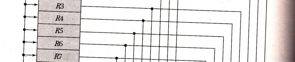
5 Computer Registers Register symbol DR AR AC IR PC TR INPR OUTR 8 No of bits Register name Function Data register Address register Accumulator Instruction register Program counter Temporary register Input register Output register Holds memory operand Holds address for memory Processor register Holds instruction i code Holds address of instruction Holds temporary data during processing Holds 8 bit character from an I/P device Holds 8 bit character for an O/P device
6 Comm mon Bus Syste em
7 Computer Instructions Instruction code formats Opcode Address Memory reference instruction Register operation Register reference instruction I/O operation Input output instruction Symbol Description INP OUT SKI SKO ION IOF Input character to AC Output character from AC Skip on input flag Skip on output flag Interrupt on Interrupt off
8 Symbol Description Cont AND ADD LDA STA BUN BSA ISZ CLA CLE CMA CME CIR CIL INC SPA SNA SZA SZE HLT AND memory word to AC ADD memory word to AC Load memory word to AC Store content of AC in memory Branch unconditionally Branch and save return address Increment and skip if zero Clear AC Clear E Complement AC Complement E Circulate right AC and E Circulate left AC and E Increment AC Skip next instruction if AC positive Skip next instruction if AC negative Skip next instruction if AC zero Skip next instruction if Ezero Halt computer
9 Cont Instructions are categorized into Arithmetic, logical, and shift instructions Instructions for moving information i to and from memory and processor registers Program control instructions together with instructions that check status conditions Input and output instructions
10 Timing and Control Timing for all registers is controlled by a master clock generator Control signals are generated in the control unit Two types of control organization: hardwired control and microprogrammed control Hardwired organization: control logic is implemented with gates, flip flops, decoders, d and other digital it circuits Microprogrammed organization: control information is stored in a control memory. This memory is programmed to initiate the required sequence of microoperations
11 Control Unit
12 D₃T₄: SC < 0 Control Timing Signal
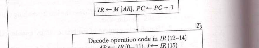
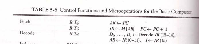
13 Instruction Cycle Fetch the instruction from the memory Decode the instruction Read effective address from memory if the instruction has an indirect address Execute the instruction Fetch and decode: Initially PC is loaded with address of the first instruction. SC is cleared to 0. After each clock pulse, SC is incremented by 1 so that timing signals go through the sequence T₀, T₁, T₂, and so on. microoperations T₀ : AR < PC T₁ : IR < M[AR], PC < PC + 1 T₂ : D₀,, D₇ < Decode IR(12 14), AR < IR(0 11), I < IR(15)

14


15 Determine the type of instruction in T₃
16 Register reference instructions use bits 0 to 11 to specify one of the 12 instructions ti These instructions are executed in T₃
17 Memory Reference Instructions Execution starts at T₄
18 Cont AND to AC D₀T₄ : DR < M[AR] D₀T₅ : AC < AC Λ DR, SC < 0 ADD to AC D₁T₄ : DR < M[AR] D₁T₅ : AC < AC + DR, E < C out, SC < 0 Output carry C out is transferred to E (extended accumulator) flip flop LDA D₂T₄ : DR < M[AR] D₂T₅ : AC < DR, SC < 0 STA D₃T₄ : M[AR] < AC, SC < 0
19 Cont Memory 0 BSA 135 BUN Next instruction D₄T₄ : PC < AR, SC < 0 BSA D₅T₄ : M[AR] < PC, AR < AR D₅T₅ : PC < AR, SC < 0 Subroutine ISZ D₆T₄ : DR < M[AR] D₆T₅ : DR < DR + 1 D₆T₆ : M[AR] < DR, if (DR = 0) then (PC < PC + 1), SC < 0 1 BUN 135


20
21 I/O Configuration I/O terminal Printer Serial communication interface Receiver interface Computer registers And flip flops FGO OUTR AC Keyboard Transmitter interface INPR Initially FGI is cleared to 0. When a key is struck in the keyboard, 8 bit alphanumeric code is shifted into INPR and FGI is set to 1. Then, the information from INPR is transferred in parallel to AC and FGI is cleared to 0 Initially FGO is set to 1. The information from AC is transferred din parallel to OUTR and FGO is cleared to 0. Printer accepts the information and prints it, and then sets FGO to 1 FGI
22 I/O Instructions D₇IT₃ = p (common to all I/O instructions) IR(i) = Bᵢ [bit in IR(6 11) that specifies the instruction) p SC < 0 Clear SC INP pb₁₁ AC(0 7) < INPR, FGI < 0 Input character OUT pb₁₀ OUTR < AC(0 7), FGO < 0 Output character SKI pb₉ If (FGI = 1) then (PC < PC + 1) Skip on input flag SKO pb₈ If (FGO = 1) then (PC < PC + 1) Skip on output flag ION pb₇ IEN < 1 Interrupt enable on IOF pb₆ IEN < 0 Interrupt enable off I/O instructions are used to transfer data to and from AC, to check flag bits and for controlling the interrupt facility


23 Interrupt Cycle
24 Memory Cont Memory BUN 1120 main program 255 PC = 256 PC = 1 0 BUN 1120 main program I/O program 1120 I/O program 1 BUN 0 1 BUN 0 Before interrupt After interrupt Register transfer statements Condition for setting flip flop R to 1 RT₀: AR < 0, TR < PC T₀ T₁ T₂ (IEN)(FGI + FGO): R < 1 RT₁: M[AR] < TR, PC < 0 RT₂: PC < PC + 1, IEN < 0, R < 0, SC < 0


25 Computer Components Memory unit Registers: AR, PC, DR, AC, IR, TR, OUTR, INPR, SC Flip flops: I, S, E, R, IEN, FGI, FGO Decoders: 3 x 8 operation decoder, 4 x 16 timing decoder 16 bit common bus Control logic gates Adder and logic circuit
26 aa


27 ss
28 Control of Registers Statements that change the contents of AR R T₀: AR < PC R T₂: AR < IR(0 11) D₇ IT₃: AR < M[AR] RT₀: AR < 0 D₅T₄: AR < AR + 1 Control I/P of registers LD(AR) = R T₀ + R T₂ + D₇ IT₃ CLR(AR) = RT₀ INR(AR) = D₅T₄ Read I/P Memory Read = R T₁ + D₇ IT₃ + (D₀ + D ₁+ D₂ + D₆)T₄
29 Control of Common Bus Encoder for bus selection circuit Inputs Outputs Register x₁ x₂ x₃ x₄ x₅ x₆ x₇ S₂ S₁ S₀ selected for bus None AR PC DR AC IR TR Memory


30 Control of Flip flops pb₇: IEN < 1 pb₆: IEN < 0 RT₂: IEN < 0 where p = D₇IT₃ and B₆ and B₇ are bits 6 and 7 of IR
31 Cont Boolean functions for the encoder S₀ = x₁ + x₃ + x₅ + x₇ S₁ = x₂ + x₃ + x₆ + x₇ S₂ = x₄ + x₅ + x₆ + x₇ Logic that makes x₁ = 1 (statements that have AR as source) D₄T₄ : PC < AR D₅T₅ : PC < AR Boolean function for x₁ x₁ = D₄T₄ + D₅T₅ x₁ x₂ x₃₃ x₄ x₅ x₆ x₇ Boolean function for x₇ (same as memory read) x₇ = R T₁ + D₇ IT₃ + (D₀ + D ₁+ D₂ + D₆)T₄ Encoder for bus selection inputs Encoder S₂₂ Multiplexer S₁ bus select S₀ inputs


 < E D₂T₅ :")
 < E pb₁₁ : AC(0 7) <")
32 Design of Accumulator Logic Register transfer statementsrb₁₁ : AC < 0 D₀T₅ ₀ ₅ : AC < AC Ʌ DR rb₉ ₉ : AC < AC D₁T₅ : AC < AC + DR rb₇ : AC < shr AC, AC(15) < E D₂T₅ : AC < DR rb₆ : AC < shl AC, AC(0) < E pb₁₁ : AC(0 7) < INPR rb₅ : AC < AC + 1
33

 are transferred to AC(0 15) Inputs of")

34 Adder & Logic Circuit Adder & logic circuit is divided into 16 stages, with each state corr: to one bit of AC When LD is enabled, 16 inputs Iᵢ (i = 0, 1,, 15) are transferred to AC(0 15) Inputs of the gates with symbolic names come from the outputs of gates marked with the same symbolic name in Fig 5.21
35 Microprogrammed control Function of a CU is to initiate a sequence of microoperations Methods of implementing a CU Hardwired control: control signals are generated by hardware Use of fixed instructions, fixed logic blocks of and/or arrays, encoder, decoderd High speed operation, expensive, relatively complex, no flexibility E.g. Intel 8085, Motorola 6802, Zilog 80, RISC CPUs Microprogrammed control: A CU whose binary control variables are stored in memory. An elegant and systematic method for controlling the microoperation sequences The control function that specifies a microoperation is a binary variable. Control variables are represented by control words. Each word in control memory (part of CU) contains a microinstruction. A sequence of microinstructions constitutes a microprogram E.g. Intel 8080, Motorola 68000, CISC CPUs
36 Cont Dynamic microprogramming permits a microprogram to be loaded from a magnetic disk Each machine instruction i initiates i i a series of microinstructions i i Microinstructions generate microoperations to fetch the instruction from main memory; to evaluate effective address, to execute the operation specified by the instruction, and to return control to the fetch phase to repeat the cycle for the next instruction Microinstruction contains bits for initiating microoperations and bits that determine the address sequence for the control memory Functions of microprogram sequencer : increment CAR by 1, load CAR with an address from control memory, transfer an external address, or load an initial address to start the control operations CAR (also called pipeline register) allows the execution of microoperations simultaneously with the generation of the next microinstruction Adv : The H/W configuration need not be changedfor different operations; instead specify a different set of microinstructions for control memory
37 Address sequencing Microinstructions are stored in groups (routine) Each computer instruction has its own microprogram routine to generate microoperations that execute the instruction An initial address is loaded into CAR when power is on. This address is the address of the first microinstruction that activates the instruction fetch routine. The fetch routine may be sequenced by incrementing CAR. At the end of the fetch routine, instruction is in IR Determine effective address of the operand addressing modes. This routine can be reached through a branch microinstruction, which is conditioned on the status of mode bits of the instruction. When this routine is completed, address of the operand is in MAR Generate microoperations to execute the instruction. Mapping a rule that transforms the instruction code into a control memory address. Microprograms that employ subroutines will Require an external register for storing the return address At the end of the execution of the instruction, return to fetch routine by executing an unconditional branch instruction


38 s
39 Cont Branch logic : Test the specified condition and branch to the indicated daddress if the condition is met; otherwise, CAR is incremented Status bits together with branch address in the microinstruction control the conditional branch decisions generated in the branch logic 3 bits in the microinstruction are used to specify any one of 8 status bit conditions. These bits provide selection variables for the multiplexer. If the selected status bit is in 1 state, o/p of the multiplexer is 1; otherwise 0. o/p 1 generates a control signal to transfer the branch address from the microinstruction into CAR. o/p 0 causes CAR to be incremented Status bits provide information such as carry out of an adder, sign bit of a number, mode bits of an instruction, and input/output status conditions
40 Mapping of Instruction 4 bit operation code should be converted into a 7 bit address for the control memory containing tii 128 words For each computer instruction, a microprogram routine may contain four microinstructions. If the routine needs more than 4 microinstructions, it can use addresses through If it uses fewer than four microinstructions, the unused memory locations would be available for other routines Subroutine: Microinstructions can be saved by employing subroutines that use common sections of microcode. E.g. sequence of microoperations needed to generate effective address of the operand Computer instruction opcode address Mapping bits 0 x x xx0 0 Microinstruction address
41
42 Computer Configuration Transfer of information among registers in the processor is done through MUX DR < AC, PC or memory AR < PC or DR PC < AR AC < ALU < AC, DR Memory receives its address from AR DR Memory
43 F3 Microoperation Symbol 000 None NOP 001 AC < AC DR XOR 010 AC < AC COM 011 AC < shl AC SHL 100 AC < shr AC SHR 101 PC < PC + 1 INCPC 110 PC < AR ARTPC 111 Reserved microinstruction : Two or more conflicting microoperations cannot be specified Microprogram Microinstruction format Condition for branching Address field F1(3) F2(3) F3(3) CD(2) BR(2) AD(7) Microoperation fields Branch field No more than 3 microoperations can be chosen for a microinstruction F1 Microoperation Symbol None AC < AC+ DR AC < 0 AC < AC + 1 AC < DR AR < DR (0 10) AR < PC M[AR] < DR NOP ADD CLRAC INCAC DRTAC DRTAR PCTAR WRITE F2 Microoperation Symbol None AC < AC DR AC < AC Ѵ DR AC < AC Λ DR DR < M[AR] DR < AC DR < DR + 1 DR (0 10) < PC NOP SUB OR AND READ ACTDR INCDR PCTDR
44 CD Condition Symbol Comments 00 Always =1 U Unconditional branch 01 DR (15) I Indirect address bit Cont AC (15) AC = 0 S Z Sign bit of AC Zero value in AC CD is used in conjunction with BR BR Symbol Function 00 JMP CAR < AD if condition = 1 01 CALL CAR < CAR + 1if condition = 0 CAR < AD, SBR < CAR + 1 if condition = 1 CAR < CAR + 1 if condition = RET MAP CAR < SBR (Return from subroutine) CAR (2 5) < DR (11 14), CAR (0, 1, 6) < 0 BR is used in conjunction with AD JMP and CALL instructions depend on CD RET and MAP are independent of CD and AD A symbolic (assembly language) microprogram is created using Symbols in the above tables AA symbolic microinstruction is divided into five fields: label, microoperations, CD, BR and AD Microoperations field consists of one, two or three symbols separated by commas. There may be no more than one symbol from each F field AD specifies the address in 3 ways 1. With symbolic address 2. NEXT 3. left empty for RET or MAP
45 Microinstructions for fetch routine AR < PC DR < M[AR], PC < PC + 1 AR < DR(0 10), CAR(2 5) < DR(11 14), CAR(0, 1, 6) < 0 Symbolic microprogram ORG 64 FETCH: PCTAR U JMP NEXT READ, INCPC U JMP NEXT DRTAR U MAP Binary microprogram Binary F1 F2 F3 CD BR AD address Cont
46 Symbolic Microprogram (Partial) Label Microoperations CD BR AD ADD: ORG 0 NOP READ ADD I U U CALL JMP JMP INDRCT NEXT FETCH Cont BRANCH: OVER: ORG 4 NOP NOP NOP ARTPC S U I U JMP JMP CALL JMP OVER FETCH INDRCT FETCH STORE: ORG 8 NOP ACTDR WRITE I U U CALL JMP JMP INDRCT NEXT FETCH EXCHANGE: ORG 12 NOP READ ACTDR, DRTAC WRITE I U U U CALL JMP JMP JMP INDRCT NEXT NEXT FETCH
47 Cont FETCH: INDRCT: ORG 64 PCTAR U JMP NEXT READ, INCPC U JMP NEXT DRTAR U MAP READ U JMP NEXT DRTAR U RET The various fields in microinstruction format provide control bits to initiate The various fields in microinstruction format provide control bits to initiate microoperations in the system. Each field requires a decoder to produce the corresponding control signals


48 Design of Control Unit
49 Microprogram Sequencer Basic components of μp CU: control memory, circuits that select next address The addressselectionselection part is called microprogram sequencer Purpose: To present an address to the CM so that a MI may be read and executed The next addresslogic of the sequencerdetermines the specific address source to be loaded into CAR. The choice of address source is guided by the next address information bits that the sequencer receives from the present MI CD field of MI selects one of the status bits in MUX2. If this bit is 1, T (test) variable is 1; otherwise 0 T value together with 2 bits of BR field will go to input logic circuit. The input logic will determine the type of operations (increment, branch or jump, call and return from subroutine, load an external address, push or pop the stack, and other address sequencing operations) that are available in the unit A sequencer will have a register stack of about 4 to 8 levels deep. So a number of subroutines can be active at the same time


50
51 Cont Boolean functions for input logic circuit S₁ = I₁ S₀ = I₁I₀ + I₁ T L = I₁ I₀T Input logic truth table BR field Input MUX 1 Load SBR I₁ I₀ T S₁ S₀ L X X 1 1 0


52 CPU
53 R1 < R2 R3 Cont Field : SELA SELB SELD OPR Symbol : R2 R3 R1 SUB Control word : ALU operations OPR Operation Symbol Transfer A TSFA Increment A Add A + B Subtract A B INCA ADD SUB Decrement A AND A and B OR A and B XOR A and B Complement A Shift right A Shift left A DECA AND OR XOR COMA SHRA SHLA
54 Cont
55 Stack Organisation Stack works on LIFO basis SP always points at the top item in the stack FULL EMTY SP contains 6 bits FULL is set when stack is full, and EMTY is set when stack is empty DR holds the data dt to be written into or read out of the stack Push: SP < SP + 1 M[SP] < DR 4 If (SP = 0) then FULL < 1 SP C 3 EMTY < 0 B 2 First item is stored at location 1, and the last A item at 0 1 Pop: DR < M[SP] 0 SP < SP 1 If (SP = 0) then EMTY < 1 DR FULL < 0 64 word register stack Address 63
56 Cont Push: SP < SP 1 M[SP] < DR Pop: DR < M[SP] SP < SP + 1 Two registers are used to check the limits of the stack Stack organisation is very effective for evaluating arithmetic ti expressions Reverse polish notation (postfix) is suitable for stack manipulation Infix: A * B + C * D Postfix: AB * CD *+ PC Memory unit Program (instructions) 1000 AR Data 2000 (operands) Stack SP DR
57 Instruction Formats Consists of opcode field, address field and mode field CPU organisations Single accumulator organization ADD X AC < AC + M[X] General register organisation ADD R1, R2, R3 R1 < R2 + R3 ADD R1, R2 R1 < R1 + R2 ADD R1, X R1 < R1 + M[X] Stack orgaisation PUSH X ADD
58 Cont X = (A + B) * (C + D) Three address instructions ADD R1, A, B R1 < M[A] + M[B] ADD R2, C, D R2 < M[C] + M[D] MUL X, R1, R2 M[X] < R1 * R2 Computer : Cyber 170 Two address instruction MOV R1, A R1 < M[A] ADD R1, B R1 < R1 + M[B] MOV R2, C R2 < M[C] ADD R2, D R1 < R2 + M[D] MUL R1, R2 R1 < R1 * R2 MOV X, R1 M[X] < R1
59 One address instruction Cont LOAD A AC < M[A] ADD B AC < AC + M[B] STORE T M[T] < AC LOAD C AC < M[C] ADD D AC < AC + M[D] MUL T AC < AC * M[T] [] STORE X M[X] < AC Zero address instruction PUSH A TOS < A PUSH B TOS < B ADD TOS < (A + B) PUSH C TOS < C PUSH D TOS < D ADD TOS < (C + D) MUL TOS < (C + D) * (A + B) POP X M[X] < TOS RISC instruction LOAD R1, A LOAD R2, B LOAD R3, C LOAD R4, D ADD R1, R1, R2 ADD R3, R3, R4 MUL R1, R1, R3 STORE X, R1 R1 < M[A] R2 < M[B] R3 < M[C] R4 < M[D] R1 < R1 + R2 R3 < R3 + R4 R1 < R1 * R3 M[X] < R1
60 Addressing Modes Instruction cycle Fetch the instruction from the memory: PC points towards the address of the next instruction to be executed Decode the instruction: Determine the operation to be performed, addressing mode of the instruction, and the location of the operands Execute the instruction Implied mode: operands are implicit in the instructions E.g. complement accumulator, zero address instructions Immediate mode: operand is specified in the instruction itself Register mode: operandsareare in registers Register indirect mode: address of the operand is in register Autoincrement or autodecrement mode: register is incremented or decremented after its value is used to access the memory
61 Cont Direct address mode: address is specified in the instruction Indirect address mode: address of the effective address is given in the instruction Relative address mode: effective address = address part of the instruction + content of PC Indexed daddressing mode: effective address = address part of the instruction + content of index register Base register addressing mode: effective address = address part of the instruction + content of base register EgLoad E.g AC with a value
62 Computer Instructions Data transfer Instructions Name Load Store Move Exchange Input Output Push Pop Mnemonics LD ST MOV XCH IN OUT PUSH POP
63 Data Manipulation Instructions ADDI : add two binary integers ADDF : add two floating point numbers ADDD : add two decimal numbers in BCD Name Increment Decrement Add Subtract Multiply Divide Add with carry Subtract with borrow Negate (2 s complement) Mnemonic INC DEC ADD SUB MUL DIV ADDC SUBB NEG
64 Cont Logical and bit manipulation instructions Name Clear Complement AND OR Exclusive OR Clear carry Set carry Complement carry Enable interrupt Disable interrupt Mnemonic CLR COM AND OR XOR CLRC SETC COMC EI DI
65 Cont Shift instructions OP REG TYPE RL COUNT Name Logical shift right Logical shift left Arithmetic shift right Arithmetic shift left Rotate right Rotate left Rotate right through carry Rotate left through carry Mnemonic SHR SHL SHRA SHLA ROR ROL RORC ROLC
66 Program Control Instructions may alter the flow of control Conditional and unconditional branch and jump instructions SKP (zero address) instruction skips the next instruction Certain status bits are set as a result of compare and test (performs logical AND) operations Name Branch Jump Skip Call Return Compare (by subtraction) ti Test (by ANDing) Mnemonic BR JMP SKP CALL RET CMP TST
67 Cont Status bits : Carry, Sign, Zero, overflow
68 Mnemonic Branch condition Tested condition BZ BNZ BC BNC BP BM BV BNV BHI BHE BLO BLOE BE BNE BGT BGE BLT BLE BE BNE Branch if zero Branch if not zero Z = 1 Z = 0 Branch if carry C = 1 Branch if no carry C = 0 Branch if plus S = 0 Branch if minus S = 1 Branch if overflow V= 1 Branch if no overflow V = 0 Unsigned compare conditions (A B) Branch if higher Branch if higher or equal Branch if lower Branch if lower or equal Branch if equal Branch if not equal A > B A B A < B A B A = B A B Signed compare conditions (A B) Branch if greater than Branch if greater or equal Branch if less than Branch if less or equal Branch if equal Branch if not equal A > B A B A<B A B A = B A B Cont Conditional Branch instructions
69 Cont Microoperations in a subroutine call SP < SP 1 M[SP] < PC PC < effective address Microoperations in a return statement PC < M[SP] SP < SP + 1
70 Program interrupt: refers to the transfer of program control from a currently running program to another service program as a result of an external or internal request Interrupt Interrupt procedure: interrupt is usually initiated by an external or internal signal Address of the interrupt service program is determined by the h/w Interrupt procedure stores all the information necessary to define the state of the CPU Content of program counter, registers and certain status conditions PSW (stored in a register) : collection of all status bit conditions. It includes status bits from the last ALU operation, interrupts that are allowed to occur, whether the CPU is in supervisor or user mode Types of Interrupts External interrupts : come from I/O devices, from a timing device, from a circuit monitoring the power supply, or from any other external source Internal interrupts (traps) : arise from illegal or erroneous use of an instruction or date. E.g. register overflow, stack overflow, divide by zero, invalid opcode, protection violation Software interrupt : programmer initiates the interrupt by executing a special call instruction. It is used to switch from user mode to supervisor mode
Computer Architecture
 http://www.bsccsit.com/ Computer Architecture CSC. 201 Third Semester Prepared By: Arjun Singh Saud Special thanks to Mr. Arjun Singh Saud for providing this valuable note! Chapter 1 Data representation
BASIC COMPUTER ORGANIZATION AND DESIGN
 1 BASIC COMPUTER ORGANIZATION AND DESIGN Instruction Codes Computer Registers Computer Instructions Timing and Control Instruction Cycle Memory Reference Instructions Input-Output and Interrupt Complete
TYPES OF INTERRUPTS: -
 There are 3 types of interrupts. TYPES OF INTERRUPTS: - External Interrupts. Internal Interrupts. Software interrupts. Hardware Interrupts (1) External interrupts come from I/O devices, from a timing device
BASIC COMPUTER ORGANIZATION AND DESIGN
 1 BASIC COMPUTER ORGANIZATION AND DESIGN Instruction Codes Computer Registers Computer Instructions Timing and Control Instruction Cycle Memory Reference Instructions Input-Output and Interrupt Complete
5-1 Instruction Codes
 Chapter 5: Lo ai Tawalbeh Basic Computer Organization and Design 5-1 Instruction Codes The Internal organization of a digital system is defined by the sequence of microoperations it performs on data stored
BASIC COMPUTER ORGANIZATION AND DESIGN
 BASIC COMPUTER ORGANIZATION AND DESIGN Instruction Codes Computer Registers Computer Instructions Timing and Control Instruction Cycle Memory Reference Instructions Input-Output and Interrupt Complete
Basic Computer Organization - Designing your first computer. Acknowledgment: Most of the slides are adapted from Prof. Hyunsoo Yoon s slides.
 Basic Computer Organization - Designing your first computer Acknowledgment: Most of the slides are adapted from Prof. Hyunsoo Yoon s slides. 1 This week- BASIC COMPUTER ORGANIZATION AND DESIGN Instruction
CHAPTER 5 Basic Organization and Design Outline Instruction Codes Computer Registers Computer Instructions Timing and Control Instruction Cycle
 CS 224: Computer Organization S.KHABET CHAPTER 5 Basic Organization and Design Outline Instruction Codes Computer Registers Computer Instructions Timing and Control Instruction Cycle Memory Reference Instructions
Computer Organization (Autonomous)
") Computer Organization (Autonomous) UNIT II Sections - A & D Prepared by Anil Kumar Prathipati, Asst. Prof., Dept. of CSE. SYLLABUS Basic Computer Organization and Design: Instruction codes Stored Program
Computer Organization (Autonomous) UNIT II Sections - A & D Prepared by Anil Kumar Prathipati, Asst. Prof., Dept. of CSE. SYLLABUS Basic Computer Organization and Design: Instruction codes Stored Program
csitnepal Unit 3 Basic Computer Organization and Design
 Unit 3 Basic Computer Organization and Design Introduction We introduce here a basic computer whose operation can be specified by the resister transfer statements. Internal organization of the computer
Basic Computer Organization and Design Part 2/3
 Basic Computer Organization and Design Part 2/3 Adapted by Dr. Adel Ammar Computer Organization Basic Computer Instructions Basic Computer Instruction Format Memory-Reference Instructions (OP-code = 000
Fig: Computer memory with Program, data, and Stack. Blog - NEC (Autonomous) 1
 1") Central Processing Unit 1. Stack Organization A useful feature that is included in the CPU of most computers is a stack or last in, first out (LIFO) list. A stack is a storage device that stores information
Central Processing Unit 1. Stack Organization A useful feature that is included in the CPU of most computers is a stack or last in, first out (LIFO) list. A stack is a storage device that stores information
COMPUTER ORGANIZATION
 COMPUTER ORGANIZATION INDEX UNIT-II PPT SLIDES Srl. No. Module as per Session planner Lecture No. PPT Slide No. 1. Register Transfer language 2. Register Transfer Bus and memory transfers 3. Arithmetic
UNIT:2 BASIC COMPUTER ORGANIZATION AND DESIGN
 1 UNIT:2 BASIC COMPUTER ORGANIZATION AND DESIGN BASIC COMPUTER ORGANIZATION AND DESIGN 2.1 Instruction Codes 2.2 Computer Registers AC or Accumulator, Data Register or DR, the AR or Address Register, program
Chapter 5. Computer Architecture Organization and Design. Computer System Architecture Database Lab, SANGJI University
 Chapter 5. Computer Architecture Organization and Design Computer System Architecture Database Lab, SANGJI University Computer Architecture Organization and Design Instruction Codes Computer Registers
Introduction. 3 major parts of CPU : Fig Design Examples of simple CPU. In this chapter : Chap. 8. Chap. 8 Central Processing Unit
 Central Processing Unit 8-1 Introduction 3 major parts of CPU : Fig. 8-1 1) Register Set 2) ALU 3) Control Design Examples of simple CPU Hardwired Control : Chap. 5 Microprogrammed Control : Chap. 7 In
10-1 C D Pearson Education, Inc. M. Morris Mano & Charles R. Kime LOGIC AND COMPUTER DESIGN FUNDAMENTALS, 4e
 10-1 C D E A B 10-2 A B A B C (A B) C D A A B (A B) C E D (A B) C D E (A B) C + D E (A B) C 10-3 Opcode Mode Address or operand 10-4 Memory 250 Opcode Mode PC = 250 251 ADRS 252 Next instruction ACC Opcode:
TABLE 9-1. Symbolic Convention for Addressing Modes. Register indirect LDA (R1) ACC M[ R1] Refers to Figure 9-4. Addressing mode. Symbolic convention
![TABLE 9-1. Symbolic Convention for Addressing Modes. Register indirect LDA (R1) ACC M[ R1] Refers to Figure 9-4. Addressing mode. Symbolic convention](/thumbs/78/77835871.jpg "TABLE 9-1. Symbolic Convention for Addressing Modes. Register indirect LDA (R1) ACC M[ R1] Refers to Figure 9-4. Addressing mode. Symbolic convention") T-236 Symbolic Convention for Addressing Modes TABLE 9-1 Symbolic Convention for Addressing Modes Refers to Figure 9-4 Addressing mode Symbolic convention Register transfer Effective address Contents of
T-236 Symbolic Convention for Addressing Modes TABLE 9-1 Symbolic Convention for Addressing Modes Refers to Figure 9-4 Addressing mode Symbolic convention Register transfer Effective address Contents of
Computer Architecture and Organization: L06: Instruction Cycle
 Computer Architecture and Organization: L06: Instruction Cycle By: A. H. Abdul Hafez Abdul.hafez@hku.edu.tr, ah.abdulhafez@gmail.com 1 Outlines 1. Fetch and decode 2. Determine the Type of Instruction
CHAPTER 8: Central Processing Unit (CPU)
") CS 224: Computer Organization S.KHABET CHAPTER 8: Central Processing Unit (CPU) Outline Introduction General Register Organization Stack Organization Instruction Formats Addressing Modes 1 Major Components
CS 224: Computer Organization S.KHABET CHAPTER 8: Central Processing Unit (CPU) Outline Introduction General Register Organization Stack Organization Instruction Formats Addressing Modes 1 Major Components
Computer Organization and Design
 CSE211 Computer Organization and Design Lecture : 3 Tutorial: 1 Practical: 0 Credit: 4 KIDS Labs 1 Unit 1 : Basics of Digital Electronics Introduction Logic Gates Flip Flops Decoder Encoder Multiplexers
Computer Architecture Programming the Basic Computer
 4. The Execution of the EXCHANGE Instruction The EXCHANGE routine reads the operand from the effective address and places it in DR. The contents of DR and AC are interchanged in the third microinstruction.
COMPUTER HARDWARE. Instruction Set Architecture
 COMPUTER HARDWARE Instruction Set Architecture Overview Computer architecture Operand addressing Addressing architecture Addressing modes Elementary instructions Data transfer instructions Data manipulation
CHAPTER SIX BASIC COMPUTER ORGANIZATION AND DESIGN
 CHAPTER SIX BASIC COMPUTER ORGANIZATION AND DESIGN 6.1. Instruction Codes The organization of a digital computer defined by: 1. The set of registers it contains and their function. 2. The set of instructions
Blog - https://anilkumarprathipati.wordpress.com/
 Control Memory 1. Introduction The function of the control unit in a digital computer is to initiate sequences of microoperations. When the control signals are generated by hardware using conventional
UNIT-II. Part-2: CENTRAL PROCESSING UNIT
 Page1 UNIT-II Part-2: CENTRAL PROCESSING UNIT Stack Organization Instruction Formats Addressing Modes Data Transfer And Manipulation Program Control Reduced Instruction Set Computer (RISC) Introduction:
Darshan Institute of Engineering & Technology for Diploma Studies Unit - 1
 Darshan Institute of Engineering & Technology for Diploma Studies Unit - 1 1. Draw and explain 4 bit binary arithmetic or adder circuit diagram. A binary parallel adder is digital function that produces
Unit II Basic Computer Organization
 1. Define the term. Internal Organization-The internal organization of a digital system is defined by the sequence of microoperations it performs on data stored in its registers. Program- A program is
MICROPROGRAMMED CONTROL:-
 MICROPROGRAMMED CONTROL:- Two methods of implementing control unit are Hardwired Control & Micro-Programmed Control. Hardwired: - when the control signals are generated by hardware using conventional logic
CENTRAL PROCESSING UNIT
 1 CENTRAL PROCESSING UNIT Introduction General Register Organization Stack Organization Instruction Formats Addressing Modes Data Transfer and Manipulation Program Control Reduced Instruction Set Computer
MICROPROGRAMMED CONTROL
 1 MICROPROGRAMMED CONTROL Control Memory Sequencing Microinstructions Microprogram Example Design of Control nit Microinstruction Format Nanostorage and Nanoprogram 2 Implementation of Control nit COMPARISON
Chapter 3 : Control Unit
 3.1 Control Memory Chapter 3 Control Unit The function of the control unit in a digital computer is to initiate sequences of microoperations. When the control signals are generated by hardware using conventional
Computer Architecture
 Computer Architecture Lecture 1: Digital logic circuits The digital computer is a digital system that performs various computational tasks. Digital computers use the binary number system, which has two
CENTRAL PROCESSING UNIT
 1 CENTRAL PROCESSING UNIT Introduction General Register Organization Stack Organization Instruction Formats Addressing Modes Data Transfer and Manipulation Program Control Reduced Instruction Set Computer
Blog -
 . Instruction Codes Every different processor type has its own design (different registers, buses, microoperations, machine instructions, etc) Modern processor is a very complex device It contains Many
MICROPROGRAMMED CONTROL
 MICROPROGRAMMED CONTROL Hardwired Control Unit: When the control signals are generated by hardware using conventional logic design techniques, the control unit is said to be hardwired. Micro programmed
MICROPROGRAMMED CONTROL
 1 MICROPROGRAMMED CONTROL Control Memory Sequencing Microinstructions Microprogram Example Design of Control nit Microinstruction Format Nanostorage and Nanoprogram External input (IR) Next address generator
MICROPROGRAMMED CONTROL
 1 MICROPROGRAMMED CONTROL Control Memory Sequencing Microinstructions Microprogram Example Design of Control nit Microinstruction Format Nanostorage and Nanoprogram 2 Implementation of Control nit COMPARISON
Control Unit Implementation Hardwired Memory
 Chapter 7: Microprogrammed nit mplementation Hardwired nstruction code Sequence Counter Combinational Logic Circuits signals Microprogrammed nstruction code CAR: Register CDR: Data Register Next Generator
Programming Level A.R. Hurson Department of Computer Science Missouri University of Science & Technology Rolla, Missouri
 Programming Level A.R. Hurson Department of Computer Science Missouri University of Science & Technology Rolla, Missouri 65409 hurson@mst.edu A.R. Hurson 1 Programming Level Computer: A computer with a
COMPUTER ARCHITECTURE AND ORGANIZATION Register Transfer and Micro-operations 1. Introduction A digital system is an interconnection of digital
 Register Transfer and Micro-operations 1. Introduction A digital system is an interconnection of digital hardware modules that accomplish a specific information-processing task. Digital systems vary in
Nanostorage and Nanoprogram
 Computer System AA rc hh ii tec ture (7 ) Nanostorage and Nanoprogram 2 Combinational Logic Circuits (Hard-wired) Microprogram 3 Microprogram - - Microinstruction - - - - Control Memory(Control Storage:
STRUCTURE OF DESKTOP COMPUTERS
 Page no: 1 UNIT 1 STRUCTURE OF DESKTOP COMPUTERS The desktop computers are the computers which are usually found on a home or office desk. They consist of processing unit, storage unit, visual display
Midterm Examination # 2 Wednesday, March 18, Duration of examination: 75 minutes
 Page 1 of 8 School of Computer Science 60-265-01 Computer Architecture and Digital Design Winter 2009 Midterm Examination # 2 Wednesday, March 18, 2009 Student Name: First Name Family Name Student ID Number:
Class Notes. Dr.C.N.Zhang. Department of Computer Science. University of Regina. Regina, SK, Canada, S4S 0A2
 Class Notes CS400 Part VI Dr.C.N.Zhang Department of Computer Science University of Regina Regina, SK, Canada, S4S 0A2 C. N. Zhang, CS400 83 VI. CENTRAL PROCESSING UNIT 1 Set 1.1 Addressing Modes and Formats
CPU Design John D. Carpinelli, All Rights Reserved 1
 CPU Design 1997 John D. Carpinelli, All Rights Reserved 1 Outline Register organization ALU design Stacks Instruction formats and types Addressing modes 1997 John D. Carpinelli, All Rights Reserved 2 We
COMPUTER ARCHITECTURE AND PARALEL PROCESSING STUDY NOTES
 COMPUTER ARCHITECTURE AND PARALEL PROCESSING STUDY NOTES UNIT 1 INTRODUCTION Central Processing unit (CPU): Alternately referred to as a processor, central processor, or microprocessor, the CPU is the
Chap. 7 Microprogrammed Control(Control Unit)
") (Control Unit) 7-1 7-1 Control Memory Control Unit Initiate sequences of microoperations» Control signal (that specify microoperations) in a bus-organized system groups of bits that select the paths in
(Control Unit) 7-1 7-1 Control Memory Control Unit Initiate sequences of microoperations» Control signal (that specify microoperations) in a bus-organized system groups of bits that select the paths in
IAS Computer. Instructions
 IAS Computer Instructions The IAS computer was designed in the 1940's and built in the early 1950's by John von Neumann at the Princeton Institute for Advanced Studies. It can arguably be called the father
Introduction. Machine Language. Assembly Language. Assembler. Program Loops. Programming Arithmetic and Logic Operations.
 Computer System AA rc hh ii tec ture( 66 )) PROGRAMMING THE BASIC COMPUTER Introduction Machine Language Assembly Language Assembler Program Loops Programming Arithmetic and Logic Operations Subroutines
REGISTER TRANSFER LANGUAGE
 REGISTER TRANSFER LANGUAGE The operations executed on the data stored in the registers are called micro operations. Classifications of micro operations Register transfer micro operations Arithmetic micro
COMPUTER ARCHITECTURE AND DIGITAL DESIGN
 SPECIAL MAKEUP - FINAL EXAMINATION COMPUTER ARCHITECTURE AND DIGITAL DESIGN 03-60-265-01 S C H O O L O F C O M P U T E R S C I E N C E - U N I V E R S I T Y O F W I N D S O R Fall 2008 Last Name: First
Computer Architecture and Organization: L09: CPU Organization
 Computer Architecture and Organization: L09: CPU Organization By: A. H. Abdul Hafez Abdul.hafez@hku.edu.tr, ah.abdulhafez@gmail.com, hafez@research.iiit.ac.in 1 CAO, by Dr. A.H. Abdul Hafez, CE Dept. HKU
Computer architecture Assignment 3
 Computer architecture Assignment 3 1- An instruction at address 14E in the basic computer has I=0, an operation code of the AND instruction, and an address part equal to 109(all numbers are in hexadecimal).
TYPICAL QUESTIONS & ANSWERS
 TYPICAL QUESTIONS & ANSWERS PART-I Each Question carries 2 marks. OBJECTIVE TYPE QUESTIONS Choose the correct or best alternative in the following: Q.1 In Reverse Polish notation, expression A*B+C*D is
UNIT - V MEMORY P.VIDYA SAGAR ( ASSOCIATE PROFESSOR) Department of Electronics and Communication Engineering, VBIT
 Department of Electronics and Communication Engineering, VBIT") UNIT - V MEMORY P.VIDYA SAGAR ( ASSOCIATE PROFESSOR) contents Memory: Introduction, Random-Access memory, Memory decoding, ROM, Programmable Logic Array, Programmable Array Logic, Sequential programmable
UNIT - V MEMORY P.VIDYA SAGAR ( ASSOCIATE PROFESSOR) contents Memory: Introduction, Random-Access memory, Memory decoding, ROM, Programmable Logic Array, Programmable Array Logic, Sequential programmable
THE MICROPROCESSOR Von Neumann s Architecture Model
 THE ICROPROCESSOR Von Neumann s Architecture odel Input/Output unit Provides instructions and data emory unit Stores both instructions and data Arithmetic and logic unit Processes everything Control unit
CHETTINAD COLLEGE OF ENGINEERING AND TECHNOLOGY COMPUTER ARCHITECURE- III YEAR EEE-6 TH SEMESTER 16 MARKS QUESTION BANK UNIT-1
 CHETTINAD COLLEGE OF ENGINEERING AND TECHNOLOGY COMPUTER ARCHITECURE- III YEAR EEE-6 TH SEMESTER 16 MARKS QUESTION BANK UNIT-1 Data representation: (CHAPTER-3) 1. Discuss in brief about Data types, (8marks)
CHAPTER SEVEN PROGRAMMING THE BASIC COMPUTER
 CHAPTER SEVEN 71 Introduction PROGRAMMING THE BASIC COMPUTER A computer system as it was mentioned before in chapter 1, it is subdivided into two functional parts: 1 Hardware, which consists of all physical
C.P.U Organization. Memory Unit. Central Processing Unit (C.P.U) Input-Output Processor (IOP) Figure (1) Digital Computer Block Diagram
 Input-Output Processor (IOP) Figure (1) Digital Computer Block Diagram") C.P.U Organization 1.1 Introduction A computer system is sometimes subdivided into two functional entities "Hardware" and "Software". The H/W of the computer consists of all the electronic components and
C.P.U Organization 1.1 Introduction A computer system is sometimes subdivided into two functional entities "Hardware" and "Software". The H/W of the computer consists of all the electronic components and
Assembly Language Programming of 8085
 Assembly Language Programming of 8085 Topics 1. Introduction 2. Programming model of 8085 3. Instruction set of 8085 4. Example Programs 5. Addressing modes of 8085 6. Instruction & Data Formats of 8085
UNIT-III REGISTER TRANSFER LANGUAGE AND DESIGN OF CONTROL UNIT
 UNIT-III 1 KNREDDY UNIT-III REGISTER TRANSFER LANGUAGE AND DESIGN OF CONTROL UNIT Register Transfer: Register Transfer Language Register Transfer Bus and Memory Transfers Arithmetic Micro operations Logic
(2) Explain the addressing mode of OR What do you mean by addressing mode? Explain diff. addressing mode for 8085 with examples.
 Explain the addressing mode of OR What do you mean by addressing mode? Explain diff. addressing mode for 8085 with examples.") (1) Explain instruction format and Opcode format of 8085 μp with example. OR With help of examples, explain the formation of opcodes of 8085 OR What is an instruction? List type of instruction based on
(1) Explain instruction format and Opcode format of 8085 μp with example. OR With help of examples, explain the formation of opcodes of 8085 OR What is an instruction? List type of instruction based on
2 MARKS Q&A 1 KNREDDY UNIT-I
 2 MARKS Q&A 1 KNREDDY UNIT-I 1. What is bus; list the different types of buses with its function. A group of lines that serves as a connecting path for several devices is called a bus; TYPES: ADDRESS BUS,
 Instruction Set Instruction set of 8085 can be classified in following groups: Data Transfer Instructions These instructions can perform data transfer operations between Registers of 8085 e.g. MOV 8085
Architecture & Instruction set of 8085 Microprocessor and 8051 Micro Controller
 of 8085 microprocessor 8085 is pronounced as "eighty-eighty-five" microprocessor. It is an 8-bit microprocessor designed by Intel in 1977 using NMOS technology. It has the following configuration 8-bit
Computer Organization Control Unit. Department of Computer Science Missouri University of Science & Technology
 Control Unit Department of Computer Science Missouri University of Science & Technology hurson@mst.edu 1 Note, this unit will be covered in three lectures. In case you finish it earlier, then you have
Computer Organization CS 206 T Lec# 2: Instruction Sets
 Computer Organization CS 206 T Lec# 2: Instruction Sets Topics What is an instruction set Elements of instruction Instruction Format Instruction types Types of operations Types of operand Addressing mode
8051 Overview and Instruction Set
 8051 Overview and Instruction Set Curtis A. Nelson Engr 355 1 Microprocessors vs. Microcontrollers Microprocessors are single-chip CPUs used in microcomputers Microcontrollers and microprocessors are different
COA. Prepared By: Dhaval R. Patel Page 1. Q.1 Define MBR.
 Q.1 Define MBR. MBR( Memory buffer register) A Memory Buffer Register (MBR) is the register in a computers processor that stores the data being transferred to and from the devices It allowing the processor
Module 5 - CPU Design
 Module 5 - CPU Design Lecture 1 - Introduction to CPU The operation or task that must perform by CPU is: Fetch Instruction: The CPU reads an instruction from memory. Interpret Instruction: The instruction
The Assembly Language of the Boz 5
 The Assembly Language of the Boz 5 The Boz 5 uses bits 31 27 of the IR as a five bit opcode. Of the possible 32 opcodes, only 26 are implemented. Op-Code Mnemonic Description 00000 HLT Halt the Computer
Register Transfer and Micro-operations
 Register Transfer Language Register Transfer Bus Memory Transfer Micro-operations Some Application of Logic Micro Operations Register Transfer and Micro-operations Learning Objectives After reading this
Faculty of Engineering Systems & Biomedical Dept. First Year Cairo University Sheet 6 Computer I
 aculty of Engineering Systems & Biomedical Dept. irst Year Cairo University Sheet 6 Computer I 1. Choose rue or alse for each of the following statements a) In a direct addressing mode instruction, the
Computer Organization and Technology Processor and System Structures
 Computer Organization and Technology Processor and System Structures Assoc. Prof. Dr. Wattanapong Kurdthongmee Division of Computer Engineering, School of Engineering and Resources, Walailak University
Digital System Design Using Verilog. - Processing Unit Design
 Digital System Design Using Verilog - Processing Unit Design 1.1 CPU BASICS A typical CPU has three major components: (1) Register set, (2) Arithmetic logic unit (ALU), and (3) Control unit (CU) The register
M. Sc (CS) (II Semester) Examination, Subject: Computer System Architecture Paper Code: M.Sc-CS-203. Time: Three Hours] [Maximum Marks: 60
![M. Sc (CS) (II Semester) Examination, Subject: Computer System Architecture Paper Code: M.Sc-CS-203. Time: Three Hours] [Maximum Marks: 60](/thumbs/87/96339673.jpg "M. Sc (CS) (II Semester) Examination, Subject: Computer System Architecture Paper Code: M.Sc-CS-203. Time: Three Hours] [Maximum Marks: 60") M. Sc (CS) (II Semester) Examination, 2012-13 Subject: Computer System Architecture Paper Code: M.Sc-CS-203 Time: Three Hours] [Maximum Marks: 60 Note: Question Number 1 is compulsory. Answer any four
M. Sc (CS) (II Semester) Examination, 2012-13 Subject: Computer System Architecture Paper Code: M.Sc-CS-203 Time: Three Hours] [Maximum Marks: 60 Note: Question Number 1 is compulsory. Answer any four
COMPUTER ORGANIZATION & ARCHITECTURE
 COMPUTER ORGANIZATION & ARCHITECTURE Instructions Sets Architecture Lesson 5a 1 What are Instruction Sets The complete collection of instructions that are understood by a CPU Can be considered as a functional
INSTRUCTION SET OF 8085
 INSTRUCTION SET OF 8085 Instruction Set of 8085 An instruction is a binary pattern designed inside a microprocessor to perform a specific function. The entire group of instructions that a microprocessor
8085 INSTRUCTION SET INSTRUCTION DETAILS
 8085 INSTRUCTION SET INSTRUCTION DETAILS DATA TRANSFER INSTRUCTIONS MOV Rd, Rs Copy from source to destination This instruction copies the contents of the source register Rs into the destination register
REGISTER TRANSFER AND MICROOPERATIONS
 1 REGISTER TRANSFER AND MICROOPERATIONS Register Transfer Language Register Transfer Bus and Memory Transfers Arithmetic Microoperations Logic Microoperations Shift Microoperations Arithmetic Logic Shift
COMPUTER ORGANIZATION AND ARCHITECTURE
 Page 1 1. Which register store the address of next instruction to be executed? A) PC B) AC C) SP D) NONE 2. How many bits are required to address the 128 words of memory? A) 7 B) 8 C) 9 D) NONE 3. is the
Micro-Operations. execution of a sequence of steps, i.e., cycles
 Micro-Operations Instruction execution execution of a sequence of steps, i.e., cycles Fetch, Indirect, Execute & Interrupt cycles Cycle - a sequence of micro-operations Micro-operations data transfer between
The von Neumann Architecture. IT 3123 Hardware and Software Concepts. The Instruction Cycle. Registers. LMC Executes a Store.
 IT 3123 Hardware and Software Concepts February 11 and Memory II Copyright 2005 by Bob Brown The von Neumann Architecture 00 01 02 03 PC IR Control Unit Command Memory ALU 96 97 98 99 Notice: This session
REGISTER TRANSFER AND MICROOPERATIONS
 REGISTER TRANSFER AND MICROOPERATIONS Register Transfer Language Register Transfer Bus and Memory Transfers Arithmetic Microoperations Logic Microoperations Shift Microoperations Arithmetic Logic Shift
Combinational and sequential circuits (learned in Chapters 1 and 2) can be used to create simple digital systems.
 can be used to create simple digital systems.") REGISTER TRANSFER AND MICROOPERATIONS Register Transfer Language Register Transfer Bus and Memory Transfers Arithmetic Microoperations Logic Microoperations Shift Microoperations Arithmetic Logic Shift
REGISTER TRANSFER AND MICROOPERATIONS Register Transfer Language Register Transfer Bus and Memory Transfers Arithmetic Microoperations Logic Microoperations Shift Microoperations Arithmetic Logic Shift
CHAPTER 4: Register Transfer Language and Microoperations
 CS 224: Computer Organization S.KHABET CHAPTER 4: Register Transfer Language and Microoperations Outline Register Transfer Language Register Transfer Bus and Memory Transfers Arithmetic Microoperations
CSCI 2121 Computer Organization and Assembly Language PRACTICE QUESTION BANK
 CSCI 2121 Computer Organization and Assembly Language PRACTICE QUESTION BANK Question 1: Choose the most appropriate answer 1. In which of the following gates the output is 1 if and only if all the inputs
Chapter 16. Control Unit Operation. Yonsei University
 Chapter 16 Control Unit Operation Contents Micro-Operation Control of the Processor Hardwired Implementation 16-2 Micro-Operations Micro-Operations Micro refers to the fact that each step is very simple
Processing Unit CS206T
 Processing Unit CS206T Microprocessors The density of elements on processor chips continued to rise More and more elements were placed on each chip so that fewer and fewer chips were needed to construct
Chapter 17. Microprogrammed Control. Yonsei University
 Chapter 17 Microprogrammed Control Contents Basic Concepts Microinstruction Sequencing Microinstruction Execution TI 8800 Applications of Microprogramming 17-2 Introduction Basic Concepts An alternative
Advanced Parallel Architecture Lesson 3. Annalisa Massini /2015
 Advanced Parallel Architecture Lesson 3 Annalisa Massini - 2014/2015 Von Neumann Architecture 2 Summary of the traditional computer architecture: Von Neumann architecture http://williamstallings.com/coa/coa7e.html
For Example: P: LOAD 5 R0. The command given here is used to load a data 5 to the register R0.
 Register Transfer Language Computers are the electronic devices which have several sets of digital hardware which are inter connected to exchange data. Digital hardware comprises of VLSI Chips which are
Computer Architecture and Organization: L04: Micro-operations
 Computer Architecture and Organization: L4: Micro-operations By: A. H. Abdul Hafez Abdul.hafez@hku.edu.tr, ah.abdulhafez@gmail.com, hafez@research.iiit.ac.in 1 Outlines 1. Arithmetic microoperation 2.
PROBLEMS. 7.1 Why is the Wait-for-Memory-Function-Completed step needed when reading from or writing to the main memory?
 446 CHAPTER 7 BASIC PROCESSING UNIT (Corrisponde al cap. 10 - Struttura del processore) PROBLEMS 7.1 Why is the Wait-for-Memory-Function-Completed step needed when reading from or writing to the main memory?
Microcomputer Architecture and Programming
 IUST-EE (Chapter 1) Microcomputer Architecture and Programming 1 Outline Basic Blocks of Microcomputer Typical Microcomputer Architecture The Single-Chip Microprocessor Microprocessor vs. Microcontroller
INSTRUCTION SET ARCHITECTURE
 INSTRUCTION SET ARCHITECTURE Slides by: Pedro Tomás Additional reading: Computer Architecture: A Quantitative Approach, 5th edition, Appendix A, John L. Hennessy and David A. Patterson, Morgan Kaufmann,
Lecture1: introduction. Outline: History overview Central processing unite Register set Special purpose address registers Datapath Control unit
 Lecture1: introduction Outline: History overview Central processing unite Register set Special purpose address registers Datapath Control unit 1 1. History overview Computer systems have conventionally
Assembly Language Programming of 8085
 Assembly Language Programming of 8085 1. Introduction A microprocessor executes instructions given by the user Instructions should be in a language known to the microprocessor Microprocessor understands
Microcontroller Systems
 µcontroller systems 1 / 43 Microcontroller Systems Engineering Science 2nd year A2 Lectures Prof David Murray david.murray@eng.ox.ac.uk www.robots.ox.ac.uk/ dwm/courses/2co Michaelmas 2014 µcontroller