Chapter 4. Micro-architecture Level PART I
|
|
|
- Leonard Quinn
- 5 years ago
- Views:
Transcription
1 Chapter 4 Micro-architecture Level PART I The Data Path Memory Operation Microinstructions Microinstruction Control: The Mic-1 An Example ISA: IJVM Microinstructions and Notation Implementation of IJVM Using the Mic-1 Compiling Java to IJVM The micro-architecture level is to implement the ISA (Instruction Set Architecture) level above it. The design of the micro-architecture level depends on the ISA being implemented, as well as the cost and performance goals of the computer. However, there are no general principles of micro-architecture design; every one is a special case. Consequently, we will discuss a detailed example instead. For our example ISA, we have chosen a subset of the Java Virtual Machine, which contains only integer instructions, so we have named it IJVM. We will start out by describing the micro-architecture on top of which we will implement IJVM. IJVM has some complex instructions. Many such architectures have often been implemented through microprogramming (see Chapter 1). Although IJVM is small, it is a good starting point for describing the control and sequencing of instructions. Our micro-architecture will contain a microprogram (in ROM), whose job is to fetch, decode, and execute IJVM instructions (i.e. ISA instructions). The microprogram has a set of variables, called the state of the computer, which can be accessed by all the ISA instructions. Each ISA instruction changes at least some of the variables making up the state. For example, the Program Counter (PC) is part of the state. It indicates the memory location containing the next ISA instruction to be executed. During the execution of each instruction, the PC is advanced to point to the next instruction to be executed. For our example micro-architecture, it is controlled by the microinstructions, each of which controls the data path for one cycle. Together, the list of microinstructions forms the microprogram. Chapter 4 Page 1
2 The Data Path The data path is that part of the CPU containing the ALU, its inputs, and its outputs. The data path of our example microarchitecture is shown in Fig. 1. While it has been optimized for interpreting IJVM instructions, it is fairly similar to the data path used in most machines. It contains a number of 32-bit registers, to which we have assigned symbolic names such as PC, SP, and MDR. It is important to understand that these registers are accessible only at the microarchitecture level (by the microprogram). They are given these names because they usually hold a value corresponding to the variable of the same name in the ISA level architecture. Most registers can drive their contents onto the B bus. The output of the ALU drives the shifter and then the C bus, whose value can be written into one or more registers at the same time. The function to be performed by the ALU is determined by six control lines. The ALU needs two data inputs: a left input (A) and a right input (B). Attached to the left input is a holding register H. Attached to the right input is the B bus, which can be loaded from any one of nine sources, indicated by the nine gray arrows touching it. H can be loaded by choosing an ALU function that just passes the right input (from the B bus) through to the ALU output. In addition to the above six control lines, two other control lines can be used independently to control the shifter to modify the output from the ALU. It is explicitly possible to read and write the same register on one cycle. For example, it is allowed to put SP onto the B bus, disable the ALU s left input, choose a function of ALU to do incrementing SP by 1. To enable a register to be read and written on the same cycle without producing garbage, the reading and writing are actually performed at different times within the cycle. When a register is selected as the ALU s right input, its value is put onto the B bus early in the cycle and kept there continuously throughout the entire cycle. The ALU then does its work, producing a result that passes through the shifter onto the C bus. Near the end of the cycle, when the ALU and shifter outputs are known to be stable, a clock signal triggers the store of the contents of the C bus into one or more of the registers. One of these registers may well be the one that supplied the B bus with its input. The precise timing of the data path makes it possible to read and write the same register on one cycle, as illustrated in Fig. 2. Chapter 4 Page 2
3 Figure 1. Data path of the example micro-architecture. Figure 2. Timing diagram of one data path cycle. Chapter 4 Page 3
4 Memory Operation Our example micro-architecture has two different ways to communicate with memory: a 32-bit, word-addressable memory port and an 8-bit, byte-addressable memory port. The 32-bit port is controlled by two registers, MAR (Memory Address Register), and MDR (Memory Data Register), as shown in Fig. 1. The 8-bit port is controlled by one register, PC, which reads 1 byte into the low-order 8 bits of MBR. This port can only read data from memory; it cannot write data to memory. All the registers in Fig. 1 are driven by one or two control signals. An open arrow under a register indicates a control signal that enables the register s output onto the B bus. A solid black arrow under a register indicates a control signal that writes (i.e., loads) the register from the C bus. MBR (Memory Buffer Register) has two other enable signals, described below. To initiate a memory read or write, the appropriate memory registers must be loaded, then a read or write signal issued to the memory (not shown in Fig. 1). MAR contains word addresses, so that the values 0, 1, 2, etc., refer to consecutive words. PC contains byte addresses, so that the values 0, 1, 2, etc., refer to consecutive bytes. Thus putting a 2 in PC and starting a memory read will read out byte 2 from memory and put it in the low-order 8 bits of MBR. Putting a 2 in MAR and starting a memory read will read out bytes 8-11 (i.e., word 2) from memory and put them in MDR. This difference in functionality is needed because MAR and PC will be used to reference two different parts of memory. For the moment, suffice it to say that the MAR/MDR combination is used to read and write ISA-level data words and the PC/MBR combination is used to read the executable ISA-level program, which consists of a byte stream. All other registers that contain addresses use word addresses, like MAR. As mentioned above, data read from memory through the 8-bit memory port are returned in MBR, an 8-bit register. MBR can be gated (i.e., copied) onto the B bus in one of two ways: unsigned and signed. When the unsigned value is needed, the 32-bit word put onto the B bus contains the MBR value in the low-order 8 bits and zeros in the upper 24 bits. Unsigned values are useful for indexing into a table, or when a 16-bit integer has to be assembled from 2 consecutive (unsigned) bytes in the instruction stream. Chapter 4 Page 4
5 The other option for converting the 8-bit MBR to a 32-bit word is to treat it as a signed value between 128 and +127 and use this value to generate a 32-bit word with the same numerical value. This conversion is done by duplicating the MBR sign bit (leftmost bit) into the upper 24 bit positions of the B bus, a process known as sign extension. The choice of whether the 8-bit MBR is converted to an unsigned or a signed 32-bit value on the B bus is determined by which of the two control signals (open arrows below MBR in Fig. 1) is asserted. The ability to have the 8-bit MBR act like a 32-bit source to the B bus is indicated by the dashed box to the left of MBR in Fig. 1. Microinstructions To control the data path of Fig. 1, we need 29 signals. These can be divided into five functional groups, as described below. 9 Signals to control writing data from the C bus into registers. 9 Signals to control enabling registers onto the B buss for ALU input. 8 Signals to control the ALU and shifter functions. 2 Signals (not shown) to indicate memory read/write via MAR/MDR. 1 Signal (not shown) to indicate memory fetch via PC/MBR. The values of these 29 control signals specify the operations for one cycle of the data path. A cycle consists of gating values out of registers and onto the B bus, propagating the signals through the ALU and shifter, driving them onto the C bus, and finally writing the results in the appropriate register or registers. In addition, if a memory read data signal is asserted, the memory operation is started at the end of the data path cycle, after MAR or PC has been loaded. The memory data are available at the very end of the following cycle in MDR or MBR and can be used in the cycle after that. In other words, a memory read on either port initiated at the end of cycle k delivers data that cannot be used in cycle k + 1, but only in cycle k + 2 or later. This seemingly counter-intuitive behavior is explained by Fig. 2. The memory control signals are not generated in clock cycle 1 until just after MAR or PC is loaded at the rising edge of the clock, toward the end of clock cycle 1. We will assume the memory puts Chapter 4 Page 5
6 its result on the memory bus within one cycle so that MDR or MBR can be loaded on the next rising clock edge, along with the other registers. The assumption that the memory takes one cycle to operate is equivalent to assuming that the level-1 cache hit ratio is 100%. This assumption is never true, but the complexity introduced by a variable-length memory cycle time is more than we want to deal with here. Since MDR and MBR are loaded on the rising edge of the clock, along with all the other registers, they may be read during cycles when a new memory read is being performed. They return the old values since the read has not yet had time to overwrite them. That is, until new values are loaded into MDR and MBR at the rising edge of the clock, the previous values are still there and usable. While it may be desirable to write the output on the C bus into more than one register, it is never desirable to enable more than one register onto the B bus at a time. (In fact, some real implementations will suffer physical damage if this is done.) So, with a small increase in circuitry, we can reduce the number of bits needed to select among the possible sources for driving the B bus. There are only nine possible input registers that can drive the B bus (where the signed and unsigned versions of MBR each count separately). Thus, we can encode this B bus information in 4 bits and use a decoder to generate the 16 control signals, 7 of which are not used. At this point we can control the data path with = 24 signals, hence 24 bits (see the very first point in this section). However, these 24 bits only control the data path for one cycle. The second part of the control is to determine what is to be done on the following cycle. To include this in the design of the microinstructions, we will create a format for them for describing the operations to be performed using the 24 control bits plus two additional fields: the NEXT_ADDRESS field and the JAM field. Fig. 3 shows a possible format, divided into the six groups, and containing the following 36 signals: Addr - Contains the address of a potential next microinstruction. JAM - Determines how the next microinstruction is selected. ALU - ALU and shifter functions. C - Selects which registers are written from the C bus. Mem - Memory functions. B - Selects the B bus source; it is encoded as shown. Chapter 4 Page 6

7 Fig. 3. The microinstruction format for the Mic-1. The ordering of the groups is, in principle, arbitrary although we have actually chosen it very carefully to minimize line crossings in Fig. 4. Line crossings in schematic diagrams like Fig. 4 often correspond to wire crossings on chips, which cause trouble in twodimensional designs and are best minimized. Fig. 4. Complete block diagram of our example microarchitecture, the Mic-1. Chapter 4 Page 7
8 Microinstruction Control: The Mic-1 Chapter 4 Microarchitecture Level Fig. 4 is a detailed block diagram of the complete microarchitecture of our example machine, which we will call the Mic-1. The block diagram has two parts: the data path, on the left, which we have already discussed in detail; and the control section, on the right, which we will now look at. The largest and most important item in the control portion of the machine is a memory called the control store. It is convenient to think of it as a memory that holds the complete microprogram, although it is sometimes implemented as a set of logic gates. In general, we will refer to it as the control store, to avoid confusion with the main memory, accessed though MBR and MDR. However, functionally, the control store is a memory that simply holds microinstructions instead of ISA instructions. For our example machine, it contains 512 words, each word consisting of one 36-bit microinstruction of the kind illustrated in Fig. 3. In one important way, the control store is quite different from the main memory: instructions in main memory are always executed in address order (except for branches); microinstructions are not. Instead, each microinstruction explicitly specifies its successor (because microinstruction sequences tend to be short). Since the control store is functionally a read-only memory, it needs its own memory address register and its own memory data register. It does not need read and write signals, because it is continuously being read. We will call the control store s memory address register MPC (MicroProgram Counter). This name is ironic since the locations in it are explicitly not ordered, so the concept of counting is not useful. The memory data register is called MIR (MicroInstruction Register). Its function is to hold the current microinstruction, whose bits drive the control signals that operate the data path. The MIR register holds the same six groups as Fig. 3. The Addr and J (for JAM) groups control the selection of the next microinstruction. The ALU group contains the 8 bits that select the ALU function and drive the shifter. The C bits cause individual registers to load the ALU output from the C bus. The M bits control memory operations. Finally, the last 4 bits (the B bits) drive the decoder that determines what goes onto the B bus. The operation of Fig. 4 is as follows. At the start of each clock cycle (the falling edge of the clock in Fig. 2, MIR is loaded from the word in the control store pointed to by MPC. The MIR load Chapter 4 Page 8
9 time is indicated by w in Fig. 2. If one thinks in terms of subcycles, MIR is loaded during the first subcycle. Once the microinstruction is set up in MIR, the various signals propagate out into the data path. A register is put out onto the B bus, the ALU knows which operation to perform, and there is lots of activity out there. This is the second subcycle, indicated by by x in Fig. 2. After an interval w + x from the start of the cycle, the ALU inputs are stable. Another y (the third subcycle) later, everything has settled down and the ALU, N, Z, and shifter outputs are stable. The N and Z values are then saved in a pair of 1-bit flip-flops. These bits, like all the registers that are loaded from the C bus and from memory, are saved on the rising edge of the clock, near the end of the data path cycle. The ALU output is not latched but just fed into the shifter. After an additional interval, z, the shifter output has reached the registers via the C bus. Then the registers can be loaded near the end of the cycle (at the rising edge of the clock pulse in Fig. 2). This subcycle 4 consists of loading the registers and N and Z flipflops (at the rising edge of the clock pulse). It terminates a little after the rising edge of the clock, when: i. all the results have been saved, ii. result of the memory operation (if any) started at the end of the previous data path cycle is available and loaded into MBR or MDR, iii. as soon as MBR is available, MPC is loaded in preparation for the next microinstruction. This process goes on and on until somebody gets bored with it and turns the machine off. Thus MPC gets its value sometime during the middle of the interval when the clock is high but after MBR is ready. It could be either level triggered or edge triggered with a fixed delay after the rising edge of the clock. All that matters is that MPC is not loaded until the registers it depends on (MBR, N, and Z) are ready. As soon as the clock falls, MPC can address the control store and a new cycle can begin. Note that each cycle is self-contained. It specifies what goes onto the B bus, what the ALU and shifter are to do, where the C bus is to be stored, and finally, what the next MPC value should be. As stated above, microinstructions need not be run in the order they appear in the control store. The calculation of the address of the next microinstruction begins after MIR has been loaded and is stable. First, the 9-bit NEXT_ADDRESS (Addr) field in MIR is copied to MPC. While this copy is taking place, the JAM field is inspected. If it has the value 000, nothing else is done; when the copy of NEXT_ADDRESS completes, MPC will point to the next Chapter 4 Page 9
10 microinstruction. If one or more of the JAM bits are 1, more work is needed. If JAMN is set, the 1-bit N flip-flop is ORed into the high-order bit of MPC. Similarly, if JAMZ is set, the 1-bit Z flip-flop is ORed there. If both are set, both are ORed there. The reason that the N and Z flip-flops are needed is that after the rising edge of the clock (while the clock is high), the B bus is no longer being driven, so the ALU outputs can no longer be assumed to be correct. Saving the ALU status flags in N and Z makes the correct values available and stable for the MPC computation, no matter what is going on around the ALU. In Fig. 4, the logic that does this computation is labeled High bit. The Boolean function it computes is F = (JAMZ AND Z) OR (JAMN AND N) OR NEXT_ADDRESS[8] In all cases, MPC can take on only one of two possible values: 1. The value of NEXT_ADDRESS. 2. The value of NEXT_ADDRESS with the high-order bit ORed with 1. If the high-order bit of NEXT_ADDRESS was already 1, using JAMN or JAMZ makes no sense. When either JAMN or JAMZ are 1, there are two potential successors: NEXT_ADDRESS and NEXT_ADDRESS ORed with 0x100 (assuming that NEXT_ADDRESS 0xFF). (Noted that 0x indicates that the number following it is in hexadecimal.) This point is illustrated in Fig. 5 below. Fig. 5. A microinstruction with JAMZ set to 1 has two potential successors. The third bit in the JAM field is JMPC. If it is set, the 8 MBR bits are bitwise ORed with the 8 low-order bits of the NEXT_ADDRESS field coming from the current microinstruction. The result is sent to MPC. The box labeled O in Fig. 4 does an Chapter 4 Page 10
11 OR of MBR with NEXT_ADDRESS if JMPC is 1; but just passes NEXT_ADDRESS through to MPC if JMPC is 0. Usually, when JMPC is 1, the low-order 8 bits of NEXT_ADDRESS are normally zero. The high-order bit can be 0 or 1, so the NEXT_ADDRESS value used with JMPC is normally 0x000 or 0x100. The reason for sometimes using 0x000 and sometimes using 0x100 will be discussed later. The ability to OR MBR together with NEXT_ADDRESS and store the result in MPC allows an efficient implementation of a multiway branch (jump). Notice that any of the 256 addresses can be specified, determined solely by the bits present in MBR. In a typical use, MBR contains an opcode, so the use of JMPC will result in a unique selection for the next microinstruction to be executed for every possible opcode. This method is useful for quickly branching directly to the function (a short sequence of microinstructions) corresponding to the just-fetched opcode. An Example ISA: IJVM Let us continue our example by introducing the ISA level of the machine to be interpreted by the microprogram running on the microarchitecture of Fig. 4, the IJVM. Basically, the IJVM s architecture consists of a memory that can be viewed in either of two ways: an array of 4,294,967,296 bytes (4 GB) or an array of 1,073,741,824 words, each consisting of 4 bytes. Unlike most ISAs, the Java Virtual Machine makes no absolute memory addresses directly visible at the ISA level, but there are several implicit addresses that provide the base for a pointer. IJVM instructions can only access memory by indexing from these pointers. At any time, the following areas of memory are defined: (see Fig. 6) 1. The Constant Pool. This area cannot be written by an IJVM program and consists of constants, strings, and pointers to other areas of memory that can be referenced. It is loaded when the program is brought into memory and not changed afterward. There is an implicit register, CPP, that contains the address of the first word of the constant pool. 2. The Local Variable Frame. For each invocation of a method, an area is allocated for storing variables during Chapter 4 Page 11
12 the lifetime of the invocation. It is called the local variable frame. At the beginning of this frame reside the parameters (also called arguments) with which the method was invoked. For efficiency reasons, our implementation chooses to implement the operand stack immediately above the local variable frame. There is an implicit register that contains the address of the first location in the local variable frame. We will call this register LV. The parameters passed at the invocation of the method are stored at the beginning of the local variable frame. 3. The Operand Stack. The stack frame is guaranteed not to exceed a certain size, computed in advance by the Java compiler. In our implementation, it is convenient to think of the operand stack as part of the local variable frame. In any case, there is an implicit register that contains the address of the top word of the stack. Notice that, unlike CPP and LV, this pointer, SP, changes during the execution of the method as operands are pushed onto the stack or popped from it. 4. The Method Area. Finally, there is a region of memory containing the program. There is an implicit register that contains the address of the instruction to be fetched next. This pointer is referred to as the Program Counter, or PC. Unlike the other regions of memory, the Method Area is treated as a byte array. Fig. 6. The various parts of the IJVM memory. Chapter 4 Page 12

13 One point needs to be made regarding the pointers. The CPP, LV, and SP registers are all pointers to words, not bytes, and are offset by the number of words. For the integer subset we have chosen, all references to items in the constant pool, the local variable frame, and the stack are words, and all offsets used to index into these frames are word offsets. For example, LV, LV + 1, and LV + 2 refer to the first three words of the local variable frame. In contrast, PC contains a byte address, and an addition or subtraction to PC changes the address by a number of bytes, not a number of words. Addressing for PC is different from the others, this fact is apparent in the special memory port provided for PC on the Mic-1. So, incrementing PC by one and initiating a read results in a fetch of the next byte. The IJVM instruction set is shown in Fig. 7. Each instruction consists of an opcode and sometimes an operand, such as a memory offset or a constant. The first column gives the hexadecimal encoding of the instruction. The second column gives its assembly language mnemonic. The third column gives a brief description of its effect. Fig. 7. The IJVM instruction set. The operands byte, const, and varnum are 1 byte. The operands disp, index, and offset are 2 bytes. All the branch instructions, if taken, adjust the value of PC by the size of their (16-bit signed) offset, which follows the opcode in the instruction. Chapter 4 Page 13
14 Microinstructions and Notation Implementation of IJVM using the Mic-1 means what does a microprogram running on the microarchitecture Mic-1 and interpreting a IJVM program (a ISA-level program) look like, and how does it work. (Note that the microprogram is stored in the bit control store.) Let us carefully consider the notation we will use to describe the implementation. We begin by introducing a simple symbolic language that fully describes each operation without explaining fully how all addresses may have been determined. Besides, our notation specifies all the activities that occur in a single data path cycle in a single line. Since multiple operations can be performed in a single cycle, there may be multiple operations in a single line being separated by a semicolon as the delimiter. Let us call this symbolic language Micro Assembly Language MAL, which is tailored to reflect the characteristics of the microarchitecture. During each cycle, any of the registers can be written, but typically only one is. Only one register can be gated to the B side of the ALU. Thus, we can use a simple assignment statement, as in Java, to indicate the operation to be performed. For example, to add the contents of the H register to SP and writes the result into MDR: MDR = H + SP Based on the microarchitecture Mic-1, only some operations are legal. The most important legal operations are shown in Fig. 8, where SOURCE can be any MDR, PC, MBR, MBRU, SP, LV, CPP, TOS, or OPC (MBRU implies the unsigned version of MBR). These registers can all act as sources to the ALU on the B bus. Similarly, DEST can be any of MAR, MDR, PC, SP, LV, CPP, TOS, OPC, or H, all of which are possible destinations for the ALU output on the C bus. (Any of these legal operations may be extended by adding << 8 to them to shift the result left by 1 byte. For example, a common operation is H = MBR << 8.) There are many seemingly reasonable statements that are illegal operations. For example, MDR = SP + MDR, looks reasonable, but there is no way to execute it on the data path of Mic-1 in one cycle, because for an addition (other than increment or decrement) one of the operands must be the H register. Similarly, H = H MDR is illegal too, because the only possible source of a subtrahend (the value being subtracted) is the H register. Chapter 4 Page 14
 data words, we will just put rd and wr in the microinstruction.")
15 Fig. 8. Format of legal operations for Mic-1 We extend the notation to permit multiple assignments by the use of multiple equal signs. For example: SP = MDR = SP + 1 To indicate memory reads and writes of 4-byte (32 bits) data words, we will just put rd and wr in the microinstruction. Fetching a byte through the 1-byte port is indicated by fetch. Assignments and memory operations can occur in the same cycle. This is indicated by writing them on the same line. Remember that each microinstruction must explicitly supply the address of the next microinstruction to be executed. So, normally, an address is assigned to each microinstruction (not necessarily consecutive in the control store), and the NEXT_ADDRESS field of each microinstruction is filled such that microinstructions needed to implement any single IJVM statement/instruction will be executed consecutively. (See later examples.) For conditional branches, remember that JAMN and JAMZ use the N and Z bits, which are set based on the ALU output. To make it looks nicer, we now extend MAL, adding two new imaginary registers, N and Z, which can be assigned to. For example, Z = TOS runs TOS through the ALU, thus setting the Z (and N) flipflops, but it does not do a store into any register. What using Z or Chapter 4 Page 15
16 N as a destination really does is setting all the bits in the C field of Fig. 3 to 0. Note that it does not matter whether the destination is N or Z, the resulting microinstruction is identical. The MAL syntax for setting the JAMZ bit is: if (Z) goto L1; else goto L2 The microarchitecture requires the two addresses (L1 and L2) to be identical in their low-order 8 bits. If the condition is true, the Z bit is 1 and control passes to L1. The address of L1 is computed by ORing the Z bit (which is a 1) into MPC. This means the L1 is in the top half of the control store. Consequently, L2 must be in the bottom half. So, the microinstruction: Z = TOS ; if (Z) goto L1; else goto L2 will run TOS through the ALU (but not stored anywhere) so that its value sets the Z (and N) bit. Shortly after Z has been loaded from the ALU condition bit, it is ORed into the high-order bit of MPC, forcing the address of the next microinstruction to be fetched from either L2 or L1. Finally, we need a notation for using the JMPC bit. The one we will use is goto (MBR OR value) This MAL syntax will use value for NEXT_ADDRESS and set the JMPC bit so that MBR is ORed into MPC along with NEXT_ADDRESS. If value is 0, which is the normal case, it is sufficient t just write: goto (MBR). Note that only the low-order 8 bits of MBR are wired to MPC (see Fig. 4, so the issue of sign extension (i.e., MBR versus MBRU) does not arise here. Also note that the MBR available at the end of the current cycle is the one used. A fetch started in this microinstruction is too late to affect the choice of the next microinstruction. Implementation of IJVM Using the Mic-1 Fig. 9 is the microprogram that runs on Mic-1 and interprets IJVM. It is only a short program with 112 microinstructions total. Three columns are given for each microinstruction: the symbolic label, the actual microcode, and a comment. Note that consecutive microinstructions in the figure are not necessarily located in consecutive addresses in the control store, as we have already pointed out. Chapter 4 Page 16

")
17 Fig. 9. The microprogram for the Mic-1 (part 1 of 2) Chapter 4 Page 17


18 Fig. 9. The microprogram for the Mic-1 (part 2 of 2) Chapter 4 Page 18
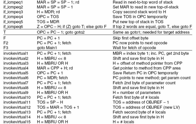
19 TOS and OPC are extra registers. Their use is described below. At the beginning and end of each instruction, TOS contains the value of the memory location pointed to by SP, i.e. the top word on the stack. This value is redundant since it can always be read from memory, but having it in a register often saves a memory reference. The OPC register is a temporary (i.e., scratch) register. It has no preassigned use. It is used, for example, to save the address of the opcode for a branch instruction while PC is incremented to access parameters (e.g. function call). It is also used as a temporary register in the IJVM conditional branch instructions. Like all interpreters, the microprogram of Fig. 9 has a main loop that fetches, decodes, and executes instructions from the program being interpreted, in this case, IJVM instructions. Its main loop begins on the line labeled Main1. It starts with the invariant that PC has previously been loaded with an address of a memory location containing an opcode. Furthermore, that opcode has already been fetched into MBR. Note this implies that when we get back to this line of main loop, we must ensure that PC has been updated to point to the next opcode to be interpreted and the opcode byte itself has already been fetched into MBR. This initial microinstruction sequence is executed at the beginning of every IJVM instruction, so it is important that it be as short as possible. Through careful design of the Mic-1 hardware and software, we have managed to reduce the main loop to a single microinstruction. As stated above, every time this microinstruction is executed, the IJVM opcode to execute is already present in MBR. What the microninstruction does is branch to the beginning of a sequence of microinstructions (in control store) for executing this IJVM instruction and also begin fetching the byte following the IJVM opcode, which may be either an operand byte or the next opcode. To do this branching efficiently, all control store addresses corresponding to IJVM opcodes are reserved for the first microinstruction of the corresponding sequence. This implies that the microinstructions other than the initial one in each sequence must be stuffed away in the holes between reserved addresses. This explains why each microinstruction explicitly names its succeeding microinstruction, instead of having them be located (in control store) and executed sequentially. Conclusively, each sequence starts at the address corresponding to the numerical value of the IJVM opcode it interprets (e.g. IADD starts at 0x60, see Fig. 7), but the rest of the sequence can be anywhere in the control store, and not necessarily at consecutive addresses. Chapter 4 Page 19
20 To see how the micoprogram works, let us assume, for example, that MBR contains the value 0x60, that is, the opcode for IADD. In the one-microinstruction main loop we accomplish three things: 1. Increment the PC, leaving it containing the address of the first byte (in memory) after the opcode. 2. Initiate a fetch of this next byte into MBR. This byte will always be needed sooner or later, either as an operand for the current IJVM instruction or as the next opcode (as in the case of the IADD instruction, which has no operand bytes), so starting the fetch now cannot do any harm in any case. 3. Perform a multiway branch to the address contained in MBR. This address is equal to the numerical value of the opcode currently being executed. It was placed there by the previous microinstruction. Note carefully that the value being fetched in this microinstruction does not play any role in the multiway branch. Since the fetch of the next byte is started in the current data path cycle (for the current microinstruction) and it will only be available by the start of the third microinstruction following (see P.16, the last point of the previous section). The microinstruction branched to by the main loop is the one labeled iadd1 (see Fig 9). This instruction starts the work specific to IADD: (pop two words from stack & push their sum, see. Fig. 7) 1. The TOS is already present, but the next-to-top word of the stack must be fetched from memory. 2. The TOS must be added to the next-to-top word fetched from memory. 3. The result, which is to be pushed on the stack, must be stored back into memory, as well as stored in the TOS. In order to fetch the operand from the memory, it is necessary to decrement the SP and write it into MAR. Note that, conveniently, this address is also the address that will be used for the subsequent write. Furthermore, since this location will be the new top of stack, SP should be assigned this value. Therefore, a single operation can determine the new value of SP and MAR, decrement SP, and write it into both registers. These things are accomplished in the first cycle, iadd1, and the memory read operation is initiated. Chapter 4 Page 20
21 In addition, MPC gets the value from iadd1 s NEXT_ADDRESS field, which is the address of iadd2, wherever it may be. Then iadd2 is read from the control store. During the second cycle, while waiting for the operand to be read in from memory, we copy the top word of the stack from TOS into H, where it will be available for the addition when the read completes. At the beginning of the third cycle, iadd3, MDR contains the addend fetched from memory. In this cycle, it is added to the contents of H, and the result is stored back to MDR, as well as back into TOS. A write operation is also initiated, storing the new top-of-stack word back into memory. In this cycle the goto has the effect of assigning the address of Main1 to MPC, returning us to the starting point for the execution of the next IJVM instruction, now contained in MBR already. Compiling Java to IJVM Let us now see how Java and IJVM relate to one another. In Fig. 10(a) we show a simple fragment of Java code. When fed to a Java compiler, the compiler would probably produce the IJVM assembly language shown in Fig. 10(b). The Java assembler would then translate the assembly program into the binary program shown in Fig. 10(c). For this example, we have assumed that i is the local variable 1, j is local variable 2, and k is local variable 3. Fig. 10. (a) A Java fragment. (b) The corresponding Java assembly language. (c) The IJVM program in hexadecimal. Chapter 4 Page 21
22 The compiled code is straightforward. First j and k are pushed onto the stack, added, and the result stored in i. Then i and the constant 3 are pushed onto the stack and compared. If they are equal, a branch is taken to L1, where k is set to 0. If they are unequal, the compare fails and code following IF_ICMPEQ is executed. When it is done, it branches to L2, where the then and else parts merge. The operand stack for the IJVM program of Fig. 10(b) is shown in Fig. 11. Assuming before the code starts executing, the stack is empty, indicated by the horizontal line above the 0. Fig. 11. The stack after each IJVM instruction of Fig. 10(b), with the corresponding line number indicated at the bottom. Chapter 4 Page 22
23 Chapter 4 Micro-architecture Level PART II Speed versus Cost Reducing the Execution Path Length Merging the Interpreter Loop with the Microcode A Three-Bus Architecture An Instruction Fetch Unit Example JAM = 000 MPC = NEXT_ADDRESS JAM = 001 or 010 MPC = NEXT_ADDRESS with the high-order bit ORed with 1. Address Addr JAM Data path control bits 0*45 0* *46 0* *47 0* *48 0*49 0*50 0*51 0* *52 0*53 0*54 0* *55 0*56 0*57 0*58 Direct Mapped Cache Explain the operating principle of the Direct Mapped Cache. 1. The Valid bit show the valid data is entry or not. When the System is started, the entries will be invalid. 2. The Tag Field consists of the unique, 16 bits values is identifying the corresponding line of the memory from which data is came. Chapter 4 Page 23
24 3. Data Field is contains copy data in the memory, 32 bytes one cache line will holds. For Shorting And Retrieving data from the cache, the address is broken into four components. 1. The Tag Field corresponds to the Tag Bits stored in a cache entry 2. The Line field indicates which cache entry holds the corresponding data. 3. The word field tell which word within a line is referenced 4. The Byte field, if the only one byte is requested, it tells which byte within the word is needed. But it usually not used. Merging the Interpreter Loop wth the Microcode Example: The main loop consists of one microinstruction that must be executed at the beginning of very IJVM instruction. Label Operations Comments pop1 MAR=SP=SP-1; rd Read in next-to-top word on stack pop2 Wait for new TOS to be read from memory Pop3 TOS=MDR; goto Main1 Copy new word to TOS Main1 PC=PC+1; fetch; goto(mbr) MBER holds opcode; Chapter 4 Page 24
25 The dynamic sequence of instructions is shown for a POP instruction.the main loop occurs before and after every instruction; in the table that show only the occurrence after the POP instruction. Notice that the execution of this instruction takes four clock cycles: three for the specific microinstruction for POP and one for the main loop. Label Operations Comments Pop1 MAR=SP=SP-1; rd Read in next-to-top word on stack Main1.pop PC=PC+1; fetch MBR holds opcodes; fetch next byte Pop3 TOS=MDR; goto(mbr) Copy new word to TOS; dispatch on opcode The sequence has been reduced to three instructions by merging the main loop instruction, taking advantage of a clock cycle when the ALU is not used in pop2 to save a cycle and again in Main1. Notice that the end of this sequence branches directly to the specific code for the subsequent instruction, so only three cycles are required total. This little trick reduces the subsequent IADD goes from four cycles to three. It is equivalent to speeding up the clock from 250MHz(4 nses microinstructions) to 33MHz(3 nses microinstruction) for free. The POP instruction is particularly well suited for this treatment, because it has a dead cycle in the middle that does not use the ALU. Thus to reduce the instruction lengthy by one within an instruction requires finding a vycle in the instruction where the ALU is not in use. The first technique for reducing path length: *Merge the interpreter loop into the end of each microcode sequence. Chapter 4 Page 25
26 Three-bus architecture Two bus design only have A bus and B bus, All of the registers should have access to both input buses. Let s consider on the Mic-1 implementation of ILOAD, Mic-1 code for executing ILOAD Label Operations Comments iload1 iload2 iload3 iload4 iload5 Main1 H=LV MAR=MBRU+H;rd MAR=SP=SP+1 PC=PC+1;fetch;wr TOS=MDR;goto Main1 PC=PC+1;fetch;goto(MBR) MBR contain index;copy LV to H MAR=address of local variable to push SP points to nex top of stack;prepare write Inc PC;get next opcode;write top of stack Update TOS MBR holds opcode;get next byte;dispatch We can see here that in iload1, LV is copied into H. The only reason it is copied into H is so it can be added to MBRU in iload2. In the original two-bus design, there is no way to add two arbitrary register, So one of them first has to be copied to H first. But how to improve the performance of a CPU? Let take a look on the Three-bus design. Go from a two bus design to a three bus design. A Three-bus design contail A bus, B bus and C bus, let s consider on the three-bus design for executing ILOAD. Chapter 4 Page 26
27 Three-bus code for executing ILOAD Label Operations Comments iload1 iload2 iload3 iload4 iload5 MAR=MBRU+LV;rd MAR=SP=SP+1 PC=PC+1;fetch;wr TOS=MDR PC=PC+1;fetch;goto(MBR) MAR=address of local variable to push SP points to new top of stack;prepare write Inc PC;get next opcode;write top of stack Update TOS MBR already holds opcode;fetch index byte With our new three-bus design, We can have our second technique for reducing path length, We can save a cycle, we have added the interpreter loop to ILOAD here, but doing so neither increases nor decrease the execution path length. Still. The additional bus has reduced the total execution time of ILOAD from six cycles to five cycles, so a Three-bus architecture can improve the performance of a CPU. An Instruction Fetch Unit Notice that every instruction the following operation may occur: 1. The PC is passed thought the ALU and increment. 2. The PC is used to fetch the next byte in the instruction steam. 3. Operands are read from memory. 4. Operands are written to memory. 5. The ALU does a computation and the result are store back. Much of the load can be remove from the ALU by creating an independent unit to fetch and process the instructions. The unit, called an Instruction Fetch Unit (IFU), can independent increment PC and fetch bytes from the byte stream before they are needed. The unit requires only an increment, a circuit far simpler Chapter 4 Page 27
28 than a full adder. Carrying this idea further, the IFU can also assemble 8- and 16-bit operands so that they are ready for immediate use whenever needed. There are at least two ways this can be accomplished: 1. The IFU can actually interpret each opcode, determining how many additional fields must be fetch, and assemble them into a register ready for use by the main execution unit. 2. The IFU can take advantage of the stream nature of the instructions, and make available at all times the next 8- and 16- bit piece whether or not doing so makes any sense. The main execution unit can then ask for whatever it needs. We show the rudiment of the scheme in Figure 1. Rather than a single 8-bit MBR, there are now two MBRs: the 8-bit MBR1 and the 16-bit MBR2. Fig. 1 The IFU is responsible for fetching a stream of bytes. It does this by using a conventional 4-byte memory port, fetching entire 4-byte words ahead of time and loading the consecutive bytes into supplies them one or two at a time, in the order to fetched. The design of the IFU can be read modeled by an FSM (Finite State Machine) as shown. All FSMs consist of two parts : states, shown as circles, and transitions, shown as arcs from one state to Chapter 4 Page 28
29 another. Each state represents one possible situation the FSM can be in. This particular FSM has seven states, corresponding to the seven states of the shift register of Fig 2. The seven states correspond to how many bytes are currently in the shift register, a number between 0 and 6, inclusive. Fig. 2 The IFU has its own memory address register, called IMAR, which is used to address memory when a new word has to be fetched. This register has its own dedicated incrementer so that the main ALU is not needed to increment it to get the next word. Pipelining There are three major components to the actual data path cycle: 1. The time to drive the selected registers onto the A bus and B bus. 2. The time for the ALU and shifter to do their work. 3. The time for the results to get back to the registers and be stored. Since it takes three clock cycles to use the data path, then we insert 3 latches onto A bus, B bus and C bus, they can help us to speed up the clock by shorter the maximum delay and use all parts of the data path during every cycle. Now all the operations required 3 cycles to operate, we will explain it in the following example: Chapter 4 Page 29
30 Label Operations Comments Swap1 MAR = SP 1; rd Read 2 nd word from stack; set MAR to Swap2 MAR = SP Prepare to write new 2 nd word Swap3 H = MDA; wr Save new TOS; write 2 nd word to SP stack Swap4 MDR = TOS Copy old TOS to MDR Swap5 MAR = SP 1; wr Write old TOS to 2 nd place on stack Swap6 TOS = H; goto (MBR1) Update TOS Figure 3. The Mic-2 code for SWAP. Each operations is divided into many pieces, called microstep. In Fig 3, the operations of swap1 is MAR = SP 1; rd, but it can divide into 4 microsteps: 1. Copying SP to B 2. Subtract 1 from B and send to C 3. The result is stored in MAR and read it 4. Memory reads and assign to MDR Each swap can divide into some microsteps. From the microsteps, we can do pipelining to improve the speed. The Cy(cycle) in the Mic-2 is equal to 3 cycle in Mic-3, so it can improve the speed. Before explain Fig 4, we want to talk something about true dependence, it is a rule of pipelining. It means a microstep cannot start until the previous microstep produce result. In Fig 4, we see that swap1 is divided into 4 microsteps, and it total used 4 cycles. But swap2 start in cycle 2 to do its first microstep, since swap1 used B in cycle 1 and cycle 2, swap2 can use B in the situation that do not affect swap1, then it start in cycle 2. Base on this reason, we can explain the following cycles. Chapter 4 Page 30
31 There is something special in swap3, it can only start its first microstep in cycle 5, since the first microstep is run MDR through the ALU, and MDR will not available from memory until the start of cycle 5. So it can only start at cycle 5. Swap1 Swap2 Swap3 Swap4 Swap5 Swap6 Cy MAR=SP 1; rd MAR = SP H=MDR;wr MDR=TOS MAR=SP-1;wr TOS=H;goto (MBR1) 1 B=SP 2 C=B-1 B=SP 3 MAR=C; rd C=B 4 MDR=mem MAR=C 5 B=MDR 6 C=B B=TOS 7 H=C; wr C=B B=SP 8 Mem=MDR MDR=C C=B-1 B=H 9 MAR=C; wr C=B 10 Mem=MDR TOS=C 11 Goto (MBR1) Figure 4. The implementation of SWAP on the Mic-3. Chapter 4 Page 31
CS Computer Architecture
 CS 35101 Computer Architecture Section 600 Dr. Angela Guercio Fall 2010 An Example Implementation In principle, we could describe the control store in binary, 36 bits per word. We will use a simple symbolic
The Microarchitecture Level
 The Microarchitecture Level Chapter 4 The Data Path (1) The data path of the example microarchitecture used in this chapter. The Data Path (2) Useful combinations of ALU signals and the function performed.
Topics. Block Diagram of Mic-1 Microarchitecture. Review Sheet. Microarchitecture IJVM ISA
 Topics Review Sheet Microarchitecture IJVM ISA 1 Block Diagram of Mic-1 Microarchitecture Datapath Part of CPU containing ALU, its inputs, and its outputs Purpose Implement the ISA level above it (macroarchitecture)
Topics. Computer Organization CS Mic-1 Microinstructions. Control Store (ROM) Programming Teams
 Programming Teams") Computer Organization CS -0 Mic- Microinstructions Dr. William H. Robinson November, 004 http://eecs.vanderbilt.edu/courses/cs/ Topics There is no one giant step that does it. It's a lot of little steps.
Computer Organization CS -0 Mic- Microinstructions Dr. William H. Robinson November, 004 http://eecs.vanderbilt.edu/courses/cs/ Topics There is no one giant step that does it. It's a lot of little steps.
Topics. Computer Organization CS Exam 2 Review. Infix Notation. Reverse Polish Notation (RPN)
") Computer Organization CS 231-01 Exam 2 Review Dr. William H. Robinson October 11, 2004 http://eecs.vanderbilt.edu/courses/cs231/ Topics Education is a progressive discovery of our own ignorance. Will Durant
Computer Organization CS 231-01 Exam 2 Review Dr. William H. Robinson October 11, 2004 http://eecs.vanderbilt.edu/courses/cs231/ Topics Education is a progressive discovery of our own ignorance. Will Durant
Digital System Design Using Verilog. - Processing Unit Design
 Digital System Design Using Verilog - Processing Unit Design 1.1 CPU BASICS A typical CPU has three major components: (1) Register set, (2) Arithmetic logic unit (ALU), and (3) Control unit (CU) The register
Module 5 - CPU Design
 Module 5 - CPU Design Lecture 1 - Introduction to CPU The operation or task that must perform by CPU is: Fetch Instruction: The CPU reads an instruction from memory. Interpret Instruction: The instruction
Computer Science 324 Computer Architecture Mount Holyoke College Fall Topic Notes: Data Paths and Microprogramming
 Computer Science 324 Computer Architecture Mount Holyoke College Fall 2007 Topic Notes: Data Paths and Microprogramming We have spent time looking at the MIPS instruction set architecture and building
4. MICROPROGRAMMED COMPUTERS
 Structure of Computer Systems Laboratory No. 4 1 4. MICROPROGRAMMED COMPUTERS This laboratory work presents the principle of microprogrammed computers and an example of microprogrammed architecture, in
Basic Processing Unit: Some Fundamental Concepts, Execution of a. Complete Instruction, Multiple Bus Organization, Hard-wired Control,
 UNIT - 7 Basic Processing Unit: Some Fundamental Concepts, Execution of a Complete Instruction, Multiple Bus Organization, Hard-wired Control, Microprogrammed Control Page 178 UNIT - 7 BASIC PROCESSING
Where Does The Cpu Store The Address Of The
 Where Does The Cpu Store The Address Of The Next Instruction To Be Fetched The three most important buses are the address, the data, and the control buses. The CPU always knows where to find the next instruction
5.7. Microprogramming: Simplifying Control Design 5.7
 5.7 Microprogramming: Simplifying Control Design 5.7 For the of our simple MIPS subset, a graphical representation of the finite state machine, as in Figure 5.40 on page 345, is certainly adequate. We
1DT157 Digitalteknik och datorarkitekt. Digital technology and computer architecture, 5p
 1DT157 Digitalteknik och datorarkitekt Digital technology and computer architecture, 5p Homework #1 Tanenbaum Chapter 3 Problems 6,7,11,19,23 Submit electronically to the TAs: Binary Numbers Appendix A
EE 3170 Microcontroller Applications
 EE 3170 Microcontroller Applications Lecture 4 : Processors, Computers, and Controllers - 1.2 (reading assignment), 1.3-1.5 Based on slides for ECE3170 by Profs. Kieckhafer, Davis, Tan, and Cischke Outline
Processing Unit CS206T
 Processing Unit CS206T Microprocessors The density of elements on processor chips continued to rise More and more elements were placed on each chip so that fewer and fewer chips were needed to construct
 Chapter 1 Microprocessor architecture ECE 3120 Dr. Mohamed Mahmoud http://iweb.tntech.edu/mmahmoud/ mmahmoud@tntech.edu Outline 1.1 Computer hardware organization 1.1.1 Number System 1.1.2 Computer hardware
COMPUTER ARCHITECTURE AND ORGANIZATION Register Transfer and Micro-operations 1. Introduction A digital system is an interconnection of digital
 Register Transfer and Micro-operations 1. Introduction A digital system is an interconnection of digital hardware modules that accomplish a specific information-processing task. Digital systems vary in
Topic #6. Processor Design
 Topic #6 Processor Design Major Goals! To present the single-cycle implementation and to develop the student's understanding of combinational and clocked sequential circuits and the relationship between
ASSEMBLY LANGUAGE MACHINE ORGANIZATION
 ASSEMBLY LANGUAGE MACHINE ORGANIZATION CHAPTER 3 1 Sub-topics The topic will cover: Microprocessor architecture CPU processing methods Pipelining Superscalar RISC Multiprocessing Instruction Cycle Instruction
Microcontroller Systems
 µcontroller systems 1 / 43 Microcontroller Systems Engineering Science 2nd year A2 Lectures Prof David Murray david.murray@eng.ox.ac.uk www.robots.ox.ac.uk/ dwm/courses/2co Michaelmas 2014 µcontroller
MICROPROGRAMMED CONTROL
 MICROPROGRAMMED CONTROL Hardwired Control Unit: When the control signals are generated by hardware using conventional logic design techniques, the control unit is said to be hardwired. Micro programmed
Advanced Parallel Architecture Lesson 3. Annalisa Massini /2015
 Advanced Parallel Architecture Lesson 3 Annalisa Massini - 2014/2015 Von Neumann Architecture 2 Summary of the traditional computer architecture: Von Neumann architecture http://williamstallings.com/coa/coa7e.html
Computer Architecture Programming the Basic Computer
 4. The Execution of the EXCHANGE Instruction The EXCHANGE routine reads the operand from the effective address and places it in DR. The contents of DR and AC are interchanged in the third microinstruction.
MARIE: An Introduction to a Simple Computer
 MARIE: An Introduction to a Simple Computer 4.2 CPU Basics The computer s CPU fetches, decodes, and executes program instructions. The two principal parts of the CPU are the datapath and the control unit.
Chapter 16. Control Unit Operation. Yonsei University
 Chapter 16 Control Unit Operation Contents Micro-Operation Control of the Processor Hardwired Implementation 16-2 Micro-Operations Micro-Operations Micro refers to the fact that each step is very simple
Lecture1: introduction. Outline: History overview Central processing unite Register set Special purpose address registers Datapath Control unit
 Lecture1: introduction Outline: History overview Central processing unite Register set Special purpose address registers Datapath Control unit 1 1. History overview Computer systems have conventionally
Chapter 3 : Control Unit
 3.1 Control Memory Chapter 3 Control Unit The function of the control unit in a digital computer is to initiate sequences of microoperations. When the control signals are generated by hardware using conventional
Computer Architecture
 Computer Architecture Lecture 1: Digital logic circuits The digital computer is a digital system that performs various computational tasks. Digital computers use the binary number system, which has two
UNIT-II. Part-2: CENTRAL PROCESSING UNIT
 Page1 UNIT-II Part-2: CENTRAL PROCESSING UNIT Stack Organization Instruction Formats Addressing Modes Data Transfer And Manipulation Program Control Reduced Instruction Set Computer (RISC) Introduction:
Chapter 12. CPU Structure and Function. Yonsei University
 Chapter 12 CPU Structure and Function Contents Processor organization Register organization Instruction cycle Instruction pipelining The Pentium processor The PowerPC processor 12-2 CPU Structures Processor
Chapter 4. MARIE: An Introduction to a Simple Computer
 Chapter 4 MARIE: An Introduction to a Simple Computer Chapter 4 Objectives Learn the components common to every modern computer system. Be able to explain how each component contributes to program execution.
Major and Minor States
 Major and Minor States We now consider the micro operations and control signals associated with the execution of each instruction in the ISA. The execution of each instruction is divided into three phases.
CS 31: Intro to Systems Digital Logic. Kevin Webb Swarthmore College February 2, 2016
 CS 31: Intro to Systems Digital Logic Kevin Webb Swarthmore College February 2, 2016 Reading Quiz Today Hardware basics Machine memory models Digital signals Logic gates Circuits: Borrow some paper if
CPU Structure and Function
 Computer Architecture Computer Architecture Prof. Dr. Nizamettin AYDIN naydin@yildiz.edu.tr nizamettinaydin@gmail.com http://www.yildiz.edu.tr/~naydin CPU Structure and Function 1 2 CPU Structure Registers
Blog - https://anilkumarprathipati.wordpress.com/
 Control Memory 1. Introduction The function of the control unit in a digital computer is to initiate sequences of microoperations. When the control signals are generated by hardware using conventional
CS Computer Architecture
 CS 35101 Computer Architecture Section 600 Dr. Angela Guercio Fall 2010 Computer Systems Organization The CPU (Central Processing Unit) is the brain of the computer. Fetches instructions from main memory.
Mapping Control to Hardware
 C A P P E N D I X A custom format such as this is slave to the architecture of the hardware and the instruction set it serves. The format must strike a proper compromise between ROM size, ROM-output decoding,
Class Notes. Dr.C.N.Zhang. Department of Computer Science. University of Regina. Regina, SK, Canada, S4S 0A2
 Class Notes CS400 Part VI Dr.C.N.Zhang Department of Computer Science University of Regina Regina, SK, Canada, S4S 0A2 C. N. Zhang, CS400 83 VI. CENTRAL PROCESSING UNIT 1 Set 1.1 Addressing Modes and Formats
Computer Science 324 Computer Architecture Mount Holyoke College Fall Topic Notes: MIPS Instruction Set Architecture
 Computer Science 324 Computer Architecture Mount Holyoke College Fall 2009 Topic Notes: MIPS Instruction Set Architecture vonneumann Architecture Modern computers use the vonneumann architecture. Idea:
CS 31: Intro to Systems Digital Logic. Kevin Webb Swarthmore College February 3, 2015
 CS 31: Intro to Systems Digital Logic Kevin Webb Swarthmore College February 3, 2015 Reading Quiz Today Hardware basics Machine memory models Digital signals Logic gates Circuits: Borrow some paper if
The CPU and Memory. How does a computer work? How does a computer interact with data? How are instructions performed? Recall schematic diagram:
 The CPU and Memory How does a computer work? How does a computer interact with data? How are instructions performed? Recall schematic diagram: 1 Registers A register is a permanent storage location within
Topics. Structured Computer Organization. Assembly language. IJVM instruction set. Mic-1 simulator programming
 Topics Assembly language IJVM instruction set Mic-1 simulator programming http://www.ontko.com/mic1/ Available in 2 nd floor PC lab S/W found in directory C:\mic1 1 Structured Computer Organization 2 Block
Chapter 4. MARIE: An Introduction to a Simple Computer 4.8 MARIE 4.8 MARIE A Discussion on Decoding
 4.8 MARIE This is the MARIE architecture shown graphically. Chapter 4 MARIE: An Introduction to a Simple Computer 2 4.8 MARIE MARIE s Full Instruction Set A computer s control unit keeps things synchronized,
Chapter 17. Microprogrammed Control. Yonsei University
 Chapter 17 Microprogrammed Control Contents Basic Concepts Microinstruction Sequencing Microinstruction Execution TI 8800 Applications of Microprogramming 17-2 Introduction Basic Concepts An alternative
Materials: 1. Projectable Version of Diagrams 2. MIPS Simulation 3. Code for Lab 5 - part 1 to demonstrate using microprogramming
 CS311 Lecture: CPU Control: Hardwired control and Microprogrammed Control Last revised October 18, 2007 Objectives: 1. To explain the concept of a control word 2. To show how control words can be generated
(Refer Slide Time: 1:40)
") Computer Architecture Prof. Anshul Kumar Department of Computer Science and Engineering, Indian Institute of Technology, Delhi Lecture - 3 Instruction Set Architecture - 1 Today I will start discussion
Computer Architecture Prof. Anshul Kumar Department of Computer Science and Engineering, Indian Institute of Technology, Delhi Lecture - 3 Instruction Set Architecture - 1 Today I will start discussion
STRUCTURE OF DESKTOP COMPUTERS
 Page no: 1 UNIT 1 STRUCTURE OF DESKTOP COMPUTERS The desktop computers are the computers which are usually found on a home or office desk. They consist of processing unit, storage unit, visual display
Topic Notes: MIPS Instruction Set Architecture
 Computer Science 220 Assembly Language & Comp. Architecture Siena College Fall 2011 Topic Notes: MIPS Instruction Set Architecture vonneumann Architecture Modern computers use the vonneumann architecture.
MARIE: An Introduction to a Simple Computer
 MARIE: An Introduction to a Simple Computer Outline Learn the components common to every modern computer system. Be able to explain how each component contributes to program execution. Understand a simple
CPU. Fall 2003 CSE 207 Digital Design Project #4 R0 R1 R2 R3 R4 R5 R6 R7 PC STATUS IR. Control Logic RAM MAR MDR. Internal Processor Bus
 http://www.engr.uconn.edu/~barry/cse207/fa03/project4.pdf Page 1 of 16 Fall 2003 CSE 207 Digital Design Project #4 Background Microprocessors are increasingly common in every day devices. Desktop computers
Chapter 4. MARIE: An Introduction to a Simple Computer. Chapter 4 Objectives. 4.1 Introduction. 4.2 CPU Basics
 Chapter 4 Objectives Learn the components common to every modern computer system. Chapter 4 MARIE: An Introduction to a Simple Computer Be able to explain how each component contributes to program execution.
Multicycle conclusion
 Multicycle conclusion The last few lectures covered a lot of material! We introduced a multicycle datapath, where different instructions take different numbers of cycles to execute. A multicycle unit is
DC57 COMPUTER ORGANIZATION JUNE 2013
 Q2 (a) How do various factors like Hardware design, Instruction set, Compiler related to the performance of a computer? The most important measure of a computer is how quickly it can execute programs.
A3 Computer Architecture
 A3 Computer Architecture Engineering Science 3rd year A3 Lectures Prof David Murray david.murray@eng.ox.ac.uk www.robots.ox.ac.uk/ dwm/courses/3co Michaelmas 2000 1 / 1 2: Introduction to the CPU 3A3 Michaelmas
Page 521 CPSC 5155 Last Revised July 9, 2011 Copyright 2011 by Edward L. Bosworth, Ph.D. All rights reserved.
 Chapter 15 Implementation of the Central Processing Unit In this chapter, we continue consideration of the design and implementation of the CPU, more specifically the control unit of the CPU. In previous
1. Internal Architecture of 8085 Microprocessor
 1. Internal Architecture of 8085 Microprocessor Control Unit Generates signals within up to carry out the instruction, which has been decoded. In reality causes certain connections between blocks of the
CS2214 COMPUTER ARCHITECTURE & ORGANIZATION SPRING 2014
 CS2214 COMPUTER ARCHITECTURE & ORGANIZATION SPRING 2014 DIGITAL SYSTEM DESIGN BASICS 1. Introduction A digital system performs microoperations. The most well known digital system example is is a microprocessor.
Lecture-15 W-Z: Increment-Decrement Address Latch:
 Lecture-15 W-Z: (W) and (Z) are two 8-bit temporary registers not accessible to the user. They are exclusively used for the internal operation by the microprocessor. These registers are used either to
PROBLEMS. 7.1 Why is the Wait-for-Memory-Function-Completed step needed when reading from or writing to the main memory?
 446 CHAPTER 7 BASIC PROCESSING UNIT (Corrisponde al cap. 10 - Struttura del processore) PROBLEMS 7.1 Why is the Wait-for-Memory-Function-Completed step needed when reading from or writing to the main memory?
Machine Language Instructions Introduction. Instructions Words of a language understood by machine. Instruction set Vocabulary of the machine
 Machine Language Instructions Introduction Instructions Words of a language understood by machine Instruction set Vocabulary of the machine Current goal: to relate a high level language to instruction
Computer Systems. Binary Representation. Binary Representation. Logical Computation: Boolean Algebra
 Binary Representation Computer Systems Information is represented as a sequence of binary digits: Bits What the actual bits represent depends on the context: Seminar 3 Numerical value (integer, floating
Introduction to Computers - Chapter 4
 Introduction to Computers - Chapter 4 Since the invention of the transistor and the first digital computer of the 1940s, computers have been increasing in complexity and performance; however, their overall
COMPUTER ORGANIZATION & ARCHITECTURE
 COMPUTER ORGANIZATION & ARCHITECTURE Instructions Sets Architecture Lesson 5a 1 What are Instruction Sets The complete collection of instructions that are understood by a CPU Can be considered as a functional
Materials: 1. Projectable Version of Diagrams 2. MIPS Simulation 3. Code for Lab 5 - part 1 to demonstrate using microprogramming
 CPS311 Lecture: CPU Control: Hardwired control and Microprogrammed Control Last revised October 23, 2015 Objectives: 1. To explain the concept of a control word 2. To show how control words can be generated
Instructions: Assembly Language
 Chapter 2 Instructions: Assembly Language Reading: The corresponding chapter in the 2nd edition is Chapter 3, in the 3rd edition it is Chapter 2 and Appendix A and in the 4th edition it is Chapter 2 and
Chapter 14 Design of the Central Processing Unit
 Chapter 14 Design of the Central Processing Unit We now focus on the detailed design of the CPU (Central Processing Unit) of the Boz 7. The CPU has two major components: the Control Unit and the ALU (Arithmetic
Lecture #2 January 30, 2004 The 6502 Architecture
 Lecture #2 January 30, 2004 The 6502 Architecture In order to understand the more modern computer architectures, it is helpful to examine an older but quite successful processor architecture, the MOS-6502.
CPU Design John D. Carpinelli, All Rights Reserved 1
 CPU Design 1997 John D. Carpinelli, All Rights Reserved 1 Outline Register organization ALU design Stacks Instruction formats and types Addressing modes 1997 John D. Carpinelli, All Rights Reserved 2 We
1. INTRODUCTION TO MICROPROCESSOR AND MICROCOMPUTER ARCHITECTURE:
 1. INTRODUCTION TO MICROPROCESSOR AND MICROCOMPUTER ARCHITECTURE: A microprocessor is a programmable electronics chip that has computing and decision making capabilities similar to central processing unit
Introduction to CPU Design
 ١ Introduction to CPU Design Computer Organization & Assembly Language Programming Dr Adnan Gutub aagutub at uqu.edu.sa [Adapted from slides of Dr. Kip Irvine: Assembly Language for Intel-Based Computers]
Programmable machines
 Page 1 of 9 Programmable machines indicates problems that have been selected for discussion in section, time permitting. Problem 1. Consider the following circuit: The heavy lines represent busses, which
COSC 243. Computer Architecture 1. COSC 243 (Computer Architecture) Lecture 6 - Computer Architecture 1 1
 Lecture 6 - Computer Architecture 1 1") COSC 243 Computer Architecture 1 COSC 243 (Computer Architecture) Lecture 6 - Computer Architecture 1 1 Overview Last Lecture Flip flops This Lecture Computers Next Lecture Instruction sets and addressing
COSC 243 Computer Architecture 1 COSC 243 (Computer Architecture) Lecture 6 - Computer Architecture 1 1 Overview Last Lecture Flip flops This Lecture Computers Next Lecture Instruction sets and addressing
CPE 323 MSP430 INSTRUCTION SET ARCHITECTURE (ISA)
") CPE 323 MSP430 INSTRUCTION SET ARCHITECTURE (ISA) Aleksandar Milenković Email: milenka@uah.edu Web: http://www.ece.uah.edu/~milenka Objective Introduce MSP430 Instruction Set Architecture (Class of ISA,
CPE 323 MSP430 INSTRUCTION SET ARCHITECTURE (ISA) Aleksandar Milenković Email: milenka@uah.edu Web: http://www.ece.uah.edu/~milenka Objective Introduce MSP430 Instruction Set Architecture (Class of ISA,
PESIT Bangalore South Campus
 INTERNAL ASSESSMENT TEST I Date: 30/08/2017 Max Marks: 40 Subject & Code: Computer Organization 15CS34 Semester: III (A & B) Name of the faculty: Mrs.Sharmila Banu.A Time: 8.30 am 10.00 am Answer any FIVE
Micro-programmed Control Ch 15
 Micro-programmed Control Ch 15 Micro-instructions Micro-programmed Control Unit Sequencing Execution Characteristics 1 Hardwired Control (4) Complex Fast Difficult to design Difficult to modify Lots of
Chapter 4. The Processor
 Chapter 4 The Processor Introduction CPU performance factors Instruction count Determined by ISA and compiler CPI and Cycle time Determined by CPU hardware We will examine two MIPS implementations A simplified
Advanced Parallel Architecture Lesson 3. Annalisa Massini /2015
 Advanced Parallel Architecture Lesson 3 Annalisa Massini - Von Neumann Architecture 2 Two lessons Summary of the traditional computer architecture Von Neumann architecture http://williamstallings.com/coa/coa7e.html
MICROPROCESSOR AND MICROCONTROLLER BASED SYSTEMS
 MICROPROCESSOR AND MICROCONTROLLER BASED SYSTEMS UNIT I INTRODUCTION TO 8085 8085 Microprocessor - Architecture and its operation, Concept of instruction execution and timing diagrams, fundamentals of
Machine Instructions vs. Micro-instructions. Micro-programmed Control Ch 15. Machine Instructions vs. Micro-instructions (2) Hardwired Control (4)
 Hardwired Control (4)") Micro-programmed Control Ch 15 Micro-instructions Micro-programmed Control Unit Sequencing Execution Characteristics 1 Machine Instructions vs. Micro-instructions Memory execution unit CPU control memory
Micro-programmed Control Ch 15 Micro-instructions Micro-programmed Control Unit Sequencing Execution Characteristics 1 Machine Instructions vs. Micro-instructions Memory execution unit CPU control memory
Design of Decode, Control and Associated Datapath Units
 1 Design of Decode, Control and Associated Datapath Units ECE/CS 3710 - Computer Design Lab Lab 3 - Due Date: Thu Oct 18 I. OVERVIEW In the previous lab, you have designed the ALU and hooked it up with
Micro-programmed Control Ch 15
 Micro-programmed Control Ch 15 Micro-instructions Micro-programmed Control Unit Sequencing Execution Characteristics 1 Hardwired Control (4) Complex Fast Difficult to design Difficult to modify Lots of
CPE300: Digital System Architecture and Design
 CPE300: Digital System Architecture and Design Fall 2011 MW 17:30-18:45 CBC C316 Pipelining 11142011 http://www.egr.unlv.edu/~b1morris/cpe300/ 2 Outline Review I/O Chapter 5 Overview Pipelining Pipelining
 Part A Questions 1. What is an ISP? ISP stands for Instruction Set Processor. This unit is simply called as processor which executes machine instruction and coordinates the activities of other units..
Chapter 4. The Processor
 Chapter 4 The Processor Introduction CPU performance factors Instruction count Determined by ISA and compiler CPI and Cycle time Determined by CPU hardware 4.1 Introduction We will examine two MIPS implementations
Rui Wang, Assistant professor Dept. of Information and Communication Tongji University.
 Instructions: ti Language of the Computer Rui Wang, Assistant professor Dept. of Information and Communication Tongji University it Email: ruiwang@tongji.edu.cn Computer Hierarchy Levels Language understood
Chapter 4. Chapter 4 Objectives. MARIE: An Introduction to a Simple Computer
 Chapter 4 MARIE: An Introduction to a Simple Computer Chapter 4 Objectives Learn the components common to every modern computer system. Be able to explain how each component contributes to program execution.
Chapter 1. Microprocessor architecture ECE Dr. Mohamed Mahmoud.
 Chapter 1 Microprocessor architecture ECE 3130 Dr. Mohamed Mahmoud The slides are copyright protected. It is not permissible to use them without a permission from Dr Mahmoud http://www.cae.tntech.edu/~mmahmoud/
ADVANCED COMPUTER ARCHITECTURE TWO MARKS WITH ANSWERS
 ADVANCED COMPUTER ARCHITECTURE TWO MARKS WITH ANSWERS 1.Define Computer Architecture Computer Architecture Is Defined As The Functional Operation Of The Individual H/W Unit In A Computer System And The
Blog -
 . Instruction Codes Every different processor type has its own design (different registers, buses, microoperations, machine instructions, etc) Modern processor is a very complex device It contains Many
CC 311- Computer Architecture. The Processor - Control
 CC 311- Computer Architecture The Processor - Control Control Unit Functions: Instruction code Control Unit Control Signals Select operations to be performed (ALU, read/write, etc.) Control data flow (multiplexor
8086 INTERNAL ARCHITECTURE
 8086 INTERNAL ARCHITECTURE Segment 2 Intel 8086 Microprocessor The 8086 CPU is divided into two independent functional parts: a) The Bus interface unit (BIU) b) Execution Unit (EU) Dividing the work between
Advanced Computer Architecture
 Advanced Computer Architecture Lecture No. 22 Reading Material Vincent P. Heuring&Harry F. Jordan Chapter 5 Computer Systems Design and Architecture 5.3 Summary Microprogramming Working of a General Microcoded
Microprogrammed Control Approach
 Microprogrammed Control Approach Considering the FSM for our MIPS subset has 10 states, the complete MIPS instruction set, which contains more than 100 instructions, and considering that these instructions
CS 101, Mock Computer Architecture
 CS 101, Mock Computer Architecture Computer organization and architecture refers to the actual hardware used to construct the computer, and the way that the hardware operates both physically and logically
1 MALP ( ) Unit-1. (1) Draw and explain the internal architecture of 8085.
 Unit-1. (1) Draw and explain the internal architecture of 8085.") (1) Draw and explain the internal architecture of 8085. The architecture of 8085 Microprocessor is shown in figure given below. The internal architecture of 8085 includes following section ALU-Arithmetic
(1) Draw and explain the internal architecture of 8085. The architecture of 8085 Microprocessor is shown in figure given below. The internal architecture of 8085 includes following section ALU-Arithmetic
Darshan Institute of Engineering & Technology for Diploma Studies Unit - 1
 Darshan Institute of Engineering & Technology for Diploma Studies Unit - 1 1. Draw and explain 4 bit binary arithmetic or adder circuit diagram. A binary parallel adder is digital function that produces
Micro-programmed Control Ch 17
 Micro-programmed Control Ch 17 Micro-instructions Micro-programmed Control Unit Sequencing Execution Characteristics Course Summary 1 Hardwired Control (4) Complex Fast Difficult to design Difficult to
Register Transfer and Micro-operations
 Register Transfer Language Register Transfer Bus Memory Transfer Micro-operations Some Application of Logic Micro Operations Register Transfer and Micro-operations Learning Objectives After reading this
Hardwired Control (4) Micro-programmed Control Ch 17. Micro-programmed Control (3) Machine Instructions vs. Micro-instructions
 Micro-programmed Control Ch 17. Micro-programmed Control (3) Machine Instructions vs. Micro-instructions") Micro-programmed Control Ch 17 Micro-instructions Micro-programmed Control Unit Sequencing Execution Characteristics Course Summary Hardwired Control (4) Complex Fast Difficult to design Difficult to modify
Micro-programmed Control Ch 17 Micro-instructions Micro-programmed Control Unit Sequencing Execution Characteristics Course Summary Hardwired Control (4) Complex Fast Difficult to design Difficult to modify
Chapter 4. The Processor
 Chapter 4 The Processor Introduction CPU performance factors Instruction count Determined by ISA and compiler CPI and Cycle time Determined by CPU hardware We will examine two MIPS implementations A simplified