EMBEDDED SYSTEM DESIGN (10EC74)
|
|
|
- Patrick Price
- 6 years ago
- Views:
Transcription
1 UNIT 2 The Hardware Side: An Introduction, The Core Level, Representing Information, Understanding Numbers, Addresses, Instructions, Registers-A First Look, Embedded Systems-An Instruction Set View, Embedded Systems-A Register View, Register View of a Microprocessor The Hardware Side: Storage Elements and Finite-State Machines (2 hour) The concepts of State and Time, The State Diagram, Finite State Machines- A Theoretical Model An Introduction As we know the essential elements for an embedded system are hardware, software and firmware and each will bring out strengths and weaknesses of the embedded system. Here we study about the high level structure and components of the embedded systems are hardware and computing core of an embedded application. That core is usually manifest as a microprocessor, microcomputer, and microcontroller. In today s high-tech and changing world, we can put together a working hierarchy of hardware components. At the top, we find VLSI (Very Large-Scale Integrated) circuits comprising significant pieces of functionality: microprocessors, microcontrollers, FPGAs (Field Programmable Gate Arrays), (C)PLDs ((Complex) Programmable Logic Devices), and ASICs (Application Specific Integrated Circuits). Perhaps we could include memories as well. At the next level down, we find MSI (Medium-Scale Integrated) circuits, which bring smaller, yet complete, pieces of functionality. Going down one more step, we have SSI (Small-Scale Integrated) circuits. At the very bottom, we have the electrical signals we use to represent our data and control information and the other signals that come into our system as noise or other unwanted signals. Throughout our studies on the hardware side, we will utilize the Verilog modelling language to enable us to test, confirm, and demonstrate the viability of our designs prior to committing to hardware. The language will enable us to work at various levels of detail at the top or behavioral level, we can confirm high-level functionality, and at the lower level or structural level, we can confirm details of timing, scheduling, and control. Facility at both levels is essential today. Our study of the hardware side of embedded systems begins with a high-level view of the computing core of the system. We will expand and refine that view to include a detailed discussion of the hardware (and its interaction with the software) both inside and outside of that core. Figure 2.1 illustrates the sequence we follow. DEPT OF ECE, AGMRCET VARUR 1

2 The computing core is the central hardware component in any modern embedded application. It often appears as a microprocessor, microcomputer, or microcontroller. Occasionally, it may appear as a custom-designed VLSI circuit or FPGA. It interacts with and utilizes the remaining components of the system to implement the required application. Such actions are under the control of a set of software and firmware instructions. Information and data come into the system from the surrounding environment and from the application. These data are processed according to the software instructions into signals that are sent back out of the system to the application. The software and firmware instructions, as well as signals coming into or going out of the system, are stored in memory. The Core Level A model comprising four major functional blocks (input, output, memory, and datapath and control) depicting the embedded hardware core and the high level signal flow. These are illustrated in Figure 2.2. DEPT OF ECE, AGMRCET VARUR 2


3 Figure 2.2 Four Major blocks of an embedded hardware, the memory block serves to hold collections of program instructions that we call software and firmware as well as to provide short-term storage for input data, output data, and intermediate results of computations. Data as well as other kinds of signals come into the system from the external world through the input block. Once inside of the system, they may be directed to any number of destinations. The output block provides the means to send data or other signals back to the outside world. The datapath and control block, more commonly known as the CPU or central processing unit, coordinates the activities of the system as well as performs computations and data manipulation operations necessary to executing the application. For the execution, the CPU fetches instructions from memory, interprets them, and then performs the task indicated by the instruction. In doing so, it may retrieve additional data from memory or from the input block. Often, it will also produce information that is sent out of the system. We move signals into, out of, or throughout the system on paths called busses. In their most common implementation, busses are simply collections of wires that are carrying related electrical signals from one place to another.. Signals flowing on the wires making up the busses are classified into three major categories: address, data and control. The data are the key signals that are being moved around; The address signals identify where the data is coming from and where it is going to. The control signals specify and coordinate how the data is transported. DEPT OF ECE, AGMRCET VARUR 3


4 The width of a bus, that is, the number of signals or bits that it can carry simultaneously, provides an indirect measure of how quickly information can be moved. Transferring 64 bits of data on a bus that is 32 bits wide requires two transfers to move the data. In contrast, a bus that is only 8 bits wide will require eight transfers. Figure 2.3 illustrates moving such a set of data over an 8-bit bus from a source module to a destination module. In the model, each transfer requires one time unit; the process begins at time t0 and completes at time t7. Time increases to the left. The source of the transfer is the array of eight bit values; the destination is perhaps a display. In Figure 2.4, we refine the high-level functional diagram to illustrate a typical bus configuration comprising the address, data, and control lines. None of the busses is required to have the same number of lines. To avoid cluttering a drawing by including all of the signals or conducting paths that make up a bus, we will often label the bus width using the annotation / bus width as illustrated in Figure 2.5 In this example, the address bus is shown to have 18 signals, the data bus 16, and the control bus 7. DEPT OF ECE, AGMRCET VARUR 4


5 The microprocessor A microprocessor is a device that will receive inputs and process the data and gives the output. It is often simply referred to as a CPU or datapath. Microprocessors differ in complexity, power consumption, and cost. Today microprocessors range from devices with only a few thousand transistors at cost of a dollar or less to units with 5 to 10 million transistors at a cost of several thousand dollars. The figure 2.6 shows the microprocessor based embedded system, it clearly shows that the microprocessor solely cannot act as an embedded system because it needs a support from other peripherals so different blocks such as ROM memory to store the firmware, RAM memory to store the data, Real Time Clock to strictly follow the time constraints and input and output peripherals. DEPT OF ECE, AGMRCET VARUR 5


6 The microcomputer The microcomputer is a complete computer system that uses a microprocessor as a CPU, typically a microcomputer will also utilize numerous other large scale integrated circuits to provide necessary functionality. The complexity of the microcomputer varies from simple units tha ate implemented on a chip along with the small amount of on-chip memory and elementary I/O system to the complex that will have a microprocessor with a wide array of powerful peripheral circuitry. The Microcontroller The block diagram of the microcontroller based embedded system is shown in figure 2.7 below. Basically microcontroller it receives the input from the external world and does some process on the data and the output of the microcontroller is used to control some circuitry which is connected in the periphery of the system. The microcontroller combines microprocessor and rich collection of peripherals such as timers, data converters, serial and parallel communications, a direct memory access into a single integrated circuit. If the designer feels that the inbuilt memory is not sufficient he can add an external memory to satisfy the requirements. DEPT OF ECE, AGMRCET VARUR 6

7 The Digital Signal Processor It is a single purpose microprocessor most widely used in embedded applications. The DSP is typically used in conjunction with a general purpose processor to perform specialized tasks such as image, speech, audio, or video processing and its block diagram is shown in figure 2.8. The input to the DSP basically and analog signal from the external world is received through input block and it will converted into digital signal using analog to digital signal for the internal use. After the signal processing the digital signal will be converted into analog signal using a digital to analog converter and that signal will be given to the external world. One of the major strengths of the DSP is its ability to perform basic arithmetic computations such as multiply, add and shift at the rate of millions of operations per second. To support high speed arithmetic, multiply-accumulate unit which will perform multiply and add to the accumulator is performed in a single operation, which is useful in matrix operations is incorporated in DSP. To facilitate high speed signal processing, the DSP device is architecture as a Harvard rather than the Von Neumann, and has multiple computational units, large number of registers, and wide high bandwidth data busses. DEPT OF ECE, AGMRCET VARUR 7
8 Representing information A data is the very important phenomenon in the embedded systems because throughout the system whether it is a processing, or controlling or manipulation these will be done only on data, in addition to this the data only act as input and output to the systems. Let us study about how we can represent these kinds of information and with such representation, what limitations we will encounter. Word Size The computing engine is classified based on the size of the data it is handling; this is commonly known as word size. Generally a word size in a computing engine refers to the size of an integer. We will assume for the remainder of this study that we are working with a microprocessor that is using a word size of 32 bits. Such a device is called as 32-bit machine and it has 4 bytes of data. The following representations can be used for representing information as shown in figure 2.9 below. In the above shown figure 2.9 the top structure shows the big endian format, and the below structure show the little endian format, different microprocessors, operating systems, and networks interpret such words in different ways. In this subject we will assume a big endian interpretation unless it is mentioned. The interpretation of the order of the bits is just that, an interpretation. There is nothing inherent in the construction of a number that dictates which end has the MSB or LSB. Understanding Numbers DEPT OF ECE, AGMRCET VARUR 8

9 In the last section we discussed about the data called word size, here we will study the effects of finite word size on resolution, accuracy, errors and the propagation of errors in different operations. In an embedded system, the integers and floating point numbers are normally represented as binary values and are stored either in memory or in registers. The expressive power of any number is dependent on the number of bits in the number. Resolution The following table shows if the four bit word is used to hold a number, what is it corresponding expressive power. If the bits are interpreted as expressing an unsigned integer, the integer may range from 0 to 15; the resolution is 20. Interpreting the number with two bits devoted to the fractional component provides two digits of resolution. That is we can express and resolve a binary number to 2-2. Example : to represent the number 2.3 using a 4-bit binary number with 2 bits of resolution, the best that one can write is either (10.10) 2.5 or (10.01) The error in the expression will be either +0.2 or Because word size limits one s ability to express number, eventually we are going to have to either round or truncate a number inorder to be able to store it in internal memory. Among this which provides the greater accuracy, and which will give the best representation of a measured value? Let s consider a real number N, following either truncation or rounding of the original number to fit the microprocessor s word size, the number will have a fractional component of n bits. The value of the LSB is 2-n. whether we round or truncate, the resulting number will have an error. The error following the operation is computed as DEPT OF ECE, AGMRCET VARUR 9
10 The range of the errors of the truncation and rounding is as follows Propagation of errors To represent the data we use a big endian or little endian methods and the data should be represented in the available bits. If it does not fits in a available bits then we do truncation and rounding but both results will have an error and this error will propagate throughout the embedded system. ADDITION Observe that the resulting error is the algebraic sum of the original errors. This error is not only propagating through the basic mathematic calculations. The below example shows that the electronic circuit will also propagate the error. Consider the conventional measuring instrument and its measurement details. As we know the power can be calculated in three ways DEPT OF ECE, AGMRCET VARUR 10
11 The above three results not only yields different answers but differing in magnitude. So the designer of embedded system should know the cause of the error, rectification of the error and impact of the error as well. If the errors are taken care carefully the safety of the embedded system will be affected. Addresses The data in an embedded system will be stored in the memory; memory is digital hardware and is used to store multiple bits. These data can be accessed by using addresses. In microprocessor addresses has unique binary pattern. The number of addresses in a memory depends on the memory locations. The microprocessor does not support negative addresses. For a word size of 32 bits, the addresses will range (in hex) from to FFFFFFFF. Thus, with 32 bits, we have up to 4,294,967,296 unique combinations and therefore that same number of possible addresses. DEPT OF ECE, AGMRCET VARUR 11
12 As data, the addresses also can be represented by using big endian and little endian methods. The memory is not only used to store the data, it is also used to store the address of the required data the following examples shows the same. In the above code we are interested in storing number 10 in the memory location 3000 using pointer function. When this program executes system will allocate some address 5000 to store the address 3000 of the data. Where the number 10 has to be stored. Figure 2.10: using the value of one variable to hold the address of another variable Instructions Instructions are used to direct the hardware of the microprocessor to perform a series of actions, such as Arithmetic and logic, assignment, reading the data, moving the data in and through the microprocessor. An instruction consists of operator and each operator requires entities to operate on called operands. The no of instructions that an instruction operate on at any time is called arity of the operation. Look at the following example code X= Y+Z; Here we have two operations, the addition operation and the assignment operation. First, the addition operation: that operation is performed on two operands, y and z. The addition operator is said to be a binary operator its arity is two. Now, the assignment operator: the operation is DEPT OF ECE, AGMRCET VARUR 12
13 performed by giving x the value returned by the addition operation. It also is performed on two operands, the result of the addition and the operand x its arity is two as well. In C and C++, both operators are referred to as binary operators. Operators taking only a single operand have an arity of one and are referred to as unary operators. With one exception, all operators in C and C++ are either unary or binary. Let s look at several common C or C++ instructions 1. x = y; This is an assignment operation, here the value of y is assigned to the target x. to do this we require two operands, thus this operator is called binary operator. Such instruction is called as two operand or two address instruction. 2. z= x+y; In this instruction two operations are taking place, addition and assignment. Both are binary. If we ignore the transient intermediate result, we see that for we have three operands, x and y are sources and z is a destination. Such an instruction is designated a three-operand or three-address instruction 3. x=x+y; If we ignore the transient intermediate result as before, we see that for this code we have two operands, x and y are sources and x is also a destination. Such an instruction is designated a two-operand or two-address instruction x or x++ The operation of the above code is pre increment and post increment, the operand required here is one. Such an instruction is designated as a one-operand or one-address instruction. The previous code fragments have illustrated three classes of instructions we might find in the system software or firmware. These classes are the one, two, or three operand instruction. Let s now see how we can interpret the bits in a 32-bit word to reflect such instructions. Any such interpretation will have to support the ability to express both operands and operations as seen in Figure 2.11 DEPT OF ECE, AGMRCET VARUR 13
14 Register- A first look The instruction which is used to operate microprocessor is stored in a memory. If the word size of the operand is more it cannot be stored in a memory then the alternative is to store the operand in the registers collection of short term memory which is large enough to hold an operands. In prior to execution the data has to be moved in out of memory during fetch and decode operations of the microprocessor. Some microprocessors employ few register and this processor is called complex instruction set computer (CISC). Microprocessors that has large number of register is called reduced instruction set computer (RISC). Let s assume a hypothetical microprocessor with 144 instructions. To permit each instruction to be uniquely identified, we will have to specify that the op-code contains 8 bits since 27 < 144 < 28. Let s further assume that the microprocessor is designed to include 256 registers. To permit each register to be uniquely identified will also require 8 bits. Our earlier diagram for the various instruction formats can now be modified to reflect the new interpretation of the operand fields as illustrated in Figure DEPT OF ECE, AGMRCET VARUR 14
15 The Figure 2.13 summarizes the big endian interpretations of a word in a microprocessor system. The little endian interpretations follow naturally. DEPT OF ECE, AGMRCET VARUR 15
16 Embedded systems an instruction set view The computation engine can be used by developing firmware and executing the same. This firmware can be developed using high level language, assembly language and combination of assembly and high level language. A firmware using assembly language can be developed with reference to the instruction set that is provided with the microprocessor. An assembler is a tool that converts assembly language to machine language in which the firmware is developed with opcodes. Instruction set- Instruction types The instruction set specifies the basic operations supported by the machine. The objectives of the operations are To transfer or store data To operate on data To make decisions on the data values The instructions in a computation engine are classified into Data transfer, Flow of control, Arithmetic and Logic. Data Transfer Instructions The data transfer instructions are responsible for moving data inside the processor, bringing the data in, and sending data out. These instructions consist of source and destination. The source and destination may be a register, memory, or an input or output port. The operations involved in data transfer instructions are illustrated below. DEPT OF ECE, AGMRCET VARUR 16


17 Some of the common instructions used in data transfers are listed below. Addressing modes Method to specify the location of data A portion of each operand field is designated as a specification to the hardware as to how to interpret or use the information in the remaining bits of the associated address field. That specification is called the address mode for the operand. The address that is ultimately used to select the operand is called the effective address. Addressing modes are included in an instruction in order to offer the designer greater flexibility in accessing data and controlling the flow of the program as it executes. However, some of the address variations can impact flow through a program as well as the execution time for individual instructions. Each is identified by a unique binary bit pattern that is interpreted. The drawings in Figure 1.18 refine our earlier expression of each instruction format to reflect the inclusion of the address mode information. DEPT OF ECE, AGMRCET VARUR 17
18 Some of the commonly used addressing modes include Immediate Direct and indirect Register Direct and Register indirect Indexed Program Counter Relative Immediate Mode An immediate mode instruction uses one of the operand fields to hold the value of the operand rather than a reference to it, as shown in Figure Figure 2.17: Immediate mode instruction formats DEPT OF ECE, AGMRCET VARUR 18

19 The major advantage of such an instruction is that the number of memory accesses is reduced. Fetching the instruction retrieves the operand at the same time; there is no need for an additional access. Such a scheme works well if the value of the immediate operand is small. The immediate instruction might appear as a one- or two-operand instruction as illustrated in Figure The one-operand version contains only the immediate value. Without an explicit destination, the target must be implied. Typically, that is the accumulator in the arithmetic and logic unit (ALU). The two-operand version illustrates the operation at both the C or C++ level and the assembly language level. In the former case, the variable y is declared and initialized to the hex value 0xB. Such an expression is compiled into an assembly language statement of the kind shown. On some processors, the instruction mnemonic designates that the operation is to use an immediate operand. In such cases, the instruction may be written as illustrated in Figure Figure 2.18 Variations on the immediate mode instruction Direct and Indirect Modes When using the direct and indirect addressing modes, we are working with operand ddresses rather than operand values. In both cases, the first level of address information is contained in the instruction. The difference between the two modes is that, in the direct mode, the contents of the operand field in the instruction are the address of the desired operand, whereas in the indirect case, the field contains the address of the address of the operand. With either mode, the major disadvantage is the additional memory accesses necessary to retrieve an operand In the figure 2.19 two different data transfer operations are shown. DEPT OF ECE, AGMRCET VARUR 19
20 For the direct operation, at the C/C++ level, the value pointed to by one variable, yptr, is assigned to a second variable pointed to by xptr. At the assembly language level, the MOVE instruction directs that the contents referenced by operand1 be copied to the location referenced by operand0. For the indirect operation, at the C/C++ level, the value of one variable, stored in memory and pointed to by the pointer variable yptrptr, is assigned to a second variable pointed to by a second pointer variable, xptrptr. At the assembly language level, the MOVE instruction now directs that the contents of one memory location serve as the address in memory of the operand that is to be assigned to the location in memory identified by the second operand. The double ** symbols preceding the operands in the indirect access mode indicate that two levels of indirection are necessary to reach the final operand in memory Register Direct and Register indirect Modes In the direct addressing mode the register contains the value of an operand. In the indirect addressing the register contains the address of an operand. The register indirect allows us to use the pointer functions in high level language. DEPT OF ECE, AGMRCET VARUR 20
21 In figure 2.20 two different data transfer operations are shown. For the register direct operation, at the C/C++ level, the value of one variable, y, is assigned to a second variable, x. At the assembly language level, we assume that the values for x and y have previously been stored in registers R2 and R3, respectively. The MOVE instruction directs that the contents of R3 be copied to R2. For the register indirect operation, at the C/C++ level, the value of one variable, stored in memory and pointed to by the pointer variable yptr, is assigned to a second variable, x. At the assembly language level, once again we assume that the values for x and yptr have been DEPT OF ECE, AGMRCET VARUR 21
22 previously stored in registers R2 and R3, respectively. The MOVE instruction now directs that the contents of R3 serve as an address into memory; the value of the variable at that address is to be retrieved and to be copied into R2. The * preceding the second operand in the indirect instruction indicates that the assembler is to set the indirect addressing mode for the instruction. The major disadvantage of indirect addressing is that an additional memory access is necessary to retrieve the operand s value. In contrast, when utilizing direct addressing, the value of the operand is found in the register. Indexed Mode The indexed or displacement addressing mode is used to access container type data structures such as arrays. The effective address is computed as the sum of a base address and the contents of the indexing register. Note that during execution neither the base address nor the index values are changed. In the figure 2.21, starting at the C/C++ level, we have an array variable named y and an integer variable x. The variable x is to be assigned the value contained in the fourth element of the array. At the assembler level, the C/C++ fragment gets translated into a three-operand instruction. The base register, R2, will hold the starting address of the container in this case, the address of the 0th element of the array named y. The value of the variable y contains the address of the variable Data0, the start of the array. Register R1 will serve as the index register that is, DEPT OF ECE, AGMRCET VARUR 22
23 provide the offset. At the assembly level, we assume that the register R1 has already been initialized to the value 3, the offset into the container. When the instruction is executed, the contents of R1 are added to the contents of R2, giving an address in memory. The value of the data stored in memory at the computed address is retrieved and written into register R3. The major disadvantage of indexed addressing is the time burden associated with computing the address of the operand and then retrieving the value from memory. Indexing adds a greater burden to system performance than does indirect addressing. Program counter relative mode Program counter contains the address of the next instruction to be executed. The program counter relative mode is similar to the indexed addressing mode with few important differences. The value in the program counter serves as the base address. The program counter is assigned the value of the computed effective address. The offset that is added to the program counter is a signed number. Thus, the PC contents following the addition of the offset may refer to an address that is higher (the offset was positive) or lower (the offset was negative) than the original value and its mechanism is shown in figure below. DEPT OF ECE, AGMRCET VARUR 23
24 For this instruction, operand0 is serving as the index register and is holding a value that has already been stored in it. The effective address is computed by adding the contents of the register identified by operand0 (R1 in this case) to the contents of the program counter. The program counter contents are then updated to the new value and now refer to the instruction at the computed address. In the figure The C/C++ code fragment illustrates a simple for loop. Following the execution of the body of the loop, the flow must move back to the top of the loop and test the loop variable once again. A negative offset would have to be added to the contents of the PC to effect that movement. The disadvantage of the PC relative mode is there can be potential degradation of system performance. Execution flow The execution flow or control flow of the each instruction is sequential branch loop procedure or function call DEPT OF ECE, AGMRCET VARUR 24


25 Sequential flow Sequential control flow describes the fundamental movement through a program. Each instruction contained in the program is executed in sequence, one after another. In the figure 2.23 the sequential flow is shown for both C/C++ and assembler. Figure 2.23 Sequential Flow Branch A branching construct terminates a sequential flow of control with a decision point. At such a point, one of several alternate paths for continued execution is taken based on the outcome of a test on some condition. Graphically, such a construct is seen in Figure Figure 2.24 the branch construct The branch construct is used to implement an, if else, switch, or case statement. The branch may be executed unconditionally, in which case the contents of the PC are replaced by the effective address specified by the operand. Alternately, the branch may be taken conditionally based on the side effects of operations performed on data or on several different kinds of comparisons between two variables such as equality, a greater than or less than relationship, a carry from an arithmetic operation, or a variable being equal to or not equal to zero. The conditional information is temporarily held as a collection of bits in a flag register or condition code register. The state of each bit in the register is evaluated and potentially changed DEPT OF ECE, AGMRCET VARUR 25


26 following the execution of every instruction. Some of the typical conditional codes are listed in the figure Some of the typical branching instructions are listed in the figure 2.26 If-else construct In the C code in Figure 2.27 The two variables are compared. If they are equal, one arithmetic operation is performed; otherwise a second one is executed. The code fragment in Figure 1.32 illustrates the construct in assembler. We assume that the variables a e have been placed into registers R1 R5. The compiler will create labels $1 and $2 if the original source was written in a high level language or by the designer if the original source was assembler code. DEPT OF ECE, AGMRCET VARUR 26
 or after the body of the loop is evaluated (exit condition loop).")

27 Loop EMBEDDED SYSTEM DESIGN (10EC74) The loop construct permits the designer to repeatedly execute a set of instructions either forever or until some condition is met. As Figure 2.28 illustrates, the decision to evaluate the body of the loop can be made before the loop is entered (entry condition loop) or after the body of the loop is evaluated (exit condition loop). In the former case, the code may not be executed, whereas in the latter, the code is executed at least once. The loop type of construct is seen in the do, repeat, while, or for statements. Figure 2.28 the looping construct The following C/C++ and assembler code fragments in Figure 2.29 illustrate a while loop construct. The body of the loop is continually evaluated as long as the loop variable is less than a specified value. This code fragment implements an entry condition loop. Assume that the variables myvar and index have been placed in R2 and R3, respectively. Stack The stack is a data structure that occupies an area in memory. It has finite size and supports several operations. Its structure is similar to an array except that, unlike an array, data can be entered or removed at only one location called the top. The top of the stack is equivalent to the 0th index in an array. When a new piece of data is entered, everything below is pushed down. DEPT OF ECE, AGMRCET VARUR 27


28 Figure 2.30 illustrates a model for the operations for several pieces of data. Data entry is called a push and data removal is called a pop. In reality, such a model is impractical because of the time burden in moving every piece of data each time a new entry is made. A more practical implementation adds or removes data at the open end of the structure. Figure 2.31: Managing the stack pointer The memory address reflecting the current top of the stack is remembered and modified after each addition or removal. Such an address is called a stack pointer. Figure 2.31presents a modified version of the previous diagram and illustrates how the stack pointer is properly managed. Push The push operation puts something onto the top of the stack where it is held for later use. Mechanically, the push operation increments the address that is held by the stack pointer to refer to the next empty spot (the new top of the stack) and then writes the data to be stored into the address in memory designated by that address. As we see in Figure 2.31, for ease of implementation, the address contained in the stack pointer is typically incremented from a lower memory address to higher memory address. Pop The pop operation takes something off the top of the stack by first retrieving the value in the memory location designated by the stack pointer and then decrementing the address that is held DEPT OF ECE, AGMRCET VARUR 28


29 by the stack pointer to refer to the next lower address (the new top of the stack). The retrieved value is returned as the result of the pop operation. Procedure or Function call The procedure or function is basically a subroutine in high level language. When the function is invoked from the main program, it suspend the execution of main program and change the control of execution to the subroutines and starts executing the program in this context and return to the main program and resume its execution. This process is illustrated in the figure The process involving in the function and procedure call is. From a high-level point of view, code execution proceeds in a sequential manner until the function call is encountered. Flow of control switches to the function, the code comprising the function body is executed, and flow returns to the original context as seen in Figure Arithmetic and Logic Arithmetic and logical operations are essential elements in affecting what the processor is to do. Such operations are executed by any of several hardware components comprising the ALU DEPT OF ECE, AGMRCET VARUR 29
, and the result is placed in another local register.")
30 (arithmetic and logic unit). Figure 2.34 presents a block diagram for a possible functional ALU architecture. Data is brought into the ALU and held in local registers. The op-code is decoded, the appropriate operation is performed on the selected operand(s), and the result is placed in another local register. Arithmetic Typically, the processor will support the four basic arithmetic functions: add, subtract, multiply, and divide. Simpler processors will only implement the first two, relegating the last two to a software implementation by the designer. The add and subtraction operations maybe supported in two versions, with and without carry and borrow. The last two versions are intended to support double-precision operations. Such an operation is performed in two steps: the first computation holds any carry (borrow) and then utilizes that value as a carry in (borrow in) to the second step. Most such operations are implemented to support integer-only computations. If floating point mathematics is supported, a separate floating point hardware unit may be included. In addition to the four basic functions, the processor may also implement hardware increment and decrement operations. The typical arithmetic instructions supported by microprocessor is listed in figure 2.35 DEPT OF ECE, AGMRCET VARUR 30


31 Logical operations Logical operations perform traditional binary operations on collections of bits or words. Such operations are particularly useful in embedded applications where bit manipulation is common. Such operations are discussed in detail in our studies of the software side of embedded systems. Typical operations included in the set of logical instructions are illustrated in Figure 2.36 Shift operations Shift operations typically perform several different kinds of shifts on collections of bits or words. The major differences concern how the boundary values on either side of the shift are managed. Typically, three kinds of shift are supported: logical, arithmetic, and rotate. Any of the shifts may be implemented as a shift to the left or to the right. A logical shift enters a 0 into the position emptied by the shift; the bit on the end is discarded. An arithmetic shift to the right propagates (and preserves) the sign bit into the vacated position; a shift to the left enters 0 s on the right-hand side and overwrites the sign bit. The rotate shift circulates the end bit into the vacated bit position on the right- or left-hand side based on a shift to the left or to the right. Typical shift operations supported by a computation device are listed in the figure DEPT OF ECE, AGMRCET VARUR 31


32 Embedded Systems A register view As we know the instruction sets are used to operate the microprocessor hardware. The microprocessor hardware consists of control and data path blocks as shown in figure In this figure the data path is responsible for performing required operations in the microprocessor, it consists of different types of registers to store the value temporarily. The control unit control and manage the operations Figure 2.38 a control and data path block diagram The Basic Register A register is a sequential digital circuit which is capable of storing single or multiple bits. Here let s take different abstract view of a register shown in figure 2.39 and DEPT OF ECE, AGMRCET VARUR 32
33 From the left the first diagram gives the high level abstraction as the size of the register, then the second diagram shows the no of inputs and outputs to the register, the third digram includes two active low inputs to write into and read from registers. The last diagram illustrates the enabling capability of the register operation. Similar to the parallel registers the serial data entry registers are having different abstract levels from the left to right. Registers support basically two operations read write Write to a register A parallel write operation begins when the data is placed onto the inputs of the register. Following a delay to allow the data to settle on the bus, the write signal is asserted. For a serial write operation, a write signal must accompany each data bit that is entered. In the drawings shown in Figure 2.41, the write signal is asserted low which is typical. Following each write operation, the contents of the register are changed to reflect the new values of the input data. Read from a register The read operation is executed as shown in Figure The read signal is issued; following some delay, the data appears on the register output. In this illustration, the read signal is shown as asserted low. DEPT OF ECE, AGMRCET VARUR 33

34 Register View of a Microprocessor Here let us examine the datapath and control unit for a simple microprocessor at RTL level. The datapath Figure 2.43 depicts the architecture of the datapath and the memory interface for a simple microprocessor at the register transfer level. The above figure shows the different registers used in a microprocessor with memory interface. Initially the program counter will point the address of the instructions to be fetched from memory through memory address register. From the memory the data is fetched and given to the memory data register the same is given to the instruction register and instruction decoder will decode to find the purpose of the instruction again the memory is contacted for the required data to execute the instructions. Finally the execution is performed by the Arithmetic and Logic unit and the temporary results are stored in the general purpose registers. The control DEPT OF ECE, AGMRCET VARUR 34


35 The control of the microprocessor datapath consists of four fundamental operations defined as the instruction cycle. These steps are identified in Figure 2.44, and are further described according to state diagram in Fetch The fetch operation retrieves an instruction from memory. That instruction is identified by its address, which is the contents of the program counter, PC. Thus, at the ISA level, the fetch operation is written as Figure 2.45 The instruction cycle MOVE IR, *PC; Move the memory word identified by the address contained in the program counter into the instruction register The first step in the fetch operation places the contents of the program counter (which identifies the address of the next instruction) into the Memory Address Register (MAR). A Read command is issued to the memory, which retrieves the instruction stored in the addressed location and places it into the Memory Data Register (MDR). The contents of the MDR are then transferred to the Instruction Register (IR). At the RTL level, the fetch decomposes into the sequence of steps given in Figure DEPT OF ECE, AGMRCET VARUR 35


36 The second step in this sequence executes a READ operation from the specified memory location. The underlying hardware will generate the read control signal and manage the underlying timing. Decode The decode step is performed when the op-code field in the instruction is extracted from the instruction and decoded by the Instruction Decoder. That information is forwarded to the control logic, which will initiate the execute portion of the instruction cycle. Execute Based on the value contained in the op-code field, the control logic performs the sequence of steps necessary to execute the instruction. Two examples are given in Figure Store the contents of a register in a named location in memory. Add the contents of a register to a piece of data stored in memory and place the result back into memory, but at a different location. DEPT OF ECE, AGMRCET VARUR 36

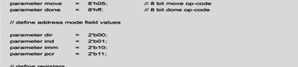
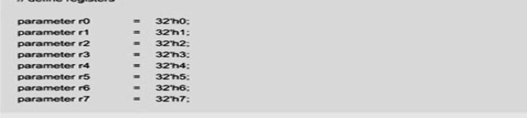
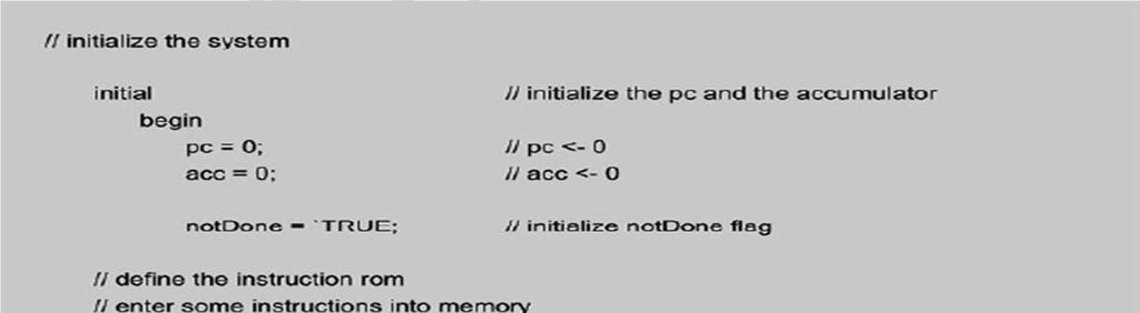
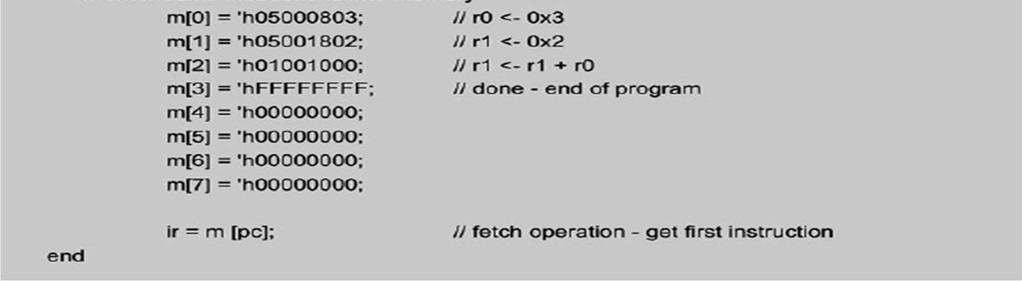
37 Next The address of the next instruction to be executed is dependent on the type of instruction to be executed and, potentially, on the state of the condition flags as modified by the recently completed instruction. At the end of the day, most reduce to algebraically adding a value to the PC. For short jumps, the displacement may be contained in one of the operand fields of the instruction; for longer jumps, the value may be contained in the memory location following the instruction. Thus, at the ISA level, the several versions of the next operation are written as ADD PC, offset; Algebraically modifying the PC is best accomplished by using one of the arithmetic functions in the ALU. The operation begins when the control logic places the desired offset into the ALU s temporary register. Next, the output of the PC is directed to the other ALU input. The ADD instruction is executed, and the result is entered into the PC. Placing a specific value into the PC can be done directly by the control logic since the target address is generally contained in the instruction. At the RTL level, the next step decomposes into the sequence of steps given in Figure Figure 2.48 The Next Sequence The Verilog program in Figure 2.49 implements a behavioural model of a portion of the datapath and control for the simple CPU presented at the start of this section. The number of registers has been reduced, only two instructions are implemented, and the address mode field supports four different modes. Nonetheless, the architecture implements a working system DEPT OF ECE, AGMRCET VARUR 37


38 DEPT OF ECE, AGMRCET VARUR 38


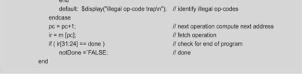
39 DEPT OF ECE, AGMRCET VARUR 39


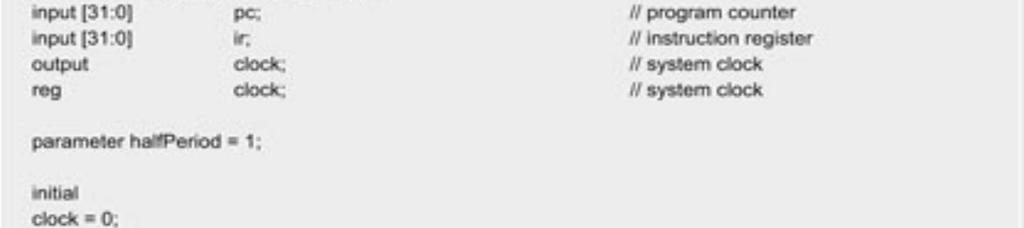
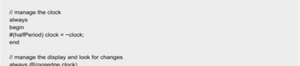
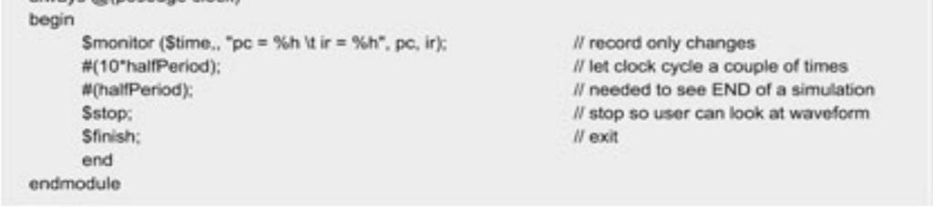
40 Figure 2.49 the simple CPU DEPT OF ECE, AGMRCET VARUR 40
41 The Hardware Side: Storage Elements and Finite-State Machines The hardware in the microprocessor is the digital circuits, the digital circuits are classified into two namely combinational and sequential logic circuits. In combinational logic circuits output depends on the primary state only. Examples of such circuits are adder, multiplexor, decoder and encoder In sequential logic circuit the output of the circuit depends upon the present input and past outputs. Examples of such circuits are latch, flipflop, counters and registers further sequential circuits are classified into synchronous sequential and asynchronous sequential circuit. To design such a complex systems we use finite state machine. Finite State Machine (FSM) used to describe the behaviour of digital circuits using finite no of states. The concepts of time and state In combinational circuit ignoring delay output is a function of input and no time constraints. In sequential circuits output depends on what time clock reaches the circuit?, what time we get output?, what time input reaches the circuit. Hence the time is the integrated behaviour of sequential circuits. State In general state represents to the condition things are in, what they are like at a particular time? In this context the state represents output of a circuit, there may be one or more states but each state must be represented uniquely. To represent the output we use several variables this set of variables is called state variables The state of the circuit will change depends on the input and state changes with respect to time is called behaviour of the system. State Diagram State diagram is a graphical representation of behaviour of the circuit, it us very useful in complex logic design. We show the transition between two states using a labelled directed line or arrow called an arc (or edge in graph theoretic language) as illustrated in Figure Because the line has a direction, the state diagram is referred to as a directed graph. The head or point of the arrow identifies the final state, and the tail or back of the arrow identifies the initial state. Special arcs, such as the one labelled initial, reflect an external, overriding asynchronous event, such as a reset, which places the system into a designated state, here state DEPT OF ECE, AGMRCET VARUR 41

42 a Because the graph can contain cycles, it is further qualified as a cyclic graph. The label on each identifies what caused the change and the output(s) of system, if appropriate. Figure 2.50 Transitions between States in a Digital Memory Device Example describe an evening s entertainment. Draw state diagram graphically to expresses the same behaviour that is described textually in Figure Finite State Machine A Theoretical Model Here we discuss different abstraction levels of Simple finite-state machines, the first view is as shown in Figure 2.53 have no inputs other than a clock and have only primitive outputs (we generally don t show the clock). Such machines are referred to as autonomous clocks. As we move to more complex designs, we will introduce inputs as well as more sophisticated outputs. A high-level block diagram for a finite-state machine begins with the diagram in Figure The outputs shown in the diagram may be the values of the state variables (as they will be in counting-type designs), combinations of the state variables, or combinations of the state variables and the inputs. Refining the level of detail the block diagram for the state machine appears as shown in Figure 2.55 DEPT OF ECE, AGMRCET VARUR 42


43 Figure 2.55 A High-Level Block Diagram for a Finite-State Machine We see first that the signals out of the finite-state machine decompose into two sets: state variables and outputs. Observe that the state variables are fed back as inputs to the system. The diagram illustrates the essence of the strength of the machine. It has the ability to recognize the state that it is in and then to react based on the values of the state variables and (potentially) to the inputs to the system. The decision as to which state to go to next is determined from the current input and the state that the machine is currently in. The present state of a finite-state machine inherently encodes the history of the path taken to get there. If we continue increasing the level of detail in the model, we now include the storage elements comprising the machine and the combinational logic that implements the output functionality and the input equations to the storage elements. The block diagram now becomes that in Figure The model has n inputs, m outputs, and p state variables. A memory device is associated with each state variable, and each state variable is associated with a memory device. At this point no particular type of memory device is specified DEPT OF ECE, AGMRCET VARUR 43
.")
44 We specify the set of variables Xi to represent the n inputs to the system; Zj to represent the m outputs from the system; and Yk to represent the p internal state variables. We define our finite-state machine as a quintuple (function of five). M = (I, O, S, λ,) I - Finite nonempty set or vector of inputs O - Finite nonempty set or vector of outputs S - Finite nonempty set or vector of states - Mapping I x S -> S λ 1 - Mapping I x S -> O - Mealy Machine λ 2 - Mapping S - O ->Moore Machine There are two types of Mealy and Moore machines. Mealy machine - λ 1 The output is a function of the present state and inputs Moore machine - λ 2 The output function of the present state only. Extensions to the basic diagram, such as we find in hardware/software co-design tools or the Unified Modelling Language (UML) state charts, support a rich set of system modelling capabilities. DEPT OF ECE, AGMRCET VARUR 44
Have difficulty identifying any products Not incorporating embedded processor FPGA or CPLD In one form or another
 Introduction Embedded systems Continue pervasive expansion into Vast variety of electronic systems and products Aircraft and automobiles games and medical equipment Have difficulty identifying any products
Objective now How are such control statements registers and other components Managed to ensure proper execution of each instruction
 Control and Control Components Introduction Software application similar to familiar nested Russian dolls As we ve observed earlier Application written in some high level programming language C, C++, C#,
Advanced Parallel Architecture Lesson 3. Annalisa Massini /2015
 Advanced Parallel Architecture Lesson 3 Annalisa Massini - 2014/2015 Von Neumann Architecture 2 Summary of the traditional computer architecture: Von Neumann architecture http://williamstallings.com/coa/coa7e.html
Module 5 - CPU Design
 Module 5 - CPU Design Lecture 1 - Introduction to CPU The operation or task that must perform by CPU is: Fetch Instruction: The CPU reads an instruction from memory. Interpret Instruction: The instruction
ASSEMBLY LANGUAGE MACHINE ORGANIZATION
 ASSEMBLY LANGUAGE MACHINE ORGANIZATION CHAPTER 3 1 Sub-topics The topic will cover: Microprocessor architecture CPU processing methods Pipelining Superscalar RISC Multiprocessing Instruction Cycle Instruction
Digital System Design Using Verilog. - Processing Unit Design
 Digital System Design Using Verilog - Processing Unit Design 1.1 CPU BASICS A typical CPU has three major components: (1) Register set, (2) Arithmetic logic unit (ALU), and (3) Control unit (CU) The register
Microcomputer Architecture and Programming
 IUST-EE (Chapter 1) Microcomputer Architecture and Programming 1 Outline Basic Blocks of Microcomputer Typical Microcomputer Architecture The Single-Chip Microprocessor Microprocessor vs. Microcontroller
Advanced Parallel Architecture Lesson 3. Annalisa Massini /2015
 Advanced Parallel Architecture Lesson 3 Annalisa Massini - Von Neumann Architecture 2 Two lessons Summary of the traditional computer architecture Von Neumann architecture http://williamstallings.com/coa/coa7e.html
CS 101, Mock Computer Architecture
 CS 101, Mock Computer Architecture Computer organization and architecture refers to the actual hardware used to construct the computer, and the way that the hardware operates both physically and logically
UNIT-II. Part-2: CENTRAL PROCESSING UNIT
 Page1 UNIT-II Part-2: CENTRAL PROCESSING UNIT Stack Organization Instruction Formats Addressing Modes Data Transfer And Manipulation Program Control Reduced Instruction Set Computer (RISC) Introduction:
EE 3170 Microcontroller Applications
 EE 3170 Microcontroller Applications Lecture 4 : Processors, Computers, and Controllers - 1.2 (reading assignment), 1.3-1.5 Based on slides for ECE3170 by Profs. Kieckhafer, Davis, Tan, and Cischke Outline
Introduction to Computers - Chapter 4
 Introduction to Computers - Chapter 4 Since the invention of the transistor and the first digital computer of the 1940s, computers have been increasing in complexity and performance; however, their overall
The CPU and Memory. How does a computer work? How does a computer interact with data? How are instructions performed? Recall schematic diagram:
 The CPU and Memory How does a computer work? How does a computer interact with data? How are instructions performed? Recall schematic diagram: 1 Registers A register is a permanent storage location within
DC57 COMPUTER ORGANIZATION JUNE 2013
 Q2 (a) How do various factors like Hardware design, Instruction set, Compiler related to the performance of a computer? The most important measure of a computer is how quickly it can execute programs.
Processing Unit CS206T
 Processing Unit CS206T Microprocessors The density of elements on processor chips continued to rise More and more elements were placed on each chip so that fewer and fewer chips were needed to construct
Chapter 2 Instruction Set Architecture
 Chapter 2 Instruction Set Architecture Course Outcome (CO) - CO2 Describe the architecture and organization of computer systems Program Outcome (PO) PO1 Apply knowledge of mathematics, science and engineering
The von Neumann Architecture. IT 3123 Hardware and Software Concepts. The Instruction Cycle. Registers. LMC Executes a Store.
 IT 3123 Hardware and Software Concepts February 11 and Memory II Copyright 2005 by Bob Brown The von Neumann Architecture 00 01 02 03 PC IR Control Unit Command Memory ALU 96 97 98 99 Notice: This session
8051 Overview and Instruction Set
 8051 Overview and Instruction Set Curtis A. Nelson Engr 355 1 Microprocessors vs. Microcontrollers Microprocessors are single-chip CPUs used in microcomputers Microcontrollers and microprocessors are different
Computer Architecture
 Computer Architecture Lecture 1: Digital logic circuits The digital computer is a digital system that performs various computational tasks. Digital computers use the binary number system, which has two
Latches. IT 3123 Hardware and Software Concepts. Registers. The Little Man has Registers. Data Registers. Program Counter
 IT 3123 Hardware and Software Concepts Notice: This session is being recorded. CPU and Memory June 11 Copyright 2005 by Bob Brown Latches Can store one bit of data Can be ganged together to store more
Segment 1A. Introduction to Microcomputer and Microprocessor
 Segment 1A Introduction to Microcomputer and Microprocessor 1.1 General Architecture of a Microcomputer System: The term microcomputer is generally synonymous with personal computer, or a computer that
Chapter 4. MARIE: An Introduction to a Simple Computer
 Chapter 4 MARIE: An Introduction to a Simple Computer Chapter 4 Objectives Learn the components common to every modern computer system. Be able to explain how each component contributes to program execution.
Introduction to Microcontrollers
 Introduction to Microcontrollers Embedded Controller Simply an embedded controller is a controller that is embedded in a greater system. One can define an embedded controller as a controller (or computer)
Basic Processing Unit: Some Fundamental Concepts, Execution of a. Complete Instruction, Multiple Bus Organization, Hard-wired Control,
 UNIT - 7 Basic Processing Unit: Some Fundamental Concepts, Execution of a Complete Instruction, Multiple Bus Organization, Hard-wired Control, Microprogrammed Control Page 178 UNIT - 7 BASIC PROCESSING
Universität Dortmund. ARM Architecture
 ARM Architecture The RISC Philosophy Original RISC design (e.g. MIPS) aims for high performance through o reduced number of instruction classes o large general-purpose register set o load-store architecture
COMPUTER ORGANIZATION & ARCHITECTURE
 COMPUTER ORGANIZATION & ARCHITECTURE Instructions Sets Architecture Lesson 5a 1 What are Instruction Sets The complete collection of instructions that are understood by a CPU Can be considered as a functional
CC312: Computer Organization
 CC312: Computer Organization Dr. Ahmed Abou EL-Farag Dr. Marwa El-Shenawy 1 Chapter 4 MARIE: An Introduction to a Simple Computer Chapter 4 Objectives Learn the components common to every modern computer
Chapter 3 : Control Unit
 3.1 Control Memory Chapter 3 Control Unit The function of the control unit in a digital computer is to initiate sequences of microoperations. When the control signals are generated by hardware using conventional
Chapter 3 - Top Level View of Computer Function
 Chapter 3 - Top Level View of Computer Function Luis Tarrataca luis.tarrataca@gmail.com CEFET-RJ L. Tarrataca Chapter 3 - Top Level View 1 / 127 Table of Contents I 1 Introduction 2 Computer Components
CS401 - Computer Architecture and Assembly Language Programming Glossary By
 CS401 - Computer Architecture and Assembly Language Programming Glossary By absolute address : A virtual (not physical) address within the process address space that is computed as an absolute number.
PESIT Bangalore South Campus
 INTERNAL ASSESSMENT TEST I Date: 30/08/2017 Max Marks: 40 Subject & Code: Computer Organization 15CS34 Semester: III (A & B) Name of the faculty: Mrs.Sharmila Banu.A Time: 8.30 am 10.00 am Answer any FIVE
Chapter 4. MARIE: An Introduction to a Simple Computer. Chapter 4 Objectives. 4.1 Introduction. 4.2 CPU Basics
 Chapter 4 Objectives Learn the components common to every modern computer system. Chapter 4 MARIE: An Introduction to a Simple Computer Be able to explain how each component contributes to program execution.
1. Fundamental Concepts
 1. Fundamental Concepts 1.1 What is a computer? A computer is a data processing machine which is operated automatically under the control of a list of instructions (called a program) stored in its main
CN310 Microprocessor Systems Design
 CN310 Microprocessor Systems Design Micro Architecture Nawin Somyat Department of Electrical and Computer Engineering Thammasat University 28 August 2018 Outline Course Contents 1 Introduction 2 Simple
STRUCTURE OF DESKTOP COMPUTERS
 Page no: 1 UNIT 1 STRUCTURE OF DESKTOP COMPUTERS The desktop computers are the computers which are usually found on a home or office desk. They consist of processing unit, storage unit, visual display
COMPUTER ARCHITECTURE AND ORGANIZATION Register Transfer and Micro-operations 1. Introduction A digital system is an interconnection of digital
 Register Transfer and Micro-operations 1. Introduction A digital system is an interconnection of digital hardware modules that accomplish a specific information-processing task. Digital systems vary in
ADVANCED COMPUTER ARCHITECTURE TWO MARKS WITH ANSWERS
 ADVANCED COMPUTER ARCHITECTURE TWO MARKS WITH ANSWERS 1.Define Computer Architecture Computer Architecture Is Defined As The Functional Operation Of The Individual H/W Unit In A Computer System And The
Chapter 7 Central Processor Unit (S08CPUV2)
") Chapter 7 Central Processor Unit (S08CPUV2) 7.1 Introduction This section provides summary information about the registers, addressing modes, and instruction set of the CPU of the HCS08 Family. For a more
Chapter 7 Central Processor Unit (S08CPUV2) 7.1 Introduction This section provides summary information about the registers, addressing modes, and instruction set of the CPU of the HCS08 Family. For a more
For your convenience Apress has placed some of the front matter material after the index. Please use the Bookmarks and Contents at a Glance links to
 For your convenience Apress has placed some of the front matter material after the index. Please use the Bookmarks and Contents at a Glance links to access them. Contents at a Glance About the Author...xi
ARM ARCHITECTURE. Contents at a glance:
 UNIT-III ARM ARCHITECTURE Contents at a glance: RISC Design Philosophy ARM Design Philosophy Registers Current Program Status Register(CPSR) Instruction Pipeline Interrupts and Vector Table Architecture
EC-801 Advanced Computer Architecture
 EC-801 Advanced Computer Architecture Lecture 5 Instruction Set Architecture I Dr Hashim Ali Fall 2018 Department of Computer Science and Engineering HITEC University Taxila!1 Instruction Set Architecture
Page 1. Structure of von Nuemann machine. Instruction Set - the type of Instructions
 Structure of von Nuemann machine Arithmetic and Logic Unit Input Output Equipment Main Memory Program Control Unit 1 1 Instruction Set - the type of Instructions Arithmetic + Logical (ADD, SUB, MULT, DIV,
Computer Architecture
 Computer Architecture Slide Sets WS 2013/2014 Prof. Dr. Uwe Brinkschulte M.Sc. Benjamin Betting Part 3 Fundamentals in Computer Architecture Computer Architecture Part 3 page 1 of 55 Prof. Dr. Uwe Brinkschulte,
Software and Hardware
 Software and Hardware Numbers At the most fundamental level, a computer manipulates electricity according to specific rules To make those rules produce something useful, we need to associate the electrical
Microcontroller Systems
 µcontroller systems 1 / 43 Microcontroller Systems Engineering Science 2nd year A2 Lectures Prof David Murray david.murray@eng.ox.ac.uk www.robots.ox.ac.uk/ dwm/courses/2co Michaelmas 2014 µcontroller
Microcontrollers. Microcontroller
 Microcontrollers Microcontroller A microprocessor on a single integrated circuit intended to operate as an embedded system. As well as a CPU, a microcontroller typically includes small amounts of RAM and
Von Neumann Architecture
 Von Neumann Architecture Assist lecturer Donya A. Khalid Lecture 2 2/29/27 Computer Organization Introduction In 945, just after the World War, Jon Von Neumann proposed to build a more flexible computer.
Chapter 17. Microprogrammed Control. Yonsei University
 Chapter 17 Microprogrammed Control Contents Basic Concepts Microinstruction Sequencing Microinstruction Execution TI 8800 Applications of Microprogramming 17-2 Introduction Basic Concepts An alternative
CPE 323 MSP430 INSTRUCTION SET ARCHITECTURE (ISA)
") CPE 323 MSP430 INSTRUCTION SET ARCHITECTURE (ISA) Aleksandar Milenković Email: milenka@uah.edu Web: http://www.ece.uah.edu/~milenka Objective Introduce MSP430 Instruction Set Architecture (Class of ISA,
CPE 323 MSP430 INSTRUCTION SET ARCHITECTURE (ISA) Aleksandar Milenković Email: milenka@uah.edu Web: http://www.ece.uah.edu/~milenka Objective Introduce MSP430 Instruction Set Architecture (Class of ISA,
COSC121: Computer Systems: Review
 COSC121: Computer Systems: Review Jeremy Bolton, PhD Assistant Teaching Professor Constructed using materials: - Patt and Patel Introduction to Computing Systems (2nd) - Patterson and Hennessy Computer
 Chapter 1 Microprocessor architecture ECE 3120 Dr. Mohamed Mahmoud http://iweb.tntech.edu/mmahmoud/ mmahmoud@tntech.edu Outline 1.1 Computer hardware organization 1.1.1 Number System 1.1.2 Computer hardware
Computer Science 324 Computer Architecture Mount Holyoke College Fall Topic Notes: Data Paths and Microprogramming
 Computer Science 324 Computer Architecture Mount Holyoke College Fall 2007 Topic Notes: Data Paths and Microprogramming We have spent time looking at the MIPS instruction set architecture and building
Block diagram view. Datapath = functional units + registers
 Computer design an application of digital logic design procedures Computer = processing unit + memory system Processing unit = control + datapath Control = finite state machine inputs = machine instruction,
For Example: P: LOAD 5 R0. The command given here is used to load a data 5 to the register R0.
 Register Transfer Language Computers are the electronic devices which have several sets of digital hardware which are inter connected to exchange data. Digital hardware comprises of VLSI Chips which are
Blog -
 . Instruction Codes Every different processor type has its own design (different registers, buses, microoperations, machine instructions, etc) Modern processor is a very complex device It contains Many
Computer Systems. Binary Representation. Binary Representation. Logical Computation: Boolean Algebra
 Binary Representation Computer Systems Information is represented as a sequence of binary digits: Bits What the actual bits represent depends on the context: Seminar 3 Numerical value (integer, floating
Wednesday, September 13, Chapter 4
 Wednesday, September 13, 2017 Topics for today Introduction to Computer Systems Static overview Operation Cycle Introduction to Pep/9 Features of the system Operational cycle Program trace Categories of
EC 413 Computer Organization
 EC 413 Computer Organization Review I Prof. Michel A. Kinsy Computing: The Art of Abstraction Application Algorithm Programming Language Operating System/Virtual Machine Instruction Set Architecture (ISA)
5.7. Microprogramming: Simplifying Control Design 5.7
 5.7 Microprogramming: Simplifying Control Design 5.7 For the of our simple MIPS subset, a graphical representation of the finite state machine, as in Figure 5.40 on page 345, is certainly adequate. We
Rui Wang, Assistant professor Dept. of Information and Communication Tongji University.
 Instructions: ti Language of the Computer Rui Wang, Assistant professor Dept. of Information and Communication Tongji University it Email: ruiwang@tongji.edu.cn Computer Hierarchy Levels Language understood
COMPUTER ORGANIZATION AND ARCHITECTURE
 Page 1 1. Which register store the address of next instruction to be executed? A) PC B) AC C) SP D) NONE 2. How many bits are required to address the 128 words of memory? A) 7 B) 8 C) 9 D) NONE 3. is the
Chapter 12. CPU Structure and Function. Yonsei University
 Chapter 12 CPU Structure and Function Contents Processor organization Register organization Instruction cycle Instruction pipelining The Pentium processor The PowerPC processor 12-2 CPU Structures Processor
Blog - https://anilkumarprathipati.wordpress.com/
 Control Memory 1. Introduction The function of the control unit in a digital computer is to initiate sequences of microoperations. When the control signals are generated by hardware using conventional
CS 2461: Computer Architecture I
 Computer Architecture is... CS 2461: Computer Architecture I Instructor: Prof. Bhagi Narahari Dept. of Computer Science Course URL: www.seas.gwu.edu/~bhagiweb/cs2461/ Instruction Set Architecture Organization
Top-Level View of Computer Organization
 Top-Level View of Computer Organization Bởi: Hoang Lan Nguyen Computer Component Contemporary computer designs are based on concepts developed by John von Neumann at the Institute for Advanced Studies
MARIE: An Introduction to a Simple Computer
 MARIE: An Introduction to a Simple Computer Outline Learn the components common to every modern computer system. Be able to explain how each component contributes to program execution. Understand a simple
Chapter 4. Chapter 4 Objectives. MARIE: An Introduction to a Simple Computer
 Chapter 4 MARIE: An Introduction to a Simple Computer Chapter 4 Objectives Learn the components common to every modern computer system. Be able to explain how each component contributes to program execution.
COS 140: Foundations of Computer Science
 COS 140: Foundations of Computer Science CPU Organization and Assembly Language Fall 2018 CPU 3 Components of the CPU..................................................... 4 Registers................................................................
What Are The Main Differences Between Program Counter Pc And Instruction Register Ir
 What Are The Main Differences Between Program Counter Pc And Instruction Register Ir and register-based instructions - Anatomy on a CPU - Program Counter (PC): holds memory address of next instruction
The MARIE Architecture
 The MARIE Machine Architecture that is Really Intuitive and Easy. We now define the ISA (Instruction Set Architecture) of the MARIE. This forms the functional specifications for the CPU. Basic specifications
Laboratory Exercise 3 Comparative Analysis of Hardware and Emulation Forms of Signed 32-Bit Multiplication
 Laboratory Exercise 3 Comparative Analysis of Hardware and Emulation Forms of Signed 32-Bit Multiplication Introduction All processors offer some form of instructions to add, subtract, and manipulate data.
Multi Cycle Implementation Scheme for 8 bit Microprocessor by VHDL
 Multi Cycle Implementation Scheme for 8 bit Microprocessor by VHDL Sharmin Abdullah, Nusrat Sharmin, Nafisha Alam Department of Electrical & Electronic Engineering Ahsanullah University of Science & Technology
Register Are Two Names For The Same Place
 The Program Counter And The Instruction Register Are Two Names For The Same Place Hi I am wondering where the program counter goes when the program The interrupt will take place after the current iteration
Computer Organization and Technology Processor and System Structures
 Computer Organization and Technology Processor and System Structures Assoc. Prof. Dr. Wattanapong Kurdthongmee Division of Computer Engineering, School of Engineering and Resources, Walailak University
In examining performance Interested in several things Exact times if computable Bounded times if exact not computable Can be measured
 System Performance Analysis Introduction Performance Means many things to many people Important in any design Critical in real time systems 1 ns can mean the difference between system Doing job expected
MICROPROCESSOR AND MICROCONTROLLER BASED SYSTEMS
 MICROPROCESSOR AND MICROCONTROLLER BASED SYSTEMS UNIT I INTRODUCTION TO 8085 8085 Microprocessor - Architecture and its operation, Concept of instruction execution and timing diagrams, fundamentals of
Overview. EE 4504 Computer Organization. Much of the computer s architecture / organization is hidden from a HLL programmer
 Overview EE 4504 Computer Organization Section 7 The Instruction Set Much of the computer s architecture / organization is hidden from a HLL programmer In the abstract sense, the programmer should not
CHAPTER ASSEMBLY LANGUAGE PROGRAMMING
 CHAPTER 2 8051 ASSEMBLY LANGUAGE PROGRAMMING Registers Register are used to store information temporarily: A byte of data to be processed An address pointing to the data to be fetched The vast majority
CS6303 Computer Architecture Regulation 2013 BE-Computer Science and Engineering III semester 2 MARKS
 CS6303 Computer Architecture Regulation 2013 BE-Computer Science and Engineering III semester 2 MARKS UNIT-I OVERVIEW & INSTRUCTIONS 1. What are the eight great ideas in computer architecture? The eight
DSP Platforms Lab (AD-SHARC) Session 05
 Session 05") University of Miami - Frost School of Music DSP Platforms Lab (AD-SHARC) Session 05 Description This session will be dedicated to give an introduction to the hardware architecture and assembly programming
University of Miami - Frost School of Music DSP Platforms Lab (AD-SHARC) Session 05 Description This session will be dedicated to give an introduction to the hardware architecture and assembly programming
Understanding the basic building blocks of a microcontroller device in general. Knows the terminologies like embedded and external memory devices,
 Understanding the basic building blocks of a microcontroller device in general. Knows the terminologies like embedded and external memory devices, CISC and RISC processors etc. Knows the architecture and
Computer Organization and Levels of Abstraction
 Computer Organization and Levels of Abstraction Announcements Today: PS 7 Lab 8: Sound Lab tonight bring machines and headphones! PA 7 Tomorrow: Lab 9 Friday: PS8 Today (Short) Floating point review Boolean
Note that none of the above MAY be a VALID ANSWER.
 ECE 270 Learning Outcome 4-1 - Practice Exam / Solution OUTCOME #4: An ability to design and implement computer logic circuits. Multiple Choice select the single most appropriate response for each question.
ADDRESS GENERATION UNIT (AGU)
") nc. SECTION 4 ADDRESS GENERATION UNIT (AGU) MOTOROLA ADDRESS GENERATION UNIT (AGU) 4-1 nc. SECTION CONTENTS 4.1 INTRODUCTION........................................ 4-3 4.2 ADDRESS REGISTER FILE (Rn)............................
nc. SECTION 4 ADDRESS GENERATION UNIT (AGU) MOTOROLA ADDRESS GENERATION UNIT (AGU) 4-1 nc. SECTION CONTENTS 4.1 INTRODUCTION........................................ 4-3 4.2 ADDRESS REGISTER FILE (Rn)............................
COMP2121: Microprocessors and Interfacing. Instruction Set Architecture (ISA)
") COMP2121: Microprocessors and Interfacing Instruction Set Architecture (ISA) http://www.cse.unsw.edu.au/~cs2121 Lecturer: Hui Wu Session 2, 2017 1 Contents Memory models Registers Data types Instructions
COMP2121: Microprocessors and Interfacing Instruction Set Architecture (ISA) http://www.cse.unsw.edu.au/~cs2121 Lecturer: Hui Wu Session 2, 2017 1 Contents Memory models Registers Data types Instructions
CPU. Fall 2003 CSE 207 Digital Design Project #4 R0 R1 R2 R3 R4 R5 R6 R7 PC STATUS IR. Control Logic RAM MAR MDR. Internal Processor Bus
 http://www.engr.uconn.edu/~barry/cse207/fa03/project4.pdf Page 1 of 16 Fall 2003 CSE 207 Digital Design Project #4 Background Microprocessors are increasingly common in every day devices. Desktop computers
Typical Processor Execution Cycle
 Typical Processor Execution Cycle Instruction Fetch Obtain instruction from program storage Instruction Decode Determine required actions and instruction size Operand Fetch Locate and obtain operand data
COMP3221: Microprocessors and. and Embedded Systems. Instruction Set Architecture (ISA) What makes an ISA? #1: Memory Models. What makes an ISA?
 What makes an ISA? #1: Memory Models. What makes an ISA?") COMP3221: Microprocessors and Embedded Systems Lecture 2: Instruction Set Architecture (ISA) http://www.cse.unsw.edu.au/~cs3221 Lecturer: Hui Wu Session 2, 2005 Instruction Set Architecture (ISA) ISA is
COMP3221: Microprocessors and Embedded Systems Lecture 2: Instruction Set Architecture (ISA) http://www.cse.unsw.edu.au/~cs3221 Lecturer: Hui Wu Session 2, 2005 Instruction Set Architecture (ISA) ISA is
Computer Organization CS 206 T Lec# 2: Instruction Sets
 Computer Organization CS 206 T Lec# 2: Instruction Sets Topics What is an instruction set Elements of instruction Instruction Format Instruction types Types of operations Types of operand Addressing mode
Arab Open University. Computer Organization and Architecture - T103
 Arab Open University Computer Organization and Architecture - T103 Reference Book: Linda Null, Julia Lobur, The essentials of Computer Organization and Architecture, Jones & Bartlett, Third Edition, 2012.
The LC3's micro-coded controller ("useq") is nothing more than a finite-state machine (FSM). It has these inputs:
 is nothing more than a finite-state machine (FSM). It has these inputs:") midterm exam COSC-120, Computer Hardware Fundamentals, fall 2012 Computer Science Department Georgetown University NAME Open books, open notes (laptops included). Show and explain all your work. Answers
midterm exam COSC-120, Computer Hardware Fundamentals, fall 2012 Computer Science Department Georgetown University NAME Open books, open notes (laptops included). Show and explain all your work. Answers
Wednesday, February 4, Chapter 4
 Wednesday, February 4, 2015 Topics for today Introduction to Computer Systems Static overview Operation Cycle Introduction to Pep/8 Features of the system Operational cycle Program trace Categories of
Chapter 3 Machine Instructions & Programs. Jin-Fu Li Department of Electrical Engineering National Central University Jungli, Taiwan
 Chapter 3 Machine Instructions & Programs Jin-Fu Li Department of Electrical Engineering National Central University Jungli, Taiwan Outline Numbers, Arithmetic Operations, and Characters Memory Locations
V8-uRISC 8-bit RISC Microprocessor AllianceCORE Facts Core Specifics VAutomation, Inc. Supported Devices/Resources Remaining I/O CLBs
 V8-uRISC 8-bit RISC Microprocessor February 8, 1998 Product Specification VAutomation, Inc. 20 Trafalgar Square Nashua, NH 03063 Phone: +1 603-882-2282 Fax: +1 603-882-1587 E-mail: sales@vautomation.com
von Neumann Architecture Basic Computer System Early Computers Microprocessor Reading Assignment An Introduction to Computer Architecture
 Reading Assignment EEL 4744C: Microprocessor Applications Lecture 1 Part 1 An Introduction to Computer Architecture Microcontrollers and Microcomputers: Chapter 1, Appendix A, Chapter 2 Software and Hardware
Basic Computer System. von Neumann Architecture. Reading Assignment. An Introduction to Computer Architecture. EEL 4744C: Microprocessor Applications
 Reading Assignment EEL 4744C: Microprocessor Applications Lecture 1 Part 1 An Introduction to Computer Architecture Microcontrollers and Microcomputers: Chapter 1, Appendix A, Chapter 2 Software and Hardware
SECTION 5 PROGRAM CONTROL UNIT
 SECTION 5 PROGRAM CONTROL UNIT MOTOROLA PROGRAM CONTROL UNIT 5-1 SECTION CONTENTS SECTION 5.1 PROGRAM CONTROL UNIT... 3 SECTION 5.2 OVERVIEW... 3 SECTION 5.3 PROGRAM CONTROL UNIT (PCU) ARCHITECTURE...
Question Bank Microprocessor and Microcontroller
 QUESTION BANK - 2 PART A 1. What is cycle stealing? (K1-CO3) During any given bus cycle, one of the system components connected to the system bus is given control of the bus. This component is said to
PROBLEMS. 7.1 Why is the Wait-for-Memory-Function-Completed step needed when reading from or writing to the main memory?
 446 CHAPTER 7 BASIC PROCESSING UNIT (Corrisponde al cap. 10 - Struttura del processore) PROBLEMS 7.1 Why is the Wait-for-Memory-Function-Completed step needed when reading from or writing to the main memory?
CPU ARCHITECTURE. QUESTION 1 Explain how the width of the data bus and system clock speed affect the performance of a computer system.
 CPU ARCHITECTURE QUESTION 1 Explain how the width of the data bus and system clock speed affect the performance of a computer system. ANSWER 1 Data Bus Width the width of the data bus determines the number